 C. F. Bedoya1
 S. Cuadrado1J. Cuchillo1
 D. Eliseev2
 N. Esper2D. Francia1
 A. Navarro1R. Paz1C. Presser2
 I. Redondo1*D. D. Redondo1J. Sastre1
- 1Department of Basic Research, Centro de Investigaciones Medioambientales y Tecnológicas, Madrid, Spain
- 2III. Physics Institute A, RWTH Aachen University, Aachen, Germany
A new readout board for the digitization of the CMS (Compact Muon Solenoid) Muon Drift Tube (DT) chambers has been designed in order to cope with the increase of occupancy and trigger rates expected during operation under the foreseen luminosity in the HL-LHC (High Luminosity Large Hadron Collider). The board OBDT-theta (On-detector Board for Drift Tubes) can perform the time digitization and readout of the DT chamber signals measuring the z-coordinate (along the beam axis) of CMS. A total of 228 channels can be digitized with a time bin of 0.78 ns and full streaming of all the DT chamber signals can be made through optical links into the CMS counting room. There, the full detector information can be available to perform the trigger and event building logic. The different functionality of the OBDT-theta board has been verified and the overall architecture has been validated through specific tests. The OBDT-theta architecture and main functionality will be presented in this contribution, showing the suitability of the design for the expected functionality during the HL-LHC.
1 Introduction
The Large Hadron Collider (LHC) has been instrumental in advancing our understanding of particle physics, most notably through the discovery of the Higgs boson and precise tests of the Standard Model, while also pushing the boundaries in the search for new physics.
In order to enable the study of rare processes and new physics with even greater precision, the LHC is undergoing a major upgrade: the High-Luminosity LHC (HL-LHC) (Apollinari et al., 2017). This upgrade, set to be completed in the coming years, aims to increase the collider integrated luminosity by a factor of 10 compared to its current capacity. Luminosity, which relates to the number of collisions produced within the accelerator, is critical for improving the precision of experimental measurements and enhancing the discovery potential for rare processes. The HL-LHC will allow refining precision measurements, explore rare phenomena, investigate the Higgs boson in detail and search for new physics.
The HL-LHC upgrade will have a profound impact on the detectors used in the major experiments such as CMS (Compact Muon Solenoid), which must undergo significant upgrades to handle the higher radiation levels, increased data rates, and enhanced event complexity.
The muon detectors play a central role in CMS (CMS Collaboration, 1997), as muons can be identified and measured individually and accurately, and they stand out from the large hadronic background typical of hadron colliders. In the central region of CMS, the Drift Tube (DT) detector is crucial to perform trigger and muon identification and reconstruction. Ensuring that these muon detectors maintain their performance throughout HL-LHC is critical to guarantee an excellent physics performance of the CMS detector.
The Drift Tube detector is a key component of the muon detection system that performs muon identification, triggering and reconstruction and is located in the barrel region of the CMS detector covering the pseudo-rapidity range −1.2 < η < 1.2. The basic detector element is a rectangular drift cell with a transversal size of 4.2 cm × 1.3 cm filled with a 85%/15% Ar/CO2 gas mixture. The cell is delimited by aluminum (Al) beams on the sides, where cathodes are located, and by Al plates on the top and bottom, which also separate the detection layers. Attached to these plates through a Mylar insulation there are Al strip electrodes that shape the electric field to achieve constant drift velocity along the cell. Inside each of these cells, a 50 µm diameter gold-plated steel wire acts as the anode.
When a charged particle, such as a muon, passes through the tube, it ionizes the gas. The resulting free electrons drift toward the central wire at a constant velocity, where they create an electric signal that is used to determine the particle position within the tube through the measurement of the time of arrival of this signal. The DT detectors work by exploiting the time it takes for ionized electrons to drift toward the central wire, which provides spatial information about the particle path. By combining the signals from multiple tubes, a precise 3D track of the muon can be reconstructed.
DT cells form layers, and stacks of four layers, staggered by half a cell, are assembled to form a SuperLayer (SL). A DT chamber is made of a block of two SLs measuring the ϕ coordinate plus one SL measuring the z or θ coordinate, coordinates referring to the CMS polar reference system1. A schematic view of the CMS DT chamber is shown in Figure 1. There are a total of 250 DT chambers in the CMS detector, distributed in 5 wheels. Each wheel is subdivided in twelve 30° sectors and each sector contains 4 DT chambers at increasing distances of the CMS interaction point.
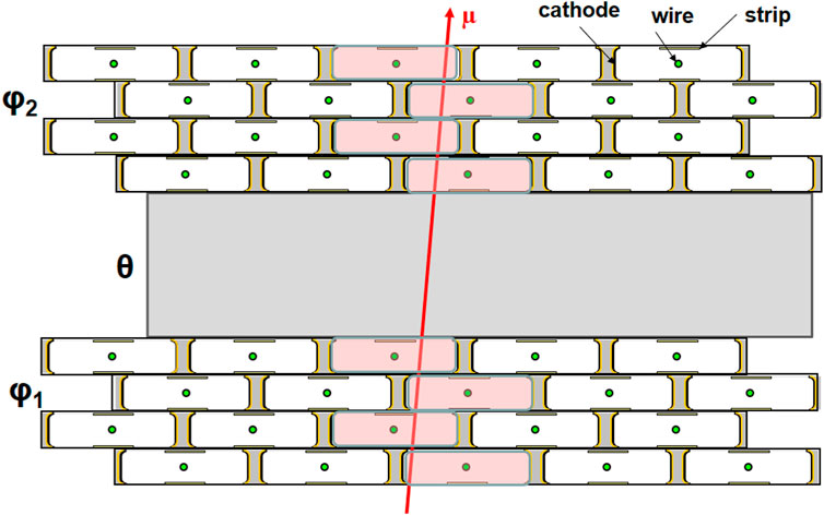
Figure 1. Schematic layout of a CMS Drift Tube chamber. The innermost and outermost SuperLayers measure the r-φ coordinate in the bending plane of the CMS magnet; the SL2 SuperLayer measures the z coordinate, along the direction parallel to the beam (perpendicular to the plane of the Figure). Each SL is made of four layers of drift cells, and each drift cell is made of a wire enclosed in two cathodes and two strips.
Several studies throughout the years (CMS Collaboration, 2017) have established that the DT chambers are expected to survive efficiently the integrated charge expected throughout the HL-LHC, including the Front End Boards (FEBs) inside the chamber that perform the signal pre-amplification and shaping. However, the electronics system attached to the DT chambers will need to be replaced. On one hand, there is concern about the obsolescence of the legacy electronics built in 2003, which is a complex system that does not seem to be radiation tolerant enough for the full duration of the HL-LHC phase.
The DT on-detector electronics is embedded in an aluminum structure, called Minicrate, which is attached to the structure of the DT chamber and remains enclosed inside the CMS wheels. At present this system is made of up to 17 boards per Minicrate of several types, heavily interconnected and compacted in a very tight structure with high power consumption, posing concerns about its longevity.
On the other hand, the expected Level 1 Accept (L1A) trigger rates at which CMS is expected to operate to cope with the higher luminosity will increase from the current 100 kHz up to 750 kHz (CMS Collaboration, 2020). Studies performed with the present readout system show that it will not be capable of sustaining this rate, becoming highly inefficient beyond 300 kHz.
Accordingly, a new system that substitutes the existing Minicrates with radiation-tolerant electronics that can read out the DT chambers at the expected rates without inefficiencies is required. The present technology allows for the implementation of a full streaming system, where all the DT generated data can be transmitted outside of the radiation environment becoming independent of the L1A rate.
A new board, called OBDT (On detector Board for Drift Tubes), is being developed to be used for replacing the on-detector electronics of the CMS Drift Tubes. Its main functionality is performing the time digitization and further readout of LVDS signals and transmitting them without inefficiency outside the experimental cavern.
To read out 172,200 channels from the DT chambers, 830 OBDTs will be needed. There will be two types of OBDT boards, 180 of which will digitize the signals from the wires that measure the θ coordinate. This type of board is called OBDT-theta and is the subject of this contribution: the OBDT-theta. The two boards have slightly different requirements, the most critical one being the necessity to maintain the legacy cables and connectors in the θ view, due to the impossibility to extract all the DT chambers outside of the CMS steel wheels.
2 The OBDT-theta board
The OBDT-theta board has been designed to perform the time digitization of a total of 228 channels with a time resolution of 0.78 ns. To achieve a high integration, the board has been built using a Microchip Polarfire FPGA MPF300T-1FCG1152E, responsible for the time digitization of the incoming pseudo-digital signals. The Polarfire FPGA is built on state-of-the-art 28 nm non-volatile process technology and uses SONOS non-volatile (NV) technology. Several radiation campaigns (Redondo et al., 2024) have proven the capability of the boards of safely standing the expected levels of radiation in the region of the CMS DT chambers, which should be below 10 Gy after 10 years of operation of HL-LHC.
The 228 channels are input to the board through eight 68-pin SCSI connectors, which are compatible with the current CMS DT cables in the θ view. The input signals are compatible with LVDS square pulses with at most 150 ns width. The time measurement is performed on the rising edge of each pulse.
The OBDT-theta board needs to be synchronized with the LHC 40.078 MHz clock and thus, it uses the lpGBT (Guettouche et al., 2022) ASIC from CERN that provides the clock and fast timing signals reception as well as a communication link for configuration and monitoring. The lpGBT is also connected to a GigaBit Transceiver Slow Control Adapter (GBT-SCA) (Caratelli et al., 2015) ASIC from CERN, which allows you to implement several features such as: analog to digital conversion of multiple voltage levels for voltages, current and temperature monitoring, generation of voltage levels required by the DT chambers and remote reconfiguration of the Polarfire FPGA through a Serial Peripheral Interface (SPI). To have a redundant system, a secondary slow control bidirectional link is built from the Polarfire FPGA directly.
The FPGA, after performing the time digitization, needs to funnel the information into one or several high speed links for transmission to the backend. Up to 6 high-speed links, which use the lpGBT protocol at 10.24 Gpbs, are output from the FPGA and sent through optical fibers using two VTRX+ (CERN, 2025) optical transceivers from CERN.
Finally, the OBDT-theta will have the possibility to interface to external components through several I2C interfaces such as the FEBs inside the DT chambers. Additionally, an external board, called Testpulse-theta, will be used for generating calibration signals to synchronize the DT system.
The overall architecture of the OBDT-theta board is shown in Figure 2 and an image of the OBDT-theta board is shown in Figure 3.
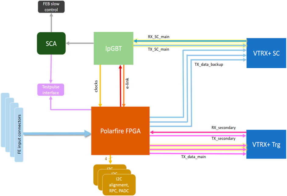
Figure 2. Architecture of the OBDT-theta board with its main components.
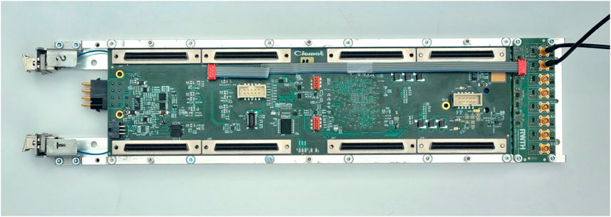
Figure 3. Image of the final OBDT-theta board assembled in its mechanical structure together with the OBDT-theta testpulse board.
2.1 Time digitization
As mentioned, the time digitization of the input signals will be performed inside the FPGA, and both a coarse and a fine time measurement will be performed. The coarse measurement is performed with a 12-bit counter driven with a 40 MHz clock, i.e., the counting unit is 25 ns. Its dynamic range will be reduced from 4096 to 3564, in order to stay synchronized with the LHC orbit.
The fine measurement is performed using a deserialization method inside the FPGA. A deserializer module is implemented on each of the 228 differential input channels and is operated at 640 MHz in DDR (Double Data Rate) mode, that is effectively 1.2 GHz, which provides a time bin of 0.78 ns. Therefore, up to 5 bits are used to code the fine time measurement.
Both the coarse and fine time measurements of each signal are combined with the information of the channel number to provide a 25-bit digital word. All the time measurements are referred to a periodic signal called BC0 (Bunch Crossing 0), which can be received externally or generated internally. For operation under LHC, this signal is expected to arrive synchronously through the TCDS (Timing and Control Detector System) (Hegeman et al., 2015) and mark the start of a new LHC orbit, which is repeated after 3564 clock cycles of 25 ns (i.e., bunch crossings). The TDC architecture implemented in the firmware is shown in Figure 4 and a timing diagram is shown in Figure 5.
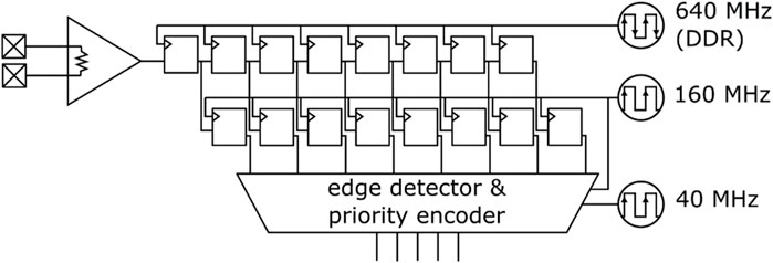
Figure 4. The TDC architecture is shown, with the input differential signal, the deserializer flip-flops and the firmware blocks of edge detection and encoding. The different clocks used in the different regions are indicated.
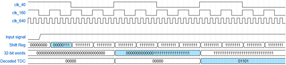
Figure 5. Timing diagram of the time digitization implemented through the deserialization method. The different clocks used are represented, as well as the input signal received at the OBDT-theta, the shift registers obtained from the deserialization stage and the final decoded time word of the fine time measurement.
In the foreseen operation mode, each time measurement is expected to be made of the time at which the collision took place (certain number of 25 ns clock cycles after the BC0), the time of flight of the muon to the actual DT cell and the drift time of the electron to the anode. This last contribution is the one that is expected to be proportional to the position of the muon inside the cell due to a constant drift velocity which is set to be ∼54.4 μm/ns by carefully controlling the gas mixture, which needs to remain stable. This drift velocity provides a good position resolution, but the value itself is not as critical as its stability. Additional contributions to the time measurement are expected from the delay introduced by the cables or the anode wire itself. These contributions need to be corrected during the DT system calibration procedure. The bunch crossing at which the muon was generated should be marked by the L1A generated by the CMS Trigger system.
2.2 Power distribution
The OBDT-theta requires two voltage rails: 5 V, used to power external interfaces and the Testpulse-theta board and, 3.3 V, used for all the digital parts. For basic operation of the OBDT-theta, only 3 V is required.
The OBDT-theta power distribution relies on low voltage drop linear regulators of the type MIC69502WR, which can provide up to 5 A in case it is needed by the final design of the FPGA. Because of the low voltage acceptance of this regulator, the MIC29302AWD linear regulator is used instead for the 5 V rail. These regulators have been repeatedly tested under radiation by our group, providing good results in terms of small variations of the regulated voltage and small increases of the dark current.
Up to 5 different voltages are generated by these linear regulators: 1.05 V and 1.8 V for powering the FPGA core, 1.5 V for the SCA ASIC, 1.2 V for the lpGBT and 2.5 V for the input/output banks of the FPGA and the optical transceivers. The transceivers of the FPGA are also powered through an independent voltage regulator.
The total power consumption of the board is highly dependent on the FPGA implementation but the estimations performed with the present firmware offer values of 2.7 A in the 3 V rail and 0.1 A on the 5 V rail. The total power consumption is expected to be ∼9 W.
The linear regulators are controlled by a signal that is generated by the safety system of the OBDT. Its timing can also be controlled if required, although this was not needed to safely power on the board and the FPGA. Adequate capacitance was selected to ensure a smooth voltage ramp up in the board and match the expected long power cables. The use of inductances has been minimized to some air core ones to guarantee safe operation under magnetic fields.
2.3 Safety system
The OBDT-theta board is expected to be operational in an inaccessible location, enclosed into the CMS wheels, where access can only happen, if any, every several years. Accordingly, not only the power consumption needs to be minimized but also, a safety system is beneficial to protect the board against unexpected failures. Major protections have been put in place for the following events: overvoltage, overcurrent and temperature.
Temperature is measured on the board through up to six PT1000 platinum sensors. Two of them, one located near the warmer place in the linear regulators and another one close to the FPGA and transceivers, are able to power down the board. An overtemperature alarm is provided through operational amplifiers that compare voltages to reference ones and activate a digital logic chain that acts on the enable signal of the linear regulators.
Similarly, 5 V overvoltage and overcurrent protection is implemented through the MAX4374TEUB + device which allows current sensing and comparison with a reference voltage, activating a logic circuit that powers down the regulators.
Overvoltage protection for the 3 V rail is built somehow differently because the input to the linear regulators need to be protected over 6 V. Accordingly, the output of the comparators acts directly on a MOSFET device that totally cuts the 3 V input voltage to the board, protecting the regulators. A reverse voltage protection through a diode has also been put in place.
As expected, the safety part of the OBDT board cannot be powered down by itself, remaining active when the MOSFETs or regulators are powered down. However, it is in charge of activating an ALARM signal that can be transmitted to an external system as a flag. It also contains an input signal that is received through an optocoupler and disables the linear regulators if desired. The power consumption of the safety system is small (∼20 mA) and considered minimally dangerous.
2.4 Slow control and timing distribution
The OBDT-theta is expected to be configured and monitored through a Slow Control Link, the lpGBT, from which several devices in the board profit. The SCA and the Polarfire FPGA contain different configuration registers that allow you to modify the OBDT-theta behavior and/or its performance.
In addition, the OBDT-theta is expected to receive a clock synchronous to the LHC and at least a signal marking the start of the LHC orbit (called Bunch Crossing 0, BC0). Other fast commands, that can be used to activate the calibration system, need to be distributed too.
The CERN Versatile Link project is an initiative aimed at developing a robust, radiation-tolerant, high-speed optical link system for data transmission in particle detectors, particularly in the upgraded systems of the HL-LHC. This project focuses on providing reliable, bidirectional communication between the detector electronics and the remote data acquisition systems. It supports data rates up to 10.24 Gbps and is designed to withstand the intense radiation and magnetic fields present in the detector areas, ensuring that high-quality data communication is maintained during operations. The Versatile Link provides a mechanism for distributing the global clock signal from the centralized timing system to the front-end electronics. The clock is embedded within the data stream, ensuring that timing information is delivered alongside the detector data, allowing for accurate synchronization and reducing jitter.
The lpGBT ASIC has been designed to interface through the VTRX+, which is a module that includes custom radiation-tolerant optical transceivers. The VTRX+ includes four transmission links at up to 10.24 Gbps and one receiver link at 2.56 Gbps. Both the 2.56 Gbps and one transmission link are needed for configuration and monitoring of the OBDT-theta from the backend and for receiving the clock and the fast signals.
The lpGBT is in charge of recovering the operation clock and distributing it to the Polarfire FPGA. In addition, it implements a so-called E-link protocol for communication with external sources, in our case, the SCA ASIC and the Polarfire FPGA. The E-link is an electrical interface suitable for transmission of data through an electrical medium, within a distance of a few meters, at data rates up to 320 Mbps.
Another VTRX+ board is assembled in the OBDT and connects all of its electrical links directly to the Polarfire. This allows you to implement a secondary timing and slow control link, directly inside the Polarfire firmware, which is also capable of recovering the LHC clock. A dedicated quarz oscillator is also present in the board for clock reference in the transceivers.
The data transmission of the time measurements happens from the Polarfire directly, which is connected to up to 5 high speed links at 10.24 Gbps distributed among the two VTRX+ for data readout (one additional high speed link is used for slow control). The transmission protocol implemented in the Polarfire follows the firmware of the lpGBT protocol. This protocol provides two decoding schemes (FEC5 or FEC12) based on Reed-Solomon techniques to configure the encoding robustness. Using the more robust FEC12, the total user data available bandwidth per link is ∼8.1 Gbps, thus the total OBDT-theta throughput can reach ∼32.3 Gbps of readout bandwidth.
The GBT-SCA ASIC, or SCA, is used in the OBDT-theta board to provide some extra monitoring and configuration functionality. The main functionality that we use is:
- ADC (Analog to Digital Converter): We use 29 of the available inputs to perform the digitization of voltages throughout the board. This allows to monitor the voltages, currents and temperatures of the OBDT-theta, the received signal strength (RSSI) from the VTRX+ optical receivers, the humidity in the cavern through a dedicated sensor and the output of a water leak sensor in the OBDT-theta. In Figure 6 an image of this water leak sensor with and without a water drop can be seen. In addition, the measured values in the ADC of the output of the water leak sensor electronics can be seen for both dry and wet conditions.
- DAC (Digital to Analog Converter): One output is used to generate a voltage level that is sent to the Testpulse-theta board to establish the amplitude of the generated calibration signal.
- JTAG and SPI interface to the Polarfire FPGA. These interfaces allow remote reconfiguration of the Polarfire FPGA firmware in its internal Flash memory, in case of need.
- Additional digital signals to act on the OBDT-theta functionality. Examples are signals to reinitialize the Polarfire FPGA, to enable the SPI or JTAG access, to reset the lpGBT or to disable the humidity sensor, which is expected to operate only outside the LHC operation.
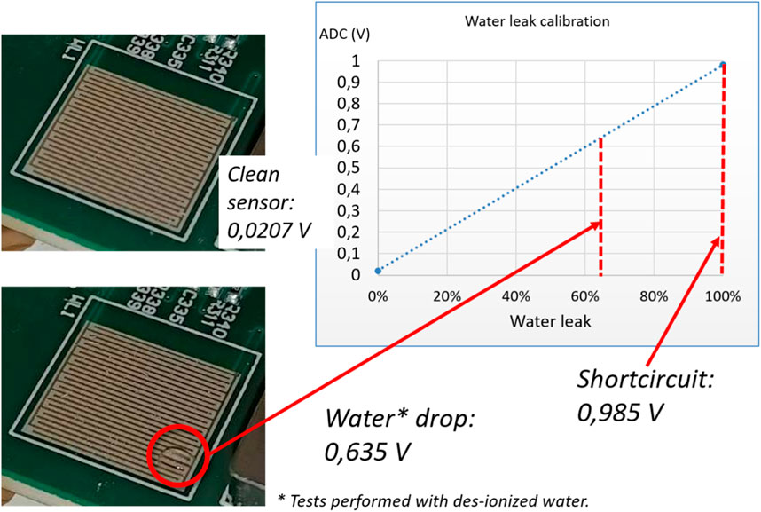
Figure 6. Image of the water leak sensor designed for the OBDT-theta with and without a water drop. In addition, the measured values in the ADC of the output of the water leak sensor electronics can be seen for both dry and wet situations.
Other slow control interfaces are implemented directly on the Polarfire FPGA and provide:
- Up to four independent I2C interfaces to connect to external devices. In CMS this could accommodate the connection to the FEBs, the Pressure Analog-to-Digital Conversion (PADCs), the alignment or the secondary slow control of the RPC (Resistive Plate Chambers).
- Generation of the Testpulse signal and eventually, also the generation of FEBs signal masks to create artificial geometrical patterns in the detector through the Polarfire.
2.5 Readout and firmware considerations
Apart from the aforementioned time digitization module, the FPGA firmware carries out several other tasks related to the data flow or control and monitoring of other boards or detector elements. A diagram of the different interconnections inside the OBDT-theta firmware can be seen in Figure 7.
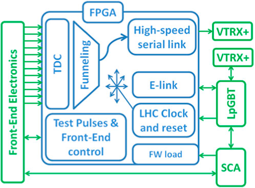
Figure 7. Diagram of the different interconnections inside the OBDT-theta firmware.
The data that is generated in the time digitization module needs to be delivered to the data backend via high-speed serial links. Given that data from the 228 input channels is stochastic, it cannot be ruled out that all channels provide data simultaneously, thus requiring to temporarily store and funnel it to the buffers of the output links. The maximum average single-channel input rate is 1 MHz, which corresponds to the maximum output rate of the FEB, resulting in an average output data rate of 5 Gbps. However, physics rates during HL-LHC are expected to be around 50 kHz per channel, for a final payload data rate well under 1 Gbps. The readout module must also enforce a maximum latency threshold in the delivery of the hits, as late hits cannot be used downstream in the trigger systems. As mentioned before, the output data is sent over a 10.24 Gbps serial link using the lpGBT protocol.
In addition, a secondary slow control bidirectional link using the lpGBT protocol was developed inside the Polarfire. Although this slow control link is actually an FPGA to FPGA link, it was decided to use the same lpGBT protocol, such that the backend is agnostic of whether we are connecting the primary or the secondary slow control.
Due to the characteristics of the VTRX+, whose receiver link is limited to a maximum speed of 2.56 Gbps (CERN, 2025), a custom version of the protocol had to be deployed in the Polarfire, as the lpGBT protocol repositories implement the receiver link for the backend case, i.e., with line rates inverted with respect to the ones needed in the OBDT.
Several functions in the OBDT board are either controlled or monitored by the firmware. I2C links exist between the FPGA and the two main other ASICs, SCA and lpGBT. The flow of the control signals has been designed such that most of the board functions can be controlled from both the FPGA and lpGBT. One of the two VTRX+ optical modules present in the board, the one that delivers the output data, is also controlled via I2C protocol by the FPGA to enable links or set configuration parameters.
The firmware can also control, by means of the I2C protocol, four other on-detector systems: DT FEBs, alignment, PADCs and RPCs. Finally, the FPGA firmware is also in charge of the management of the TestPulse-Theta board control signals.
2.6 Testpulses-theta board
The Testpulses-theta board allows performing the timing calibration of the wires in the theta SuperLayer of a DT chamber. The FEBs inside the DT chambers are built so that they can generate emulated signals as if they were coming from the anode when a pulse is injected at the early stages of its chain. Hence, a testpulse input to a FEB is passively forked in 16 channels within the FEB board, inducing a hit-like response from all 16 channels of a FEB. The starting (i.e., the falling) edge of the testpulse-signal must be steep enough to ensure a time-precise response of the FEB.
Furthermore, the FEBs are combined in pairs, where each pair shares the same coaxial-input at the DT-chamber casing panel. This results in 32 frontend channels generating a response when receiving a testpulse-signal at the respective coaxial-input of the DT-chamber. Taking into account the passive forking of the testpulse-signals within the DT-chamber and the requirement of the steep edge of the testpulse-signal, the driver of the testpulse-signal must deliver sufficient current.
To cover all the FEBs of a Theta-SuperLayer, the Tespulse-theta board contains eight coaxial connectors, providing eight synchronous testpulse-signals. The block-structure of the test-pulse board is shown in Figure 8. The pulses amplitude generated by the Testpulses-theta board can be adjusted and they have a steep falling edge at each output channel.
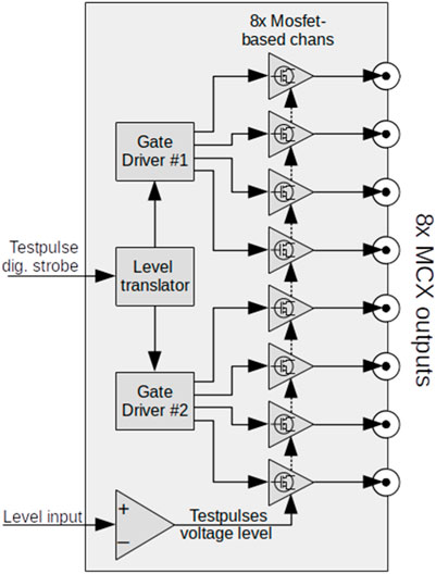
Figure 8. Diagram of the overall structure of the Testpulses-Theta board.
The FEB responses, induced by the injected testpulses are received and time-tagged by the OBDT-Theta. When repeating a testpulse-signal generation many times and provided no correlated interferences are present in the frontend chain, the time-tagged FEB-responses form a normal distribution, representing the jitter of the chain. The center of this normal distribution is used for the timing calibration of the chain delay. The developed Testpulse-theta board provides a rather sharp jitter-distribution, which is generally below the time-resolution of the TDC (Time to Digital Converter). A cumulative jitter plot, summarizing the responses from a cluster of 32 channels, is shown in Figure 9.
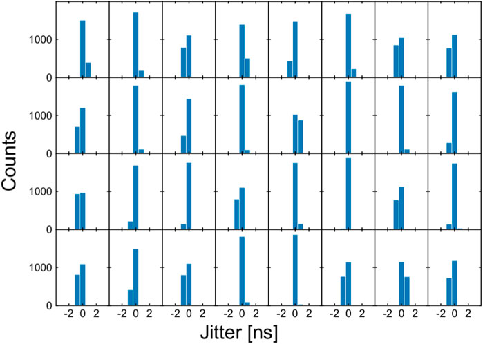
Figure 9. Jitter plots responses from a cluster of 32 FEB channels, which all respond to testpulse-signals from one common testpulse-input. Each plot is based on 1888 hit-like responses from the FEBs, which are then simultaneously time-tagged by the OBDT-Theta. One bin corresponds to 0.78 ns, reflecting the TDC time resolution. In each plot, the bin with the highest number of counts is aligned to 0. The measurement was conducted at the DT chamber within a DT test stand at RWTH Aachen.
2.7 Board design and mechanical assembly
The OBDT-theta has been designed in Panasonic Megtron 6 halogen free material with a 14 layers stack up. The PCB dimensions are 29 × 9 cm. The high speed tracks have been designed following special rules to ensure its optimal performance. Bit error rate tests executed on the board guarantee BER values below 10−13 in all the 10.24 Gbps links.
The cooling of the board can be achieved in several ways, but in an environment like the CMS detector, the dissipation needs to happen through a water cooling circuit at 17°C. Contact with this circuit will occur through an aluminum structure called frame. This frame has been designed to ensure the proper cooling of the most sensitive devices. In particular, the regulators, the FPGA, the transceiver and the VTRX+ are the most important hotspots that need to be in contact with a cold surface. The frame surface is machined with blocks of different heights, which have been calculated to ensure a proper force on each component when the OBDT-theta is screwed to the frame. The height of each component after assembly in the OBDT-theta has been measured with a profilometer. A thermal pad, SARCON® GR14B-0H-150PK, is used between each block and the OBDT-theta components to optimize the thermal contact while avoiding electrical shorts. Thermal simulations confirmed that no point in the board should be heated above 45°C.
On the other hand, the VTRX+ does not only need to be cooled down, but also its optical fibers need to be routed outside of the frame. A 3D piece was designed to appropriately route the extra length of the VTRX+ fibers. It also serves as support of the VTRX+ modules to prevent its bending or its connector damage. Figure 10 shows an image of this 3D piece.
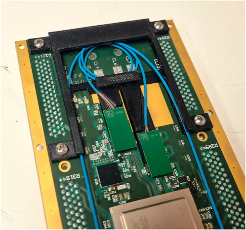
Figure 10. Image of the black 3D printed piece (PETG) attached to the bottom side of the OBDT-theta and supporting the two VTRX+ connected to the board. The 3D piece facilitates the routing of the VTRX+ optical fiber pigtails.
3 Validation at the laboratory
The OBDT-theta board has been extensively validated in the laboratory. An image of the board under testing can be seen in Figure 11. Its functionality has been tested in standard operation conditions and also its performance malfunctioning (short circuit, overvoltage, etc.) has been evaluated. Some of the test results are shown in the following.
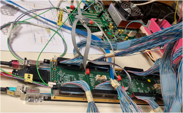
Figure 11. Image of the OBDT-theta board under testing at CIEMAT’s laboratory. An AMD VCU118 evaluation board is used as backend and custom-built boards are used to fan-out the signals and verify the different interfaces.
3.1 Differential non linearity
The Differential Non-Linearity (DNL) of the TDC has been measured using a code density test. This method consists of injecting signals that are synchronous to an external clock that is not correlated with the FPGA clock. In this way, the signals arrive at a random position, thus scanning all the time bins of the TDC with enough statistics. In the ideal scenario, a flat distribution over all the bins of the fine time measurement should be obtained.
The signal for the code density test has been generated by an evaluation board running on an independent clock source that injects a signal into some custom fan-out boards. These later boards could replicate asynchronously the signal into up to 256 differential channels and inject it into the OBDT-theta.
Figure 12 shows the distribution of the fine time measurements obtained. It can be observed that it is rather flat, with a DNL in the order of 10% (or 0.1 LSB). Also, the DNL shows a component of odd versus even bins that we believe is correlated with a non-perfect 50% duty cycle of the incoming clock.
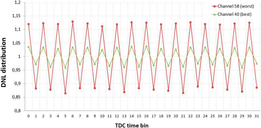
Figure 12. Image of the DNL in LSB versus the time bin obtained for two channels in the OBDT-theta: channel 58 with the worst DNL results and channel 40 with the best ones.
Figure 13 shows the DNL distribution of all the channels, indicating that the dispersion among all channels is small. Finally, in Figure 14, the results of the Integral Non Linearity (INL) for the worst channel and the best channel are shown.
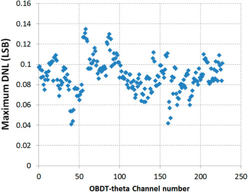
Figure 13. Distribution of the maximum value of the DNL over the 32 bins of each channel in the OBDT-theta. As can be seen, the average DNL is in the order of 10%.
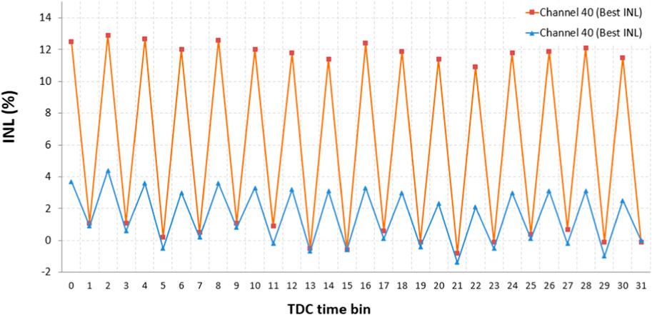
Figure 14. Image of the INL in percentage value versus the time bin obtained for two channels in the OBDT-theta: channel 87 with the worst INL results and channel 40 with the best ones.
3.2 Non stability of the time measurements
One aspect to consider is the potential metastability that could occur at the inputs of the OBDT-theta due to the asynchronous nature of the input pulses from the FEBs. Metastability in sampling analog pulses with a deserializer occurs due to timing uncertainties when the analog signal is converted into discrete digital samples. If the rising edge of the pulse arrives close to a deserializer decision threshold during a clock edge, the circuit may struggle to resolve a clear high or low state, leading to an undetermined output condition. This metastable state, characterized by prolonged, oscillatory behavior, can propagate through subsequent digital stages, potentially causing errors or unpredictable system performance. Figure 15 shows laboratory measurements with the OBDT-theta where no metastability was observed. The measurements were performed with different lengths of the input hit cable, to cover potential delay shifts. As can be seen, no effect of metastability has been observed.
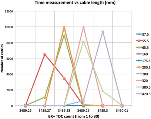
Figure 15. Results from the metastability tests at the laboratory performed by measuring a large number of times the same signal, synchronous to the OBDT-theta clock. In the horizontal axis different time bins are represented, while in the vertical axis is represented the number of times each time bin has been measured. The measurement has been repeated by increasing the length of the cables (in mm) transmitting this signal and the cable length for each represented line is indicated in the legend. This increase of lengths adds a delay to the signal according to the cable speed, which is roughly 5 ns/m. This test allowed to scan a wide region of time measurements around a time bin and no effect of metastability was observed.
Another point of concern is ensuring that each time a clock distribution disruption occurs, we can still continue performing reliable time measurements, assigning the same time stamp to the same signal. We have observed that clock distribution disruptions due to unlocks of the lpGBT links can be reliably recovered. We also observed that power cycling the board could cause some time measurement shifts and the results from testing this in the laboratory are shown in Figure 16. As can be seen, the time measurements differences that we observe are very small and much smaller than our required resolution of 0.78 ns.
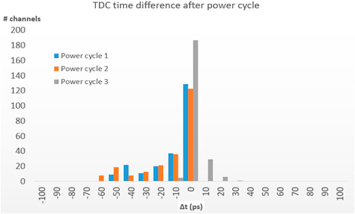
Figure 16. Results of the potential time difference measurement as a consequence of performing power cycles in the OBDT-theta board. As can be seen, the time measurements differences observed are very small and much smaller than our required resolution of 0.78 ns.
4 Conclusion
A readout board that performs the time digitization of up to 228 channels with a time bin of 0.78 ns has been developed at CIEMAT. This board performs the funneling and transmission of the data stream through a high speed optical link at 10.24 Gbps. A total bandwidth of at least 48 Gbps of payload is available at the board for data readout, much larger than the required one for the CMS DT chambers. The board was designed with components that are expected to safely withstand a radiation of up to 10 Gy and was built using halogen-free PCB material. Beyond its readout functionality, it provides slow control links for several systems of the DT chambers, including a board generating calibration signals developed by the Aachen group.
Up to 5 prototypes were built and tested in the laboratory, showing very good results and enabling us to validate the chosen design and architecture. It is expected that this board can be used very efficiently in the CMS DT detector for reading out the signals of the DT chambers during its operation in HL-LHC.
Data availability statement
The raw data supporting the conclusions of this article will be made available by the authors, without undue reservation.
Author contributions
CB: Conceptualization, Funding acquisition, Investigation, Project administration, Writing–original draft. SC: Conceptualization, Investigation, Validation, Writing–review and editing. JC: Conceptualization, Investigation, Writing–review and editing. DE: Conceptualization, Investigation, Software, Validation, Writing–original draft. NE: Data curation, Software, Writing–review and editing. DF: Conceptualization, Validation, Writing–review and editing. AN: Conceptualization, Investigation, Software, Validation, Writing–review and editing. RP: Investigation, Software, Validation, Writing–review and editing. CP: Conceptualization, Investigation, Software, Validation, Writing–review and editing. IR: Funding acquisition, Project administration, Resources, Validation, Writing–original draft. DR: Investigation, Software, Validation, Writing–review and editing. JS: Conceptualization, Investigation, Software, Validation, Writing–review and editing.
Funding
The author(s) declare financial support was received for the research, authorship, and/or publication of this article. This work is supported by the Ministerio de Ciencia e Innovación (Spain) and Bundesministerium für Bildung und Forschung (Germany). Grants PID2020-116262RB, research supporting program “ErUM-FSP T03” funded by MICIU/AEI/10.13039/501100011033, and Bundesministerium für Bildung und Forschung (Germany) and additional grants funded by the “European Union NextGenerationEU/PRTR”.
Acknowledgments
We gratefully acknowledge the enduring support provided by the “Agencia Estatal de Investigación”, the “Ministerio de Ciencia e Innovación” from Spain and “Bundesministerium für Bildung und Forschung” from Germany.
Conflict of interest
The authors declare that the research was conducted in the absence of any commercial or financial relationships that could be construed as a potential conflict of interest.
The author(s) declared that they were an editorial board member of Frontiers, at the time of submission. This had no impact on the peer review process and the final decision.
Generative AI statement
The author(s) declare that no Generative AI was used in the creation of this manuscript.
Publisher’s note
All claims expressed in this article are solely those of the authors and do not necessarily represent those of their affiliated organizations, or those of the publisher, the editors and the reviewers. Any product that may be evaluated in this article, or claim that may be made by its manufacturer, is not guaranteed or endorsed by the publisher.
Footnotes
1In the CMS coordinate system the x axis points towards the LHC center, while the z axis points to the Jura mountains, and the y-axis points toward the sky. In spherical coordinates, the azimuthal angle φ represents the angle on the xy plane (measured from the x-axis) and the polar angle represents the angle on the zy plane (measured on the z-axis).
References
Apollinari, G., Béjar Alonso, I., Brüning, O., Fessia, P., Lamont, M., Rossi, L., et al. (2017). High- luminosity large hadron collider (HL-LHC): technical design report V.0.1. doi:10.23731/CYRM-2017-004
Caratelli, A., Bonacini, S., Kloukinas, K., Marchioro, A., Moreira, P., Oliveira, R. D., et al. (2015). The GBT-SCA, a radiation tolerant ASIC for detector control and monitoring applications in HEP experiments. J. Instrum. 10 (C03034), C03034. doi:10.1088/1748-0221/10/03/c03034
CERN (2025). Versatile link plus project. VTRX+ module. Available at: https://espace.cern.ch/project-Versatile-Link-Plus/SitePages/Home.aspx.
CMS Collaboration (2017). The phase-2 upgrade of the CMS muon detectors. CERN-LHCC-2017-012; CMS-TDR-016. Available at: https://cds.cern.ch/record/2283189?ln=es.
CMS Collaboration (2020). The phase-2 upgrade of the CMS level-1 trigger technical design report. CERN-LHCC-2020-001. Available at: https://cds.cern.ch/record/2714892?ln=es.
Guettouche, N., Baron, S., Biereigel, S., Hernandez Montesinos, D., Kulis, S., Vicente Leitao, P., et al. (2022). The lpGBT production testing system. J. Instrum. 17, C03040. doi:10.1088/1748-0221/17/03/c03040
Hegeman, J., Andre, J. M., Behrens, U., Branson, J., Chaze, O., Cittolin, S., et al. (2015). “The CMS timing and control distribution system,” in 2015 IEEE Nuclear Science Symposium and Medical Imaging Conference (NSS/MIC), San Diego, CA, October 31–November 07, 2015 (IEEE), 1–3. doi:10.1109/NSSMIC.2015.7581984
Keywords: LHC, CMS, HL-LHC, phase-2, read-out, drift tubes, TDC
Citation: Bedoya CF, Cuadrado S, Cuchillo J, Eliseev D, Esper N, Francia D, Navarro A, Paz R, Presser C, Redondo I, Redondo DD and Sastre J (2025) OBDT-theta, a multi-channel TDC and readout board for the CMS muon drift tubes in HL-LHC. Front. Detect. Sci. Technol 3:1517241. doi: 10.3389/fdest.2025.1517241
Received: 25 October 2024; Accepted: 20 January 2025;
Published: 12 February 2025.
Edited by:
Gianluca Traversi, University of Bergamo, ItalyReviewed by:
Fernando Carrio Argos, University of Valencia, SpainImma Riu, Institute for High Energy Physics, Spain
Roberto Ferrari, National Institute of Nuclear Physics of Pavia, Italy
Copyright © 2025 Bedoya, Cuadrado, Cuchillo, Eliseev, Esper, Francia, Navarro, Paz, Presser, Redondo, Redondo and Sastre. This is an open-access article distributed under the terms of the Creative Commons Attribution License (CC BY). The use, distribution or reproduction in other forums is permitted, provided the original author(s) and the copyright owner(s) are credited and that the original publication in this journal is cited, in accordance with accepted academic practice. No use, distribution or reproduction is permitted which does not comply with these terms.
*Correspondence: I. Redondo, aWduYWNpby5yZWRvbmRvQGNpZW1hdC5lcw==