 Karthikeyan Nagarajan
- School of Electrical Engineering and Computer Science, State College, Pennsylvania State University, University Park, PA, United States
Hardware Trojans in Integrated Circuits (ICs), that are inserted as hostile modifications in the design phase and/or the fabrication phase, are a security threat since the semiconductor manufacturing process is increasingly becoming globalized. These Trojans are devised to stay hidden during standard structural and functional testing procedures and only activate under pre-determined rare conditions (e.g., after a large number of clock cycles or the assertion of an improbable net). Once triggered, they can deliver malicious payloads (e.g., denial-of-service and information leakage attacks). Current literature identifies a collection of logic Trojans (both trigger circuits and payloads), but minimal research exists on memory Trojans despite their high feasibility. Emerging Non-Volatile Memories (NVMs), such as Resistive RAM (RRAM), have special properties such as non-volatility and gradual drift in bitcell resistance under a pulsing voltage input that make them prime targets to deploy hardware Trojans. In this paper, we present two delay-based and two voltage-based Trojan triggers using emerging NVM (ENTT) by utilizing RRAM’s resistance drift under a pulsing voltage input. Simulations show that ENTTs can be triggered by reading/writing to a specific memory address N times (N could be 2,500–3,500 or a different value for each ENTT design). Since the RRAM is non-volatile, address accesses can be intermittent and therefore stay undetected from system-level techniques that can identify continuous hammering as a possible security threat. We also present three reset techniques to de-activate the triggers. The resulting static/dynamic power overhead and maximum area overhead incurred by the proposed ENTTs are 104.24 μW/0.426 μW and 9.15 μm2, respectively in PTM 65 nm technology. ENTTs are effective against contemporary Trojan detection techniques and system level protocols. We also propose countermeasures to detect ENTT during the test phase and/or prevent fault-injection attacks during deployment.
1 Introduction
Integrated Circuits (IC) are vulnerable against malicious modifications in the form of Hardware Trojans (Bhunia and Tehranipoor, 2018) which can cause the ICs to perform a range of undesirable operations post deployment. Hardware Trojans are ideally designed to evade pre-silicon verification and post-silicon test. They are designed to remain dormant during the test phase and be triggered only under the activation of a rare net/condition. Recently surfaced news regarding top US companies like Amazon and Apple being affected due to the tampering of server motherboards by certain Chinese manufacturers (Robertson and Riley, 2018) provides a strong incentive to explore the risk of introducing malicious hidden components during either the design or the manufacturing phase of ICs.
In the past, multiple papers have explored and proposed possible hardware Trojans, including their triggers and payloads. A ‘content and timing’ based Trojan trigger, proposed in (Test Time, 2018), is activated only when a pre-determined pattern is input at a specific time by the adversary. The Trojan, which is implemented in a Basys FPGA Board, evades testing routines even when a correct trigger pattern is fed as input since timing constraints may not be met. In (Hoque et al., 2018), a Trojan, whose activation depends on writing a specific pattern to one/few cells, is proposed for an embedded SRAM. Once the pre-determined pattern is written to the cells (acts as a trigger), the Trojan transistors (payload), which are controlled by the trigger signal, are activated. The paper proposes using an input pattern that does not feature in conventional testing. But, when random input patterns are applied during functional tests and Burn-in, there exists a non-trivial possibility of activating the Trojan and revealing its presence. Additionally, the practicality of the Trojan is limited due to the challenging nature of inserting the Trojan transistors at an SRAM internal node due to its compact bitcell footprint. This Trojan is also only applicable for charge-based memories such as, as SRAM and DRAM, since the charge stored at data nodes can be leveraged to activate Trojan transistors. The design proposed in (Hoque et al., 2018) is incompatible with emerging Non-Volatile Memories (NVM) which rely on cell resistance/material magnetization to represent stored data.
An efficient Trojan is small, controllable and undetectable. In (Yang et al., 2016), an analog Trojan trigger named A2 is presented. It is a controllable, stealthy and small capacitor-based trigger that, when activated, inverts specific control-logic bits and escalates the adversary’s privilege in the system. If A2 is extended to a memory/NVM-based trigger, it is capacitor value will have to be prohibitively high to endure a high number of address accesses (hammerings) to remain undetected during testing. In (Khan et al., 2019), a capacitive Trojan trigger is proposed that activates when a pre-determined data input is written to a pre-determined memory address and another pre-determined memory address is accessed a large number of times. The capacitor value employed in this work is high (∼ 100 fF) enough to endure a large number of address accesses (∼ 260, denoted by Ntr in this work) that is needed to evade the test phase. But this large capacitor increases the circuit footprint that makes the Trojan detectable during optical testing. Moreover, the Trojan is not controllable by the adversary and auto-resets (after 52.39 µs) once the address accesses are stopped.
Motivation for Emerging Non-Volatile Memories-Based Trojan Triggers
Existing NVM Trojan triggers have certain shortcomings. Pattern based Trojans such as, (M. N. I. Khan et al., 2019), may get triggered inadvertently while A2-based triggers (K. Yang et al., 2016), when extended to NVM, are constrained by large capacitors that are detectable. Emerging NVMs possess unique qualities that can be leveraged to overcome such restrictions while presenting minimal energy and area overheads. In the case of Resistive RAM (RRAM) (Chen et al., 2015) and phase Change RAM (PCRAM) (Kim et al., 2011), the bitcell resistance drifts gradually in accordance with the pulsing voltage input (i.e., width and frequency of pulses).
In Figure 1, it is shown that the RRAM bitcell’s (employed in this work) resistance grows by 2.21 Ω each time a 2ns pulse of 1.2 V is applied across the bitcell. This gradually drifting resistance, caused by repeated hammering with 1.2 V pulses, can be leveraged to generate a trigger signal that can deliver a payload. Trigger circuits using the unique qualities of emerging NVM, such as, RRAM’s gradual resistance drift, can be exploited by adversaries due to, 1) need of small footprint (ENTTs proposed in this paper require at most 9.15 μm2) making them hard to detect during the test phase; 2) requirement of a large number of hammering pulses to assert the trigger (Ntr = 2,500 to 3,500 in this work); and 3) possession of controllability over the attack initiation, duration, and reset i.e., the malicious payload allows activation and de-activation at will of the adversary. Here, Ntr refers to the number of times a specific pre-selected address has to be accessed in order to activate the Trojan trigger.
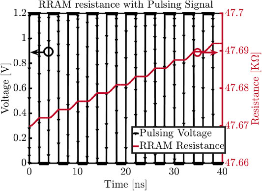
FIGURE 1. Drift of RRAM resistance with pulsing signal (Nagarajan et al., 2019).
ENTT and the Attack Model: The paper presents four RRAM-based Trojan trigger circuits, two of which are based on delay sensing (ENTT-1 in Figure 2A and ENTT2 in Figure 2B), and two others based on voltage sensing (ENTT-3 in Figure 2C and ENTT-4 in Figure 2D). While ENTT-1 and ENTT-3 are presented in (Nagarajan et al., 2019), we have proposed two new designs in ENTT-2 (delay-based) and ENTT-4 (voltage-based) to provide critical improvements in trigger power consumption. .
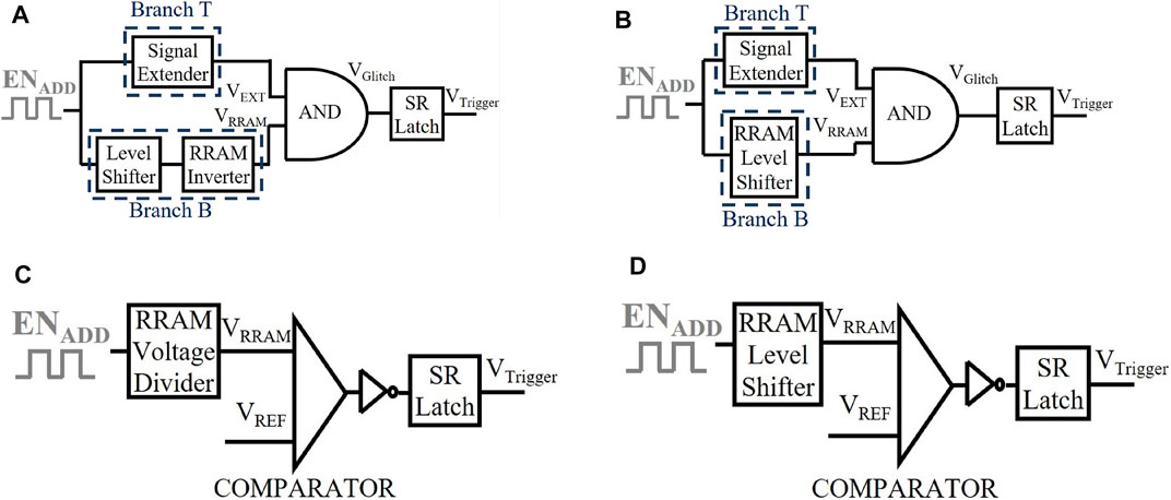
FIGURE 2. (A) ENTT-1, (B) ENTT-2, (C) ENTT-3, and (D) ENTT-4. A level shifter is needed since RRAM requires 2.2 V.
Each ENTT takes a pre-determined address enable signal (ENADD) as its input and outputs a trigger signal (VTrigger) that delivers a malicious payload. VTrigger switches from low to high when the specific address is accessed (written or read) at least Ntr times. ENTTs (and other Trojan triggers) can be maliciously inserted into an IC either during the design or fabrication phase. By designing the ENTTs with a high Ntr, through appropriate selection of RRAM’s initial resistance and ENTT design, the triggers can pass randomized functional testing and traditional March testing without detection. In order to activate/reset the trigger, the adversary would need to hammer a pre-selected address (details in Sections 3–6).
Note that the proposed Trojan triggers do not require continuous address accesses since the RRAM is inherently non-volatile and preserves its incremental change in resistance. This allows the attacker to conceal the repeated accesses by only intermittently accessing the pre-determined memory address and hide from system-level hammering detection techniques.
A brief outline of each of the proposed trigger circuits (ENTT 1–4) and reset circuits (ENTTR 1–3) are presented below:
ENTT-1 and ENTT-2 (Delay-Based): The resistance drift observed in RRAM during address hammering is leveraged by these triggers to introduce an increase in path delay which is then used to generate a glitch. The ENADD signal, that is used for hammering, is the decoded signal for a specific address. Therefore, ENADD is pulsed each time the pre-selected signal is accessed. This decoded ENADD pulse is fed into two branches, named as Branch T (Top) and Branch B (Bottom) of ENTT-1 (Figure 2A). In Branch T, an inverted signal (VEXT) of ENADD with an extended ON period is generated (Figure 3). In Branch B, ENADD is delayed with no other modification to generate VRRAM (Figure 3). Whenever ENADD has a 0 → 1 shift, the resistance of the RRAM in the RRAM-Inverter increases. This causes the 1 → 0 shift of VRRAM to slow down (i.e. the falling edge is delayed). If the corresponding memory address is accessed Ntr times (ENADD has Ntr pulses), the VRRAM’s 0 → 1 switch is slowed down sufficiently to cause the AND gate to generate a glitch. If the width of the generated glitch is adequately wide (greater than the propagation delay of the SR latch), VTrigger is latched to HIGH. Note that an additional inverter (not shown) is inserted after the RRAM-inverter to ensure a clean output signal. ENTT-2 (Figure 2B) proposed, is similar to ENTT-1 except that we have combined RRAM inverter and level shifter circuit into a RRAM-level-shifter. The RRAM bitcell is essentially embedded into the level shifter. This saves leakage power of the trigger circuit by 4.84X.
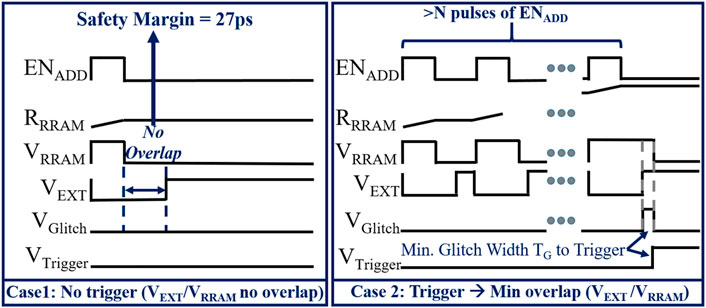
FIGURE 3. Glitch generation from outputs of Branch T and B(Nagarajan et al., 2019).
ENTT-3 and ENTT-4 (Voltage-based): The resistance drift observed in RRAM during address hammering is leveraged by these triggers to introduce a voltage change at a specific node that is then leveraged by a voltage comparator to generate the trigger signal. ENTT-3 (Nagarajan et al., 2019) utilizes a resistance divider between NMOS/PMOS transistors and a RRAM bitcell. The RRAM’s resistance increases each time ENADD is asserted. This causes the voltage of the node between the RRAM and the NMOS/PMOS to correspondingly drop. This node voltage is fed into a comparator with a pre-determined reference voltage as the other input. If the node voltage drops under the reference voltage, the output of the comparator shifts from 1 to 0. This 0 (LOW) signal is then inverted and finally captured by an SR latch. ENTT-4 uses a similar circuit as ENTT-3, except the voltage divider is embedded in the level shifter. It is shown that the leakage power of ENTT-4 is improved by 1.25X as compared to ENTT-3.
Resetting the trigger: We also propose three reset mechanisms which can be implemented for each of the proposed ENTTs. We call them ENTT Reset (ENTTR-1, 2 and 3). ENTTR allows the attacker to discontinue the attack (to stay undetected) and relaunch as desired. The ENTTR, in essence, allows the attacker to undo the RRAM resistance drift by hammering the RRAM in reverse polarity. This renders the proposed Trojan triggers to be highly controllable and undetectable.
Memory Trojan Payloads: When the trigger is activated, it causes the VTrigger to be asserted. This trigger signal is then used to launch malicious payloads such as information leakage attacks, Denial of Service (DoS) attacks, and fault injection attacks. The exploration of payloads is brief in this work since memory Trojans payloads have already been detailed in prior works (Chakraborty et al., 2009; Khan et al., 2019; Nagarajan et al., 2019).
Specifically, we have made the following contributions in addition to (Nagarajan et al., 2019). We, 1) proposed a new delay-based Trojan trigger (ENTT-2) and a new voltage-based Trojan trigger (ENTT-4) by leveraging RRAM resistance drift; 2) provided analysis of new triggers to show lower power consumption compared to prior work (Nagarajan et al., 2019); 3) proposed two new Trojan reset mechanisms (ENTTR-2 and ENTTR-3); 4) performed design space exploration of the newly proposed trigger circuitry; 4) presented process variation analysis for the newly proposed ENTTs to confirm that the trigger stays inactive during the test phase even under worst-case corners; 5) proposed new Error Correcting Code (ECC)-based countermeasure for the proposed ENTTs and overhead analysis.
The paper is organized as follows: Section 2 provides a background of RRAM; Sections 3 describes the delay-based and voltage-based ENTTs; Section 4 presents the proposed resetting mechanisms of the Trojan triggers; Section 5 proposes countermeasures against the proposed triggers; Section 6 presents a discussion on the practicality, assumptions and limitations of the proposed trigger circuits; Finally, Section 7 draws the conclusion.
2 Background on Resistive RAM
2.1 Basics of Resistive RAM
An RRAM bitcell consists of oxide material between its Top Electrode (TE) and Bottom Electrode (BE) as shown in Figure 4. Its resistive switching is caused due to oxide breakdown (leading to high resistance) and re-oxidation (leading to low resistance) of the conductive filament (CF). The RRAM gap is defined as the distance between the top electrode and the tip of the CF. By applying a positive/negative voltage on the RRAM device, the gap will decrease/increase due to the generation/recombination of oxygen vacancies at the tip of CF. The CF allows the transportation of electrons in its oxygen vacancies through electron hopping. The atomic hopping distance is defined as the distance between primary electron donor and final electron acceptor. This distance is split into a series of short steps. RRAM’s two resistive states are named as High Resistance State (HRS) and Low Resistance State (LRS). The operation of switching the RRAM’s state to LRS (HRS) is termed as SET (RESET). Further details regarding the operation of the RRAM model implemented in this paper can be found in (P. Y. Chen et al., 2015).
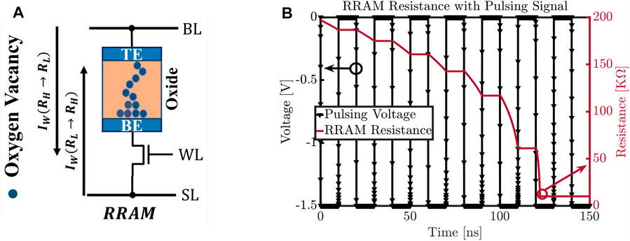
FIGURE 4. (A) RRAM bitcell; and, (B) RRAM resistance drift (negative) with reverse pulsing signal (Nagarajan et al., 2019).
2.2 Resistive RAM Resistance Drift
In Figure 1, it is shown that the RRAM resistance gradually increases as a pulsing voltage signal is applied across its electrodes. Correspondingly, in Figure 4B, it is shown that the RRAM resistance can be decreased if the polarity of the pulsing voltage signal is reversed. This work leverages this positive and negative resistance drift of RRAM to trigger the Trojan (launch the attack) and to reset the Trojan (exit the attack).
We have employed ASU’s RRAM Verilog-A model (Chen et al., 2015) and PTM 65 nm technology for our ENTT design and analysis. The RRAM used is a bipolar HfOx-based resistive switching memory (Chen et al., 2015). The model parameters used in this work are shown in Table 1. In this work, the initial resistance of the RRAM cells are set to 47.7 KΩ.
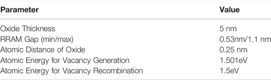
TABLE 1. RRAM parameters used for simulations.
3 ENTT Design and Analysis
3.1 Delay-Based Trojan Trigger
This section presents design and analysis of the delay-based Trojan triggers ENTT-1 and ENTT-2. We have performed detailed the design for ENTT-2 with critical improvements in leakage-power consumption (details in Section 6.1).
3.1.1 ENTT-1: Design and Analysis (Nagarajan et al., 2019)
ENTT-1 takes the tapped ENADD signal of a pre-selected address as its input and generates a trigger signal (VTrigger) as its output after the pre-selected address is accessed Ntr times (2,500–3,500) by the adversary. This trigger assertion is caused by a special RRAM-inverter module. Details regarding ENTT-1’s circuit architecture and design space exploration can be found in (Nagarajan et al., 2019).
3.1.2 ENTT-2: Design and Analysis
ENTT-1 proposes a voltage level shifter followed by a RRAM-inverter. We observe from ENTT-1 that contention helps to increase RRAM resistance. Therefore, for ENTT-2, we have embedded two RRAMs in the PMOS paths of a voltage level shifter (instead of using an RRAM-inverter) since it inherently contains a contention due to feedback connected PMOS. We call this design RRAM-voltage level shifter (Figure 5).
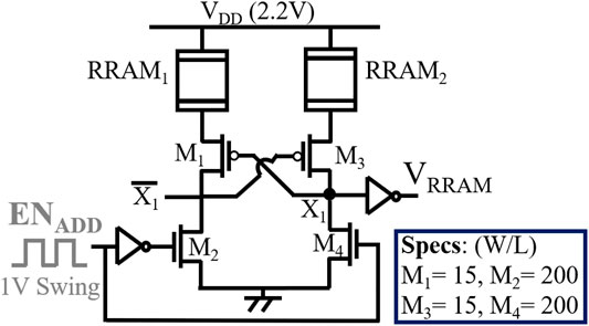
FIGURE 5. ENTT-2: Delay-based trigger.
Figure 6 shows that Ntr depends on the size of PMOS and NMOS in the level shifter. We have considered (W/L) = 20 and 150 for PMOS and NMOS respectively for Ntr = 3114. ENTT-2 design and operation is similar to ENTT-1 except the usage of RRAM-voltage level shifter. Figure 7 shows the timing waveform of Branch T, Branch B, VGlitch and VTrigger.1000-point Monte-Carlo analysis with 3σ of 5% of the RRAM’s initial resistance with a mean of 47.7 kΩ at T = 25C. Figure 8A and Figure 8B depict the process variation (PV) distribution of the number of address accesses (i.e. ENADD pulses) required to achieve 0.5 and 1 V of VGlitch respectively. Figure 8C depicts the PV distribution of the number of address accesses (Ntr) required for the SR latch to capture VGlitch. Here the worst-case scenario is the PV instance where ENTT-2 is triggered with the lowest Ntr. The lowest Ntr = 2120 observed for ENTT-2 under PV is large enough to stay undetected during testing.
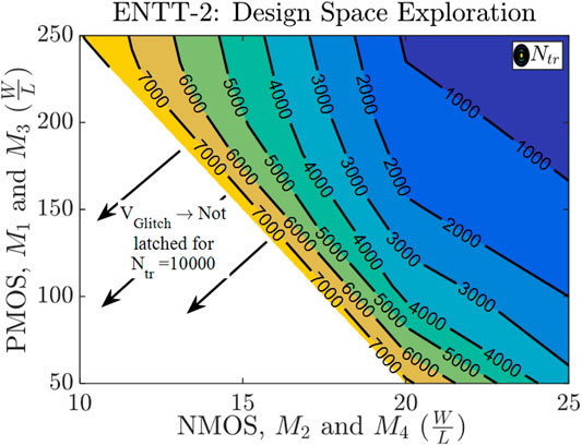
FIGURE 6. ENTT-2: Design space exploration.
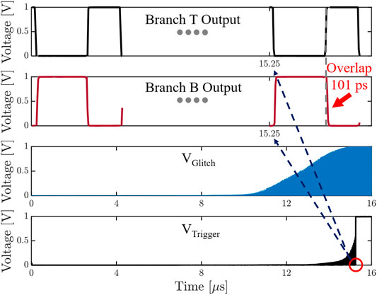
FIGURE 7. ENTT-2: Timing waveforms showing Branch T and B outputs, VGlitch and VTrigger.
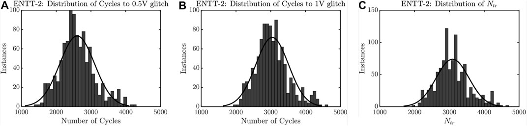
FIGURE 8. Process variation analysis of ENTT-2. (A), (B) and (C) shows the distribution of Ntr for VGlitch to reach 0.5 and 1 V and to capture VGlitch by the SR latch respectively.
3.2 Voltage-Based Trojan Trigger
We present voltage-based Trojan triggers namely, ENTT-3 (Nagarajan et al., 2019) and ENTT-4 by leveraging the change of resistance-divider-node voltage composed using RRAM after the resistance drift. The proposed ENTT-4 provides critical leakage-power consumption improvements (details in Section 6.1).
3.2.1 ENTT-3: Design and Analysis (Nagarajan et al., 2019)
ENTT-3 also takes the tapped ENADD signal as its input and generates a trigger signal (VTrigger) as its output. This trigger assertion is caused by a special RRAM-voltage divider and a voltage comparator. Further details regarding the RRAM voltage divider, and comparator design and space exploration can be found in (Nagarajan et al., 2019).
3.2.2 ENTT-4: Design and Analysis
ENTT-4 utilizes the RRAM-voltage level shifter and leverages the voltage division with respect to RRAM resistance to realize the trigger. We use the RRAM level-shifter designed for ENTT-2 as shown in Figure 5. The voltage drop across the RRAM bitcell is detected by feeding the VRRAM signal into the comparator circuit to be compared with the VREF (695 mV in this work) signal. Simulation results (Figure 9) indicate that we achieve a sense margin of 103 mV and ENTT-4 triggers with Ntr = 3312 for (W/L) of PMOS = 15 and NMOS = 200. Additionally, we conducted a 1000-point Monte-Carlo analysis with same setup as the previous ENTTs and prove that the worst case Ntr of 2,170 (Figure 10) evades the test phase.
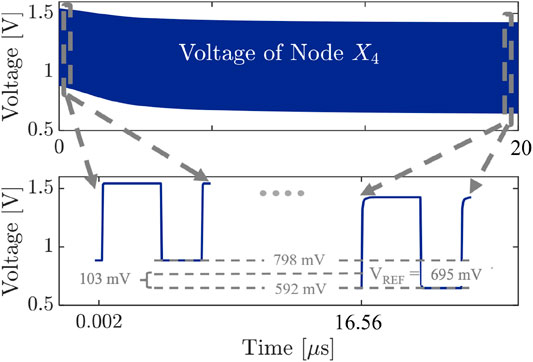
FIGURE 9. ENTT-4: Output of RRAM voltage divider embedded in level-shifter and sense margin of ENTT-4.
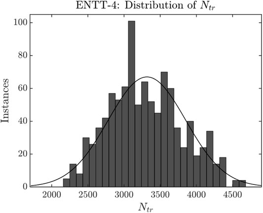
FIGURE 10. Process variation analysis of ENTT-4 to capture comparator output by the SR latch.
4 ENTT Reset Mechanisms
In order to ensure that the VTrigger signal stays asserted, we employ an SR latch. To ensure controllability and stealthiness of the ENTT designs, the adversary should be able reset the trigger at will. In this paper, we propose three reset circuits which mainly consists of two operations: 1) reset the RRAM resistance to its initial state (47.7Ω in this paper); and 2) reset the SR latch by generating a reset glitch.
4.1 Resetting the Resistive RAM Resistance
In order to reset the ENTT’s SR latch from 1 to 0, it is reset (R) input needs to be asserted. This can be achieved by generating a secondary glitch (i.e. reset glitch). However, VGlitch (for ENTT-1 and ENTT-2) can be generated again or the comparator (for ENTT-3 and ENTT-4) can output a “0” again due to a single read/write to the pre-selected address. This causes the output of the SR latch to be inadvertently SET again. Therefore, the RRAM resistance needs to be reset to its initial resistance (47.7 Ω) in order to completely disable the trigger. Once the RRAM resistance is reset, in order to restart the attack, the adversary will hammer the address again (for Ntr times) to change the RRAM resistance and re-assert VTrigger. Details regarding RRAM’s resistance reset operation are elaborated in (Nagarajan et al., 2019).
4.2 Resetting the SR Latch
In order to reset ENTT’s SR latch, a reset glitch needs to be generated and fed as R signal into the latch. We present 3 different mechanisms to reset the ENTTs:
1) Design and analysis of ENTTR-1 (for all ENTTs): A secondary circuit similar to the attack circuit (ENTT 1/2/3/4) can be used to generate the reset signal. Additional details regarding the operation of ENTTR-1 can be found in (Nagarajan et al., 2019).
2) Design and analysis of ENTTR-2 (applicable to only ENTT-2/ENTT-4): ENTT-2 inherently contains two RRAMs which can be leveraged to generate both set and reset signals of SR latch simultaneously. Figure 11 depicts the reset implementation using ENTTR-2. Adversary hammers address, ADD1 and the resistance of both RRAMs of ENTT-2 increases. VTrigger is asserted after Ntr = 3114 cycles of hammering and the attack starts. To stop the attack, the adversary hammers: 1) ADD2 for C1
The advantage of ENTTR-2 is that it incurs lower area overhead compared to ENTTR-1 when implemented for ENTT-2 and ENTT-4 since it does not require any additional reset RRAMs. Since both ENTT-2 and ENTT-4 utilize the same RRAM-voltage level shifter (Figure 5), ENTTR-2 can also be implemented for ENTT-4.
3) Design and analysis of ENTTR-3 (applicable to all ENTTs): We have shown in Figure 4B that the RRAM resistance reduces under a reverse pulsing current. We leverage this observation to propose ENTTR-3 (Figure 12) which is similar to ENTT-1 design except the RRAM terminals are flipped so its initial resistance is high. Therefore, VRRAM and VEXT will have an initial overlap and the NOR output of these two signal will be 0 (Figure 13).
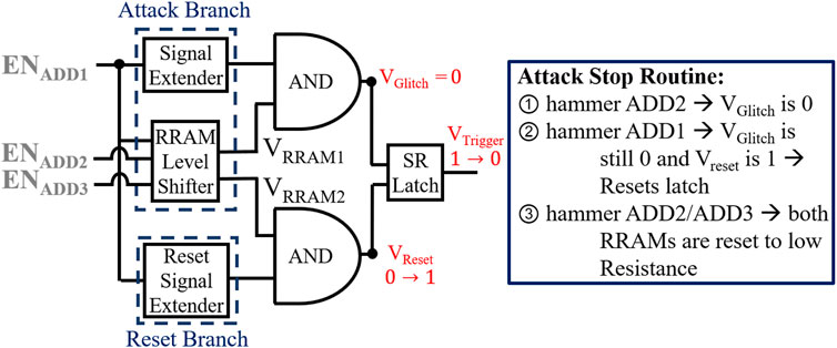
FIGURE 11. Implementation of ENTTR-2 for ENTT-2.
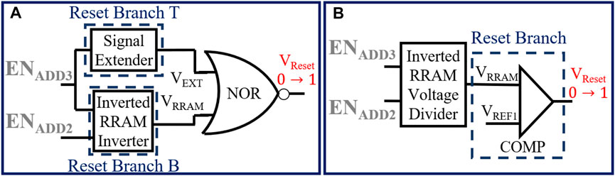
FIGURE 12. ENTTR-3 implementation for (A) ENTT-1 and 2; (B) ENTT-3 and 4.
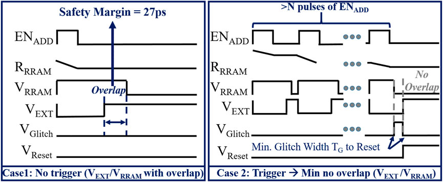
FIGURE 13. Reset glitch generation waveform for ENTTR-3.
However, the resistance of RRAM of ENTT-3 reduces as ADD1 is hammered and 1 → 0 transition of VRRAM becomes faster. Finally, 1 → 0 transition of VRRAM occurs before 0 → 1 transition of VEXT and both inputs to the NOR gate becomes low. Therefore, the NOR gate will output a 1 which is used to reset the SR latch. Interestingly, both set and reset signal can be generated simultaneously from ENTT-2 by flipping one of the RRAMs and keeping its resistance high initially. For ENTT-3/ENTT-4 (Figure 12B), one comparator is needed which has the VRRAM node pre-charged to ground. Only when the reset RRAM is hammered and its resistance is lowered, VRRAM node will charge more than the reference voltage and the comaparator outputs a 1. This can be used as reset signal for the latch. Note that this design has two RRAMs and therefore requires three ENADD to correctly set and reset the attack (similar to ENTT-1/2).
4.3 Overhead Analysis of ENTTR
The reset techniques as described above include: 1) resetting the RRAM resistance, and 2) generating the reset (R) signal for the SR latch. The power consumption to reset the 1 RRAM bitcell (in any ENTT) is equal to writing 1 bit of data to ‘0’ value. In a 0.5 GB RRAM memory array, there are 4 × 109 bits and therefore the power consumption for SET/RESET operations of 1 RRAM bit (from the ENTT) is negligible. Furthermore, generating the reset signal (R) incurs no additional circuitry for ENTTR-2. Therefore, the power and area overheads of the ENTTR-2 is negligible since we simply leverage the second RRAM that is already present in our ENTT-2/3 designs to generate the reset (R) signal for the SR latch. ENTTR-3 uses one additional block of any ENTT to gereate the reset signal. Therefore, the power and area overheads of ENTTR-3 are equal to the metrics of any one of the ENTTs as shown in Table 2.
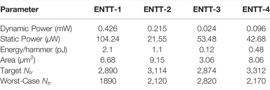
TABLE 2. Comparison of different ENTTs.
5 Countermeasures Against ENTT
ENTTs are designed to evade functional and structural testing. As detailed in (Nagarajan et al., 2019), they are effective against ATPG, Side Channel Analysis (SCA), detection by inspection, detection through March tests, wear leveling techniques, hammering detection routines, and detection by ECC. A few countermeasures such as, address scrambling, a small validated ECC, and analysis of memory images have also been described (Nagarajan et al., 2019). Here we propose two additional techniques, and validate their effectiveness through simulations.
1) Voltage/temperature modification to screen Trojan: Simulation results show that increasing the operating voltage (VDD) speeds up RRAM’s resistance drift. This causes the ENTT to be triggered earlier than adversary desires and be detected during the test phase. Similarly, simulations also indicate that increasing the temperature speeds up RRAM’s resistance drift. Figure 14 and Figure 15 show the effect of temperature and voltage variation respectively in each of the ENTTs.
2) ECC Scrambling: To prevent an attacker from adding malicious Trojans to tamper the ECC bits, we propose scrambling of the ECC columns between different address rows using hardware bit swizzling. Two cases are possible:
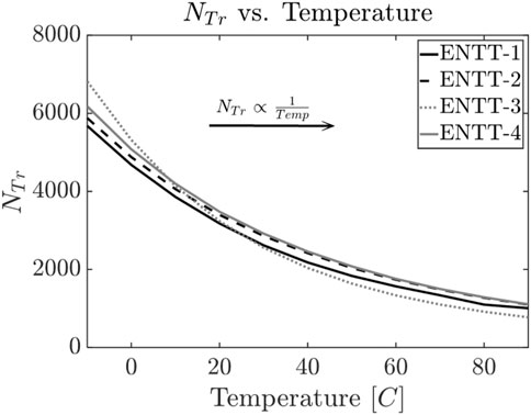
FIGURE 14. Effect on Ntr due to temperature variation.
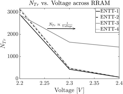
FIGURE 15. Effect on Ntr due to voltage across RRAM variation (at 25 °C).
Case 1: Hardwired swizzling.
Figure 16A shows hardwired swizzling of the ECC columns between neighboring 64-byte address lines. CASE-1 assumes that the adversary is in the design house and has access to the layouts. This case carries no area or power overhead.
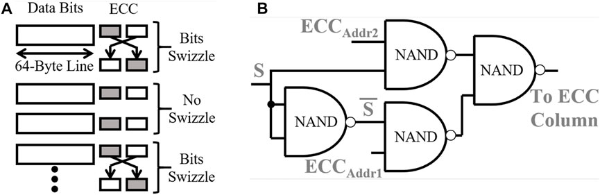
FIGURE 16. (A) ECC swizzle design to prevent corruption and ensure ENTT attack detection. (B) 2-input MUX implementation using NAND gates for ECC column selection. Addr1 and Addr2 represent 2 adjacent address rows.
Case 2: MUX controlled swizzling.
An adversary present in the fabrication house can examine the layout of the chip to detect any hardwired swizzling between the ECC bits. The adversary can then ensure that the right ECC bit is tampered to avoid ENTT attack detection. To address this concern, we propose a fuse-programmable swizzling. We implement two 2-input MUXes that take in the ECC bits of adjacent rows and stores them in two corresponding ECC columns depending on a “Select” bit (S) determined post fabrication. If the adversary fails to guess the select bit correctly, any fault in ECC and memory word will get detected due to scrambling. We have designed a 65-nm NAND implementation of the 2-input MUX as shown in Figure 16B. The W/L ratio of both the PMOS and NMOS transistors are set to 1. The average power consumed for all combinations of the 2 ECC bit inputs and Select Signal (S) is found to be 97nW and the total area overhead is 27.04 pm2.
6 Discussions
6.1 Comparison of ENTTs
Table 2 outlines critical performance metrics of each ENTT. We conclude that ENTT-1 is more power/area hungry compared to the others. Furthermore, the delay-based triggers (ENTT-1 and 2) are susceptible to process variation as compared to the voltage-based triggers (ENTT-3 and 4). Among the delay-based ENTTs (1 and 2), the newly proposed ENTT-2 reduces static power by 79.32%, and incurs an area increase of 36.9%. Among the voltage based ENTTs (3 and 4), the newly proposed ENTT-3 reduces static power by 25.3%, and incurs an area increase of 163%. Note that static power is the most critical metric in designing stealthy Trojan triggers since the Trojans lie dormant throughout the test phase. Therefore, reducing the static power reduces the risk of detection during testing through power side channel analysis. This static power for all ENTTs can be further significantly decreased by power gating the trigger using ENADD. Note that the static power overhead and the maximum area in the ENTTs proposed in (Nagarajan et al., 2019) are 104.24 μW and 6.68μm2, respectively. Among the newly introduced ENTT-2 and ENTT-4, the maximum area and static power overhead are 9.15μm2 and 42.68 μW respectively. Note that all of these values are less than 0.001% each considering typical memory area and static power (M. Chang et al., 2013). The area measurements for the proposed ENTT designs were calculated from their layout. Figure 17 depicts the layout schematic of the RRAM voltage level shifter block that has been implemented in the newly proposed ENTT designs. Note that, in addition to the area from the layout, the total area includes the area of the RRAM bitcells, and additional logic (e.g., inverter chains and/or comparators) which are hidden in the midlogic region (Bhattacharya et al., 2008) of the memory array.
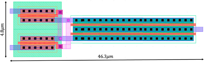
FIGURE 17. Layout schematic of the RRAM voltage level shifter block in the proposed ENTT-2 and ENTT-4 designs.
6.2 ENTT Comparison With Existing Literature
Table 3 presents the performance metrics of ENTTs under the worst-case scenario with previously published sequential triggers. In (T. Hoque et al., 2018), a trigger with significantly lower design overhead is presented. But, the trigger is activated after writing a specific pattern to a specific address just once. This trigger is also restricted to charge-based memories. Furthermore, bitcell modifications are practically infeasible in SRAM cells due to their high density.
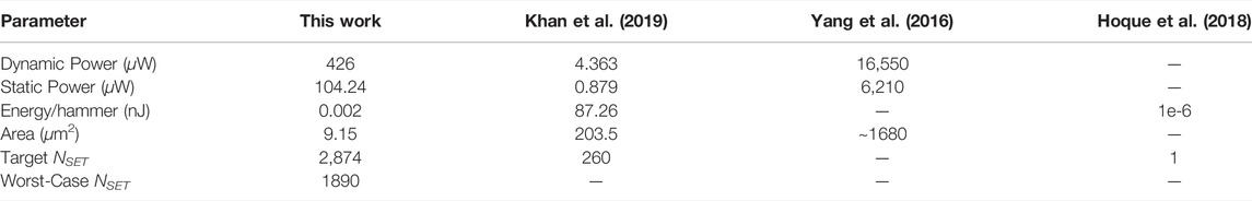
TABLE 3. Comparison of various Sequential Triggers (Nagarajan et al., 2019).
The ENTTs presented in this paper can be implemented for a wide range of NVMs. The ENTT’s dynamic and static power are higher by 97.6X and 118.6X respectively, but has a significantly lower area (0.06X) as compared to (Khan et al., 2019). Moreover, ENTTs incur 0.026X, 0.017X and 0.005X lower dynamic power, static power and area respectively as compared to (K. Yang et al., 2016).
6.3 Memory Trojan Payload
Payloads for memory trojans have been extensively studied and some key examples are shown in (Nagarajan et al., 2019). These payloads can mainly be categorized to deliver information leakage attacks, fault injection attacks, and denial-of-service attacks. These attacks can reveal sensitive data such as page-table information, allow attackers to perform differential fault analysis on cryptographic systems, and prevent write capabilities for a victim. For the sake of brevity, we restrict our discussion on the topic.
7 Conclusion
We proposed four different Emerging NVM Trojan Trigger (ENTT) designs by leveraging RRAM’s unique characteristics. These triggers have special features including, 1) the ability to start and end the attack at will, 2) a negligible area overhead to prevent detection using optical inspection, 3) avoiding detection through conventional testing due to need of a large number of pre-selected address accesses, and 4) evading system-level hammer detection techniques due to RRAM’s inherent non-volatility. We present the circuit, design space exploration, and process variation analysis of additional ENTT flavors that offer critical power improvements compared to previously proposed ENTT designs. Additionally, new novel reset mechanisms are presented for the proposed ENTTs. This attack surface can be potentially used to launch malicious payloads such as, DoS, fault injection, and information leakage attacks. Finally, effective countermeasures against all the ENTT flavors and their area/power overheads are presented.
Data Availability Statement
The original contributions presented in the study are included in the article/Supplementary Material, further inquiries can be directed to the corresponding author.
Author Contributions
KN; Responsible for idea conception, circuit level design, simulation, result generation. MI: Responsible for circuit design, debugging, figure generation, paper write up. SG: Responsible for idea conception, idea feasibility analysis, design debugging, result analysis.
Funding
This work is supported by SRC (2847.001 and 3011.001) and NSF (CNS-1722557, CCF-1718474, DGE-1723687, DGE-1821766, OIA-2040667 and DGE-2113839).
Conflict of Interest
The authors declare that the research was conducted in the absence of any commercial or financial relationships that could be construed as a potential conflict of interest.
Publisher’s Note
All claims expressed in this article are solely those of the authors and do not necessarily represent those of their affiliated organizations, or those of the publisher, the editors and the reviewers. Any product that may be evaluated in this article, or claim that may be made by its manufacturer, is not guaranteed or endorsed by the publisher.
References
Bhattacharya, U., Wang, Y., Hamzaoglu, F., Ng, Y.-G., Wei, L., Chen, Z., et al. (2008). 45nm Sram Technology Development and Technology lead Vehicle. Intel Techn. J. 12. doi:10.1535/itj.1202
Bhunia, S., and Tehranipoor, M. M. (2018). The Hardware Trojan War: Attacks, Myths, and Defenses. Gainesville, FL: Springer.
Chakraborty, R. S., Narasimhan, S., and Bhunia, S. (2009). “Hardware Trojan: Threats and Emerging Solutions,” in 2009 IEEE International High Level Design Validation and Test Workshop (San Francisco, CA: IEEE), 166–171. doi:10.1109/HLDVT.2009.5340158
Chang, M. T., Rosenfeld, P., Lu, S. L., and Jacob, B. (2013). “Technology Comparison for Large Last-Level Caches (L3Cs): Low-Leakage SRAM, Low Write-Energy STT-RAM, and Refresh-Optimized eDRAM,” in 2013 IEEE 19th International Symposium on High Performance Computer Architecture (HPCA) (Shenzhen, China: IEEE), 143–154. doi:10.1109/HPCA.2013.6522314
Chen, P.-Y., and Yu, S. (2015). Compact Modeling of RRAM Devices and its Applications in 1T1R and 1S1R Array Design. IEEE Trans. Electron. Devices 62, 4022–4028. doi:10.1109/TED.2015.2492421
Hoque, T., Wang, X., Basak, A., Karam, R., and Bhunia, S. (2018). “Hardware Trojan Attacks in Embedded Memory,” in 2018 IEEE 36th VLSI Test Symposium (VTS), 1–6. doi:10.1109/VTS.2018.8368630
Khan, M. N. I., Nagarajan, K., and Ghosh, S. (2019). “Hardware Trojans in Emerging Non-volatile Memories,” in Design, Automation Test in Europe Conference Exhibition (DATE) (Florence, Italy). doi:10.23919/date.2019.8714843
Kim, S., Lee, B., Asheghi, M., Hurkx, F., Reifenberg, J. P., Goodson, K. E., et al. (2011). Resistance and Threshold Switching Voltage Drift Behavior in Phase-Change Memory and Their Temperature Dependence at Microsecond Time Scales Studied Using a Micro-thermal Stage. IEEE Trans. Electron. Devices 58, 584–592. doi:10.1109/TED.2010.2095502
Nagarajan, K., Khan, M. N. I., and Ghosh, S. (2019). “Entt: A Family of Emerging Nvm-Based Trojan Triggers,” in 2019 IEEE International Symposium on Hardware Oriented Security and Trust (HOST) (Tysons Corner, VA: IEEE), 51–60. doi:10.1109/hst.2019.8740836
Robertson, J., and Riley, M. (2018). The Big Hack: How China Used a Tiny Chip to Infiltrate U.S. Companies. Bloomberg. Available: https://www.bloomberg.com/news/features/2018-10-04/the-big-hack-how-china-used-a-tiny-chip-to-infiltrateamerica-s-top-companies (Accessed Oct 28, 2018).
[Dataset] Test Time (2018). Hardware Trojan Designs on Basys Fpga Board. [Online]. Available: http://isis.poly.edu/∼vikram/vt.pdf (Accessed Oct 28, 2018).
Keywords: memory trojan, Trojan Trigger, payloads, non-volatile memory, fault injection, information leakage
Citation: Nagarajan K, Khan MNI and Ghosh S (2022) ENTT/ENTTR: A Family of Improved Emerging NVM-Based Trojan Triggers and Resets. Front. Nanotechnol. 4:822017. doi: 10.3389/fnano.2022.822017
Received: 25 November 2021; Accepted: 09 March 2022;
Published: 20 April 2022.
Edited by:
Adnan Mehonic, University College London, United KingdomReviewed by:
Robert A Nawrocki, Purdue University, United StatesYi Yang, Purdue University, United States, in collaboration with reviewer RAN
Ying-Chen Chen, Northern Arizona University, United States
Copyright © 2022 Nagarajan, Khan and Ghosh. This is an open-access article distributed under the terms of the Creative Commons Attribution License (CC BY). The use, distribution or reproduction in other forums is permitted, provided the original author(s) and the copyright owner(s) are credited and that the original publication in this journal is cited, in accordance with accepted academic practice. No use, distribution or reproduction is permitted which does not comply with these terms.
*Correspondence: Karthikeyan Nagarajan , kxn287@psu.edu