- 1Engineering Division, Lawrence Berkeley National Laboratory, Berkeley, CA, United States
- 2Molecular Foundry, Lawrence Berkeley National Laboratory, Berkeley, CA, United States
Direct X-ray detection in silicon has been transformative for scattering experiments in biology and materials science. While bump-bonded hybrid pixels have been attractive for hard X-ray detection, the challenge for single photon soft X-ray detection is sufficiently low noise. CCD structures on thick, high-resistivity silicon have been successfully used as sensors over the range of soft to hard X-rays at storage rings and FELs. The VeryFastCCD is a high frame rate, column-parallel CCD sensor with 48 μm pixels. Combined with 256-channel custom readout ASICs, frame rates of 5–10 kHz have been achieved with readout noise as low as 20 e and full-well capacity >4 × 10⁵ e/pixel. Thin (10 nm and 100 nm) entrance window contact processes have also been developed which provide >85% quantum efficiency for 285 eV X-rays. Systems are currently being developed for several beamlines at the upgraded Advanced Light Source.
1 Introduction
The charge-coupled device [1] (CCD) has been a backbone of scientific imaging for 50 years. The CCD, together with a fiber-coupled phosphor, forms a detector that has been used for decades in X-ray and electron microscopies: incident radiation creates optical photons by ionization, which are transported by a fiber optic light guide onto a CCD. Removing the phosphor and directly detecting X-rays in CCDs has proven over the last ∼15 years to be attractive for storage ring and free electron laser X-ray light sources, since compared to indirect detection in a phosphor, direct detection provides much better spatial resolution (scintillation photons are emitted in all angles) along with higher detection efficiency and signal/noise (since it takes 3.6 eV to create an e/h pair in silicon vs. 10s of eV to create a scintillation photon).
Key considerations for direct X-ray detection in silicon are the thickness of the sensitive volume and the amount of dead material in front of the sensitive volume. Since the X-ray absorption length λ, in silicon is a strong function of energy–λ = 40 nm at 100 eV, λ = 130 μm at 10 keV and λ = 23 mm at 100 keV–high efficiency X-ray detection is practical up to ∼10 keV (100s of μm thick sensitive volume). To maintain high spatial resolution and charge collection efficiency, a fully-depleted sensitive volume is desired (so that the ionization charge is collected by drift to a collection diode rather than by diffusion into all angles). This requires that the sensitive volume is of sufficiently high resistivity that it can be depleted by the application of a substrate voltage below the breakdown voltage [2]. To apply the substrate voltage, an entrance contact is required, and for operation to the lowest energies, the entrance contact must be thin enough that the incident X-rays are not all absorbed in the contact.
Due to their lower noise compared to hybrid pixel detectors, direct detection CCDs are particularly attractive for soft X-rays (E<2 keV). CCDs are comparatively slow, however, since the CCD structure is based on shifting charge from pixel-to-pixel–rather than reading each pixel directly. In the simplest case, all pixels are individually shifted and digitized through a single readout port. It thus takes time
Our prior work is the FastCCD which is a >120 Hz frame rate, megapixel CCD optimized for soft X-rays that has one readout port for every 10 columns. Below we describe the VeryFastCCD, which is the natural follow-on to the FastCCD as a general-purpose soft X-ray scattering detector–increasing speed by having one readout port for every column. Compared to the FastCCD, the VeryFastCCD is much faster, with a 5 kHz frame rate for a 512 × 512 pixel sensor. As described below, through the use of a multi-gain gated integrator, it is possible to tune the full-scale signal vs. noise both by gain selection and variation of integrator timing.
2 CCD design
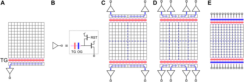
The metal-oxide-semiconductor (MOS) CCD structure consists of polysilicon gates on a gate oxide above a silicon substrate. The most common CCD pixel, as illustrated in Figure 1A, has three separate gates (φ1, φ2,φ3). By manipulating the voltages on the gates, charge can be stored (integrated) or shifted from pixel-to-pixel. The simplest CCD detector, Figure 2A has a 2D array of imaging pixels and a 1D array of pixels used as an output shift register. In operation (1) an image is exposed, (2) the first row is shifted into the output shift register via the Array Transfer Gate (ATG), (3) the output shift register pixels individually shifted out and captured, (4) and the next row is then transferred to the output shift register. In most CCDs, an MOS source-follower is used to drive the signal off the sensor. An Output Transfer Gate (TG), Figure 2B, collects the charge from the output shift register, and pushes it over a barrier potential (OG) onto the gate of the source-follower. The voltage on the gate is then
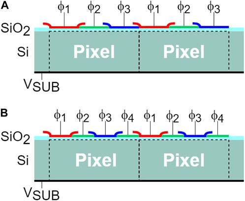
FIGURE 1. 3- and 4-phase CCD pixels. Charge moves left-to-right or right-to-left depending on the sequence of clocks, φ1-4.
To increase the frame rate of the CCD readout, additional parallelism is used. The simplest is reading out from both sides of the CCD: The 4-port CCD (Figure 2C) is a trivial modification of the single port CCD (Figure 2A). Incorporating more output ports becomes more challenging, since the output shift registers must be modified in order to provide the space required for the output stage. Numerous CCDs with more than 4 readout ports (Figure 2D) have been produced: for example, the FastCCD has one port for every 10 columns. The VeryFastCCD is a fully-column-parallel CCD (Figure 2E)—which means that every CCD column has a readout port. Because there is not enough space for an output stage (Figure 2B) for each column, the VeryFastCCD directly outputs a charge rather than a voltage.
The FastCCD and VeryFastCCD are fabricated in the Dalsa 2.5 μm, triple poly, triple metal process1 on very high resistivity n-type silicon with buried p channels, using a method developed at LBNL(2). For CCDs operating at high speed, the long polysilicon gates must be “metal strapped”—that is covered with metal lines, which are ∼1/1000 the resistivity of the polysilicon, and connected as frequently as possible to the polysilicon. For the FastCCD, we chose to use a single metal layer, and designed a 30 μm, 3-phase (Figure 1A) pixel. For the VeryFastCCD, we chose to use 3 metal layers. Since here a charge, rather than voltage, output, is used, parasitic charge injection (through substrate or other capacitive coupling to the output) can present large transients to any downstream amplifier, and potentially saturate the amplifier output. For this reason, we designed a 4-phase (Figure 1B) pixel in order to minimize parasitic charge injection from the CCD clocks since 4-phase clocking provides first order cancellation at each clock transition (
Since the CCDs are generally thick (100s of μm) to have good X-ray absorption, they are “self-shielding” against radiation damage when back-illuminated. Figure 3 shows the cumulative photon flux per pixel to accumulate 1 MRad in the gate oxide for a 200 μm thick sensor (the thickness of the VeryFastCCD). Measurements at DORIS with hard X-rays on the FastCCD indicate that 1 MRad will induce sufficient leakage current to limit performance with 10 ms exposure times. This suggests no radiation damage for soft X-ray storage ring use, nor at FELs (under normal circumstances).
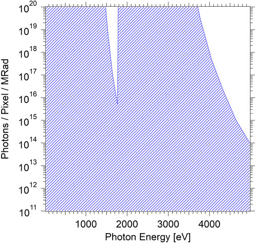
FIGURE 3. Calculated number of photons per VeryFastCCD pixel required to deposit 1 MRad in the CCD gate oxide as a function of energy.
The VeryFastCCD uses all of the same sensor fabrication and processing methods as the FastCCD. A fabricated wafer is shown in Figure 4. Both 256 × 256 pixel and 512 × 512 devices are present. The 512 devices are arrayed in such a way that four of them can be diced to create a 1024 × 1024 sensor with 90% fill factor.
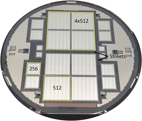
FIGURE 4. A 150 mm VeryFastCCD production wafer, containing 8 256 × 256 and 8 512 × 512 CCDs. Four 512 × 512 CCDs can be diced out as a single 1024 × 1024 CCD.
2.1 Thin entrance windows
High efficiency detection of soft X-rays requires a back side illuminated CCD with minimal dead material between the incident X-ray and the active silicon. To deplete the thick active volume, a voltage must be applied to the back (X-ray entrance) side of the CCD (VSUB in Figure 1). A very thin contact layer is thus required. Soft X-ray detection also requires very low noise, hence the contact must ensure minimal leakage current. While Schottky barrier contacts exhibit a very thin dead layer, they result in leakage currents that are high for soft X-ray applications. An ohmic contact is thus preferred and used here.
The technique initially developed at LBNL for fabricating thick, high resistivity CCDs is to use doped polysilicon to form the thin X-ray entrance contact [6]. However, polysilicon deposition requires temperatures that are too high to be compatible with aluminum metallization. When this technique is used, wafers are (a) implanted and gates formed at the factory (b) thinned and then the doped polysilicon contact is deposited at LBNL (c) final metalization is performed at LBNL. As the LBNL metal process has only one layer, and larger-sized vias than the triple-metal Dalsa process, having a low temperature process that can be performed on fully metallized wafers (a) simplifies the CCD fabrication process since all of the steps except the thin contact fabrication can first be performed at the foundry (b) enables the use of more metal layers, which improves the high-speed CCD clock distribution.
The thin X-ray entrance contact is then added to the device at LBNL as the last processing step. To this end we have developed two low temperature thin contact processes: (1) implantation followed by low temperature annealing (∼100 nm thick), and (2) molecular beam epitaxy (MBE) (∼10 nm thick). The MBE contact has the added benefit of being even thinner than the doped polysilicon contact (∼30 nm thick).
The ion implanted contact generally finds use for applications in which the energies of the incident photons are 500 eV or more. This contact has the advantage of being relatively simple to fabricate. The MBE contact is used to extend the reach to lower energies.
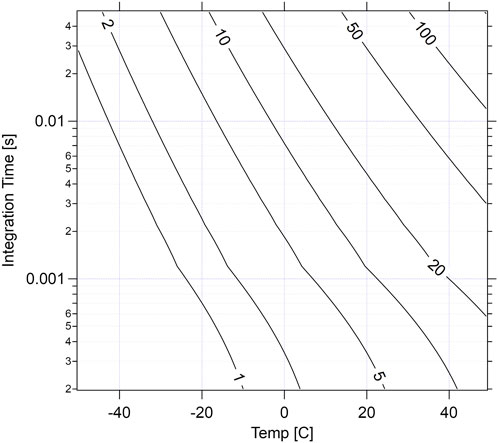
We have evaluated the quantum efficiency (QE) of both of these types of contacts on numerous samples (CCDs and diodes) using the metrology beamline2 (6.3.2) at the Advanced Light Source [7]. Figure 5 shows the averages of QE measurements for the two types of contacts. Figure 6 shows the leakage current for the 10 nm contact on a 256 × 256 VFCCD as a function of temperature, T. The temperature dependence of the leakage current is modeled [8, 9] as
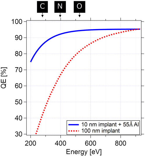
FIGURE 5. Quantum Efficiency for 10 and 100 nm contacts measured at ALS Beamline 6.3.2. Shown are fits of the measurements. Energies of the carbon, nitrogen and oxygen K-edges are highlighted.
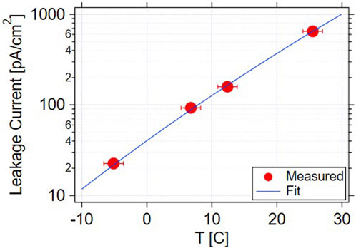
FIGURE 6. Leakage current for 200 μm thick CCD with 10 nm contact as a function of temperature. The points are measured values, and the curve is a fit as described in the text.
While the VeryFastCCD has a high frame rate, different experimental conditions necessitate different exposure times. A key system design parameter is the camera operating temperature, and this is determined by the noise added by leakage current: that added noise is proportional to
3 Data acquisition
Data acquisition is illustrated in Figure 8. The CCD signal is read out on two sides (Figure 2E), and the other two sides are used to provide clocks. A 256-channel integrated circuit VASE2 has been developed to read out the charge from the VeryFastCCD. (A prior version VASE1 is described in [10] and was subsequently simplified for VASE2 by removing a ΣΔ gain stage.). One VASE2 handles 256 CCD channels. Each CCD output is wire-bonded to a VASE2 input. Internally, VASE2 consists of 16 modules: each module has 16 front-end circuits and a 16:1 analog multiplexer. Each 8 of the VASE2 outputs are input to a commercial 8-channel, 16-bit ADC (TI ADS52J65). High-speed outputs from the ADCs are converted to optical signals, driven off the camera via fiber-optic ribbons.
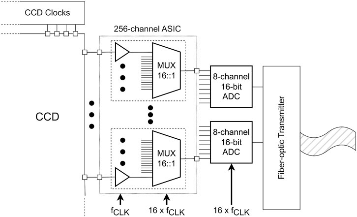
FIGURE 8. VeryFastCCD system overview: 256 CCD outputs are processed by a single VASE ASIC, whose outputs are digitized by 16 ADCs. Output data are transmitted over fiber optic ribbons.
For a 256 × 256 pixel camera, 2 VASE2 and 4 ADCs are used; for a 512 × 512 camera, 4 VASE2 and 8 ADCs are used, and this doubles again for a 1024 × 1024 camera.
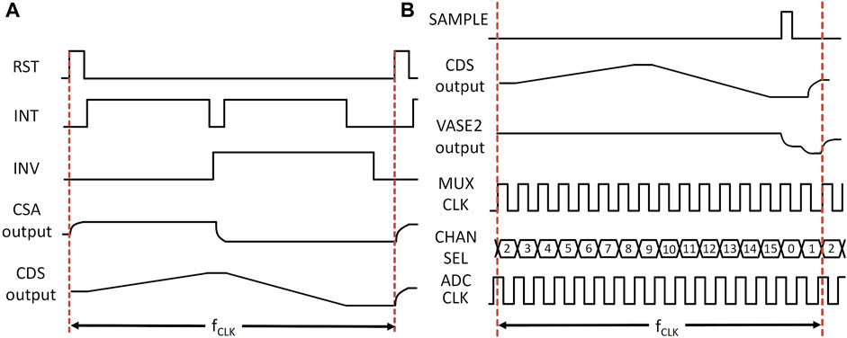
A single VASE2 front end is shown in Figure 9. Similar to the FastCCD [11], the CCD signal is voltage-integrated, with a programmable gain and analog inversion to allow correlated double sampling (CDS). Unlike conventional CCDs, the VeryFastCCD signal is charge: VASE2 thus incorporates a charge-sensitive amplifier (CSA) with reset. As shown in Figure 10A, the RST switches are closed, removing charge on capacitors CF and CINT. The RST switches are then opened and switch INT is closed for time TINT, and the reset level (VRST) is integrated on capacitors CINT. Switch INT is then opened, and CCD charge is presented to the CSA. The CSA output is
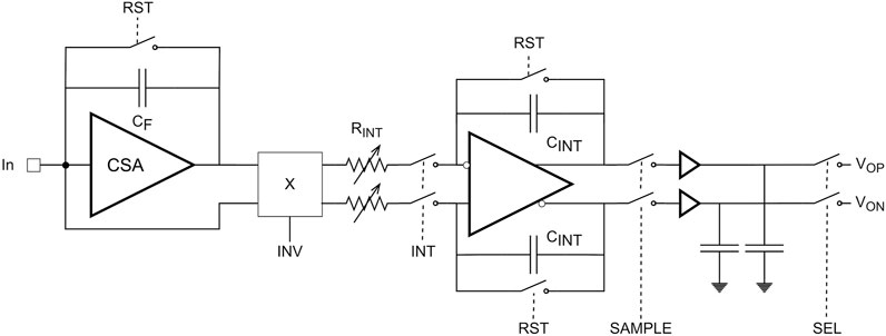
FIGURE 9. VASE2 Front end, with charge-sensitive amplifier, programmable integrator and output sample/hold.
The CCD row clocks and the VASE2 front end clocks (shown in Figure 10A) both operate at frequency fCLK. The VASE2 back end and ADC operates at 16xfCLK. As illustrated in Figure 10B, each front end stores the value of VINT for CCD row N on a sample-and-hold circuit when the SAMPLE command is issued. While the front end proceeds to acquire the signal from CCD row N+1, the 16 stored values for row N are multiplexed and digitized.
All of the measurements described below were performed with 256 × 256 CCD cameras. All of the CCDs were 200 μm thick, and operated at reverse bias of up to 80V. Several versions, equipped with HG and LG VASE2 chips, along with both 10 nm and 100 nm contacts have been tested. Cameras were also tested at the COSMIC beamline3 at ALS [12], and the SXR beamline at LCLS I. The cameras were operated at fCLK = 1.28 MHz, corresponding to up to 10,000 frames/s (equivalently 5,000 frames/s for a 512 × 512 device).
A timing diagram is shown in Figure 11. Clocks to the VASE2s and ADCs are continuous. CCD clocks also operate at fCLK = 1.28 MHz. For storage ring applications, with signal integration times

FIGURE 11. CCD and VASE front end timing: VASE clocks run continuously whereas CCD clocks are paused during signal integration. The colored circles represent pixel signals–as they are shifted by the CCD clocks and finally captured by the VASE SAMPLE signal.
4 Results
The digitized signal value is
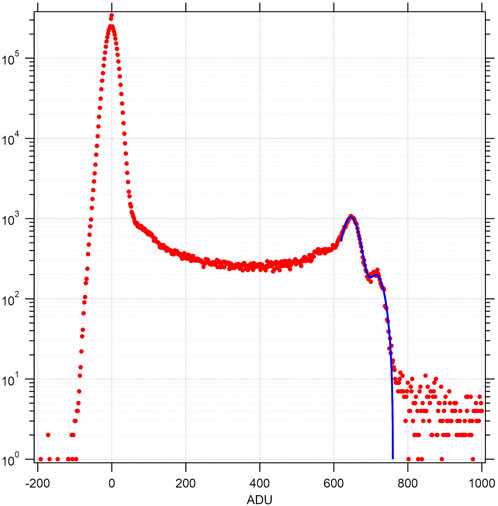
FIGURE 12. Spectrum (red) from all pixels illuminated by a 55Fe source. The blue curve shows a fit to the combined Kα/Kβ lines.
Figure 13A shows the maximum photon energy deposited in a pixel that can be recorded (before the ADC saturates) vs. the ENC for different gain settings of the high gain version of VASE2. Figure 13B shows the values for the low gain version of VASE2. On a given gain range, the full-scale divided by the noise is 10–12 bits (larger as the gain is reduced).
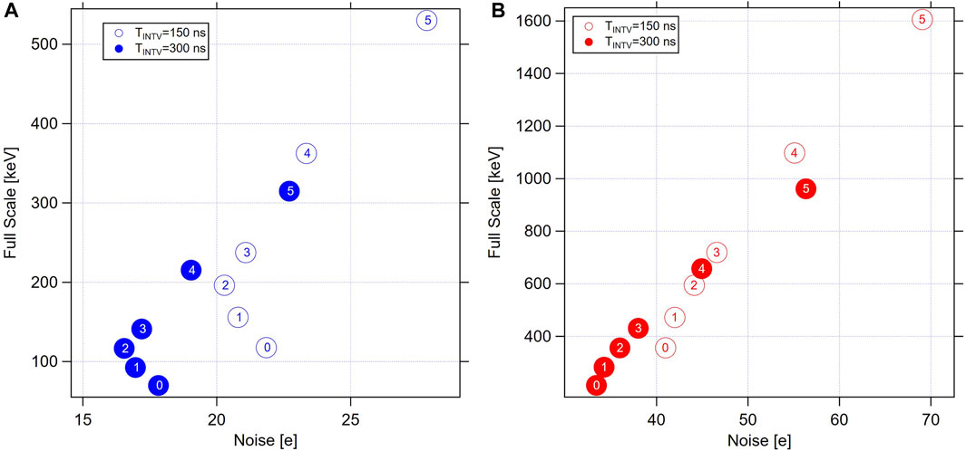
FIGURE 13. Maximum photon energy per pixel that can be recorded vs. Equivalent Noise Charge (ENC) for (A) VASE2 HG (B) VASE2 LG. The numbers in the circles are the gain setting, with 0 being the highest gain and 5 being the lowest. For both (A,B) values are shown for the nominal
The digitized noise is
As described above, the VASE signal is proportional to integration time. By reducing the integration time, a larger full scale signal can be accommodated on a given gain range. Figure 14A shows the roughly linear reduction in signal with integration time. Of course, decreasing the integration time increases the noise bandwidth by
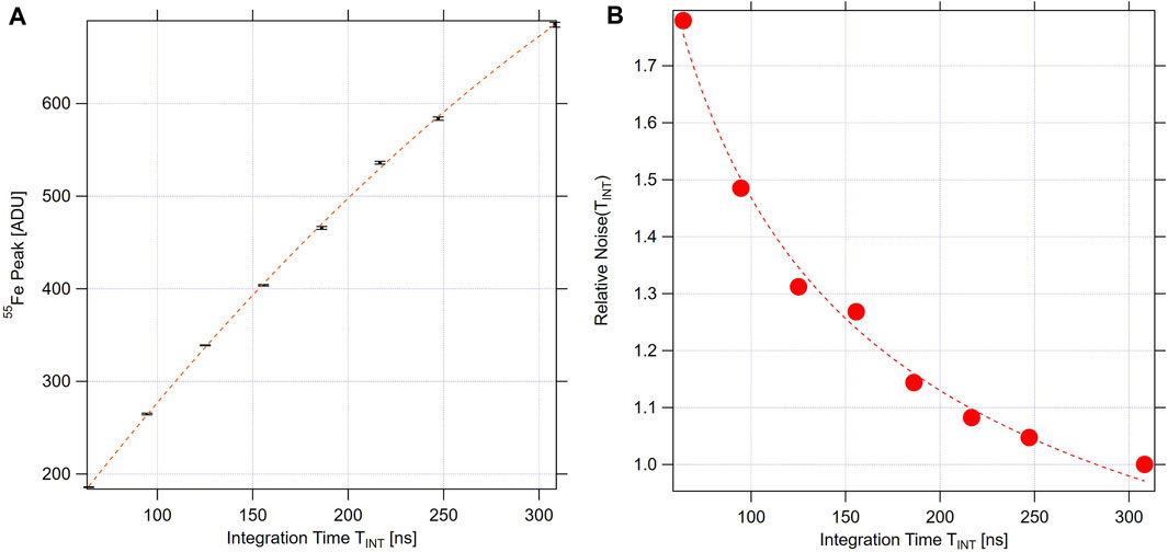
FIGURE 14. (A) 55Fe peak position as a function of integration time. The curve is a quadratic fit. (B) Noise relative to nominal integration time of 305 ns. The curve is a fit to
5 Conclusion
The VeryFastCCD is the fully-column-parallel successor to the FastCCD. Fabricated in the same CCD process, it has a 25 times higher frame rate. With 10 nm and 100 nm entrance window contacts, it has high quantum efficiency for soft and tender X-rays. The custom readout circuit has programmable gains and can also use integration time as a way to trade full-scale signal for noise. Prototype versions have been tested at ALS and LCLS, and systems for ALS are currently being prepared.
Data availability statement
The raw data supporting the conclusion of this article will be made available by the authors, without undue reservation.
Author contributions
AG: Formal Analysis, Writing–review and editing. CG: Conceptualization, Methodology, Writing–review and editing. JJ: Methodology, Writing–review and editing. AK: Methodology, Writing–review and editing. CT: Methodology, Writing–review and editing. PD: Conceptualization, Methodology, Project administration, Writing–original draft.
Funding
The author(s) declare financial support was received for the research, authorship, and/or publication of this article. This work was funded by the U.S. Department of Energy, Office of Basic Energy Sciences, Scientific User Facilities Division, through grants from the Accelerator and Detector Research Program, and by the Linac Coherent Light Source and the Advanced Light Source. Work was performed at the Lawrence Berkeley National Laboratory, which is supported by the U.S. Department of Energy under contract no. DE-AC02-05CH11231.
Acknowledgments
The authors would like to acknowledge members of the LBNL Engineering Division: Ian Johnson, Thorsten Stezelberger and Vamsi Vytla for design and development of the data acquisition system, and Armin Karcher for electronics design. We also acknowledge design concepts and measurement support from Rebecca Armenta, Gabriella Carini, Philip Hart, Mark McKelvey, and Kaz Nakahara of the Linac Coherent Light Source and Rich Celestre and David Shapiro of the Advanced Light Source.
Conflict of interest
The authors declare that the research was conducted in the absence of any commercial or financial relationships that could be construed as a potential conflict of interest.
Publisher’s note
All claims expressed in this article are solely those of the authors and do not necessarily represent those of their affiliated organizations, or those of the publisher, the editors and the reviewers. Any product that may be evaluated in this article, or claim that may be made by its manufacturer, is not guaranteed or endorsed by the publisher.
Footnotes
1https://www.teledynedalsa.com/en/products/foundry/ccd/
3https://als.lbl.gov/beamlines/7-0-1-2/
4https://www.ti.com › dataconverters › ads52j65.
References
1. Boyle WS, Smith GE. Charge coupled semiconductor devices. Bell Syst Tech J (1970) 49(4):587–93. doi:10.1002/j.1538-7305.1970.tb01790.x
2. Stover RJ, Wei M, Lee Y, Gilmore DK, Holland SE, Yi X, et al. High-performance CCD on high-resistivity silicon. In: Imaging System Technology for Remote Sensing: Proceedings of SPIE (1998). p. 13–8.
3. Struder L, Brauninger H, Briel U, Hartmann R, Hartner G, Hauff D, et al. A 36 cm2 large monolythic pn-charge coupled device x-ray detector for the European XMM satellite mission. Rev Scientific Instr (1997) 68(11):4271–4. doi:10.1063/1.1148341
4. Denes P, Doering D, Padmore HA, Walder JP, Weizeorick J. A fast, direct x-ray detection charge-coupled device. Rev Scientific Instr (2009) 80(8):083302. doi:10.1063/1.3187222
5. Kameshima T, Ono S, Kudo T, Ozaki K, Kirihara Y, Kobayashi K, et al. Development of an X-ray pixel detector with multi-port charge-coupled device for X-ray free-electron laser experiments. Rev Scientific Instr (2014) 85(3):033110. doi:10.1063/1.4867668
6. Holland SE, Wang NW, Moses WW. Development of low noise, back-side illuminated silicon photodiode arrays. IEEE Trans Nucl Sci (1997) 44(3):443–7. doi:10.1109/23.603687
7. Underwood JH, Gullikson EM, Koike M, Batson PJ, Denham PE, Franck KD, et al. Calibration and standards beamline 6.3.2 at the advanced light source. Rev Scientific Instr (1996) 67(9):3372. doi:10.1063/1.1147338
8. Sze SM, Ng K. p-n Junctions. In: Physics of semiconductor devices. New Jersey, United States: Wiley (2006). p. 77–133.
9. Chilingarov A. Temperature dependence of the current generated in Si bulk. J Instrumentation (2013) 8(10):P10003. doi:10.1088/1748-0221/8/10/p10003
10. Grace CR, Denes P, Fong E, Goldschmidt A, Papadopoulou A. A 4-MHz, 256-channel readout ASIC for column-parallel CCDs with 78.7-dB dynamic range. IEEE Trans Nucl Sci (2020) 67(5):823–31. doi:10.1109/tns.2020.2980769
11. Walder JP, Denes P, Grace C, Hvd L, Zheng B. A fast low noise CMOS charge sensitive preamplifier for column parallel CCD readout. In: 2011 IEEE Nuclear Science Symposium Conference Record; 30 October - 6 November 2010; Knoxville, Tennessee, USA (2011). p. 721–4.
Keywords: soft X-ray detector, direct-detection CCD, readout ASIC, thin contacts, sensors
Citation: Goldschmidt A, Grace C, Joseph J, Krieger A, Tindall C and Denes P (2023) VeryFastCCD: a high frame rate soft X-ray detector. Front. Phys. 11:1285350. doi: 10.3389/fphy.2023.1285350
Received: 29 August 2023; Accepted: 16 October 2023;
Published: 26 October 2023.
Edited by:
Jiaguo Zhang, Paul Scherrer Institut (PSI), SwitzerlandReviewed by:
Gabriele Giacomini, Brookhaven National Laboratory (DOE), United StatesKonstantin Stefanov, The Open University, United Kingdom
Robert Andritschke, Max Planck Institute for Extraterrestrial Physics, Germany
Copyright © 2023 Goldschmidt, Grace, Joseph, Krieger, Tindall and Denes. This is an open-access article distributed under the terms of the Creative Commons Attribution License (CC BY). The use, distribution or reproduction in other forums is permitted, provided the original author(s) and the copyright owner(s) are credited and that the original publication in this journal is cited, in accordance with accepted academic practice. No use, distribution or reproduction is permitted which does not comply with these terms.
*Correspondence: Peter Denes, cGRlbmVzQGxibC5nb3Y=
 Azriel Goldschmidt
 Carl Grace
 John Joseph1
 Amanda Krieger
 Peter Denes