
94% of researchers rate our articles as excellent or good
Learn more about the work of our research integrity team to safeguard the quality of each article we publish.
Find out more
ORIGINAL RESEARCH article
Front. Phys., 07 July 2023
Sec. Optics and Photonics
Volume 11 - 2023 | https://doi.org/10.3389/fphy.2023.1170265
This article is part of the Research TopicTerahertz Optics and DevicesView all 15 articles
 Yuhui Zhang1*
 Michael Shur1,2*
We show that a periodic multi-grated-gate structure can be applied to THz plasmonic FETs (TeraFETs) to improve the THz detection sensitivity. The introduction of spatial non-uniformity by separated gate sections creates regions with distinct carrier concentrations and velocities, giving rise to harmonic behaviors. The resulting frequency spectrum of DC voltage response is composed of “enhanced” and “suppressed” regions. In the enhanced region, the amplitude of response voltage can be enlarged up to ∼100% compared to that in a uniform channel device. The distribution pattern of those regions is directly related to the number of gate sections (Ns). A mapping of response amplitude in a Ns-frequency scale is created, which helps distinguish enhanced/suppressed regions and locate optimal operating parameters.
Short channel field-effect transistor (FET) operated in plasmonic regime at sub-THz or THz frequencies (often referred to as TeraFETs [1, 2]), are promising devices for THz applications such as sensing [3–7], imaging [8–10], and beyond-5G communication [1, 3]. TeraFETs can work in the plasmonic resonant (ballistic or viscous) regimes [11, 12], in which the plasma waves are generated [13, 14]. Such hydrodynamic-like property allows TeraFETs to break the frequency limitation set for collision-dominated devices and operate at GHz to THz ranges. TeraFETs are also tunable by the gate bias or doping or illumination [15–17], The high speed of plasma waves enables TeraFETs to be a strong candidate for ultrashort pulse detection [18, 19].
To facilitate the industrial applications of TeraFETs, one of the key issues is to improve the detection sensitivity. As was discussed in [1], further improvement in the noise-equivalent power of TeraFETs is required to enable 6G communication applications. A straightforward way is to use better materials, e.g., materials with high mobility (μ) and high effective mass (m*), so as to elevate the device quality factor (Q = ωpτ, where ωp is the plasma frequency, τ = μm*/e is the momentum relaxation time) [20]. We have demonstrated that p-diamond could be a valid candidate for high-sensitivity THz and sub-THz detections [21–23]. In addition to the material consideration, one can also resort to new structural designs. The non-uniform structures, such as grating gates [24–28], dense arrays [29–31], and plasmonic crystals [24, 32], were introduced and proved to be effective in improving the TeraFET detection performance.
The introduction of specifically-arranged non-uniform structures in TeraFETs can modify the carrier density, static field distribution, and plasma wave velocity along the device channel, thus altering the THz rectification properties and/or the wave propagation features. For example, with a split-gate structure and a graded doping (i.e., the grating-gate), the circularly polarized THz radiation can be rectified by the TeraFET, inducing DC currents in both parallel and transverse directions [16, 28]. It was shown that the DC current flux in the transverse direction is related to the helicity of the THz radiation, and this current is dramatically enhanced near the plasmon resonant frequencies. The multi-gates can also be rearranged to create a concatenated FETs dense array, where the source, drain, and gate are all split into fingers and nested together to form the repeated unit cells [30, 31, 33]. Such short-period grating of metal contacts strengthens the device asymmetry and serves as an effective antenna coupling incident THz radiations, thereby improving the detection sensitivity. In addition, the grating-gate structure can also synergize with the applied DC current to create full transparency and the amplification of THz radiation [34].
In our recent work [2], we used a spatially non-uniform gate capacitance or threshold voltage to induce the channel nonuniformity. Those structures are capable of modifying the transport properties of plasma waves and enhance or suppress the non-resonant photoresponse [2, 35]. However, those structures contained spatially nonuniform dielectric layer and coordinate-dependent doping, making the device fabrication costly and cumbersome in real-world applications. Inspired by the periodic gate structures in previous works, in this work, we bring periodic multi-gate structures to our TeraFETs, and explore the effects of these structures on the resonant THz detection performance in a wide spectral range, including harmonic plasmonic modes. Compared to the varying capacitance or varying threshold voltage designs, the periodic gate structure is easier to fabricate as it does not require dielectric profiling or coordinate-dependent doping. As will be shown later, the periodic multi-gate TeraFETs possess strong harmonic behaviors and can reach a ∼100% improvement in DC voltage response near the resonant peaks. The demonstrated improvement is achieved without a DC current bias, and thus it does not rely on any DC field effect or plasmonic instability mechanism.
In addition to the internal TeraFET responsivity, the measured responsivity depends on the THz-antenna coupling efficiency [36, 37] and the impedance matching [38]. The antenna coupling efficiency signifies the ratio of antenna collected power to the THz radiation power, and is related to the design of antenna [36] or the arrangement of dense gate arrays [29]. In this work, we only focus on the device-level improvement of THz detection sensitivity. Our results allow optimizing the TeraFET parameters per unit width, since we consider a one-dimensional model. We consider using a periodic multi-gate TeraFET structure to achieve high-sensitivity resonant THz detection. Figure 1A shows the schematic of the structure. The gates are driven by periodic-in-space DC excitations. The number of gate sections (Ns) is adjustable. In a system design, we could match the TeraFET impedance to the antenna impedance and to the load impedance by choosing the number of gate fingers and optimizing the gate finger dimension. With the repetitive excitation of DC biases Vg1 and Vg2, the spatial distribution of DC gate voltage can be approximated by a square-wave voltage shown in Figure 1B. Here Ns is the number of split gates, PL and PH are the duty ratios of high and low voltage in one high-low cycle, respectively. PC is the ratio of one high-low cycle in the whole channel. Nc is the number of complete high-low cycles. We define PL + PH = 1, (NC + PL)PC = (NC+1-PH)PC = 1. Besides, α is a voltage modulation factor, Vg0 is a reference gate voltage. The square-wave approximation can be verified via electrostatic modeling (see Supplementary Material S1). A more realistic consideration is to include the transition regions between each two adjacent sections, as illustrated by dashed lines in Figure 1B. The transition region here results from the separation (i.e., the ungated region) between two adjacent gate segments. We assume that the length of the separated region is short so that carriers underneath can be screened by the peripheral voltage of neighboring gates. Therefore, we still consider the transition regions as gated regions.
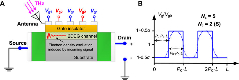
FIGURE 1. (A) Schematic of THz detection by a periodic multi-gate TeraFET. (B) The resulting spatial distribution of DC gate bias. The ideal and realistic distribution curves are illustrated in solid and dashed lines, respectively.
We use a 1D hydrodynamic model [12, 15, 39] to simulate the response of the proposed TeraFET structure. The detailed introduction and validation of the model can be found in [12]. The key equations are:
where n, u are the carrier density and hydrodynamic velocity, respectively. m* is the effective mass of carriers. U is the gate-to-channel voltage defined as U(x) = U0(x)—Uch(x), where U0(x) = Vg(x)—Vth(x) is the gate bias beyond threshold, Uch(x) is the channel potential. In order to ensure that the device works in hydrodynamic regime, the scattering rates should satisfy γee > max[γe-ph, γe-imp] [40], where γee, γe-ph, and γe-imp are the electron–electron, electron–phonon, and electron–impurity scattering rates, respectively. With a relatively low mobility set in our device (0.1 m2/Vs), this condition can be met in the low bias region [21].
A unified charge-control model [41, 42] is used to related n and U:
where Vt = kBT/e is the thermal voltage (kB: Boltzmann constant, T: temperature, fixed at 300 K). η is an ideality factor. The UCCM is valid as long as 1) the capacitive coupling between the gate and the device channel is valid and 2) the leakage current through the intrinsic capacitances (for example, the gate-to-source capacitance Cgs) is not too large as compared to the channel current. We have checked that those conditions can be met for TeraFETs considered in this work (see Supplementary Material S1 for details).
In this work, we focus on the effects of non-uniform Vg on the detection performance of TeraFETs in absence of any helicity-sensitive effects. For multiple-gate TeraFETs, the so-called ratchet effect could lead to the plasmonic enhanced rectification [28]. In this paper, we consider TearFETs with the variable gate voltage swing, where the ratchet effect is not important. We consider a multi-gate whose gate section near the source is connected with a THz coupling antenna, as shown in Figure 1A. In this way, the device absorbs the THz radiation only by the leftmost gate section, and consequently the boundary condition at the source can be approximated by U(0,t) = U0(0) + Ua(0,t) [20], where Ua(0,t) = Vam·cos(ωt) represents the AC small-signal voltage induced by the incoming THz radiation. We set Vam to 2 mV, which can be treated as a small signal with respect to the bias. On the drain side, an open circuit condition is used, i.e., J(L, t) = 0, where J is the current flux density, L is the channel length. With the above design, the plasma waves can be generated near the source side and get rectified by periodic gate biases while propagating along the channel. The DC response voltage can then be obtained by measuring the drain voltage and extracting its DC component.
In addition to the plasmon-induced response, there are other THz rectification mechanisms in TeraFETs, such as photo-thermoelectric effect [43] and junction linearity in tunneling FETs [44], quantum wells [45]. Similar effects has also been observed in HBTs [46]. In this work, we focus on the hydrodynamic nonlinearity enhanced by plasmons. We investigate split-gate Si MOSFET biased at a relatively low voltage at room temperature.
Based on the above model settings, we simulate our device and evaluate the frequency spectrum of DC source-to-drain response voltage (dU). According to Dyakonov-Shur theory [20], dU is proportional to the intensity of THz signal, which, in turn, is proportional to the squared THz voltage amplitude. For a single-gate device, the response has the form [20].
where ω is the angular driving frequency, f(ω) is a frequency-dependent function associated with the plasma wave (or damped electron wave) propagation properties. Generally, Eq. 4 applied to uniform-channel devices (i.e., single gate and no drain bias). Our recent work have shown that (4) can also be modified to evaluate the response in spatially nonuniform channel TeraFETs, such as exponentially-varying gate capacitance devices [2] and current-driven TeraFETs [47]. Besides, (4) does not take into account the device loading effect and thus only applies to devices with an infinite load impedance (e.g., an open-drain TeraFET). With a finite load resistance RL, the output response voltage dUo can be expressed by dUo = dUI/(1+ Rch/RL) [48, 49], where dUI is the intrinsic response given by (4), and Rch is the channel resistance. Due to the voltage divider effect, the loaded TeraFET has a lower response voltage compared to the unloaded ones under the same operating conditions.
The results under linear Vg(x) profile and 3 different Ns values under multi-gate structure are presented in Figure 2. These results are for a Si FET with 50% duty ratio (PL = PH = 50%, see Figure 1), and Vg0 = −0.2 V, Vth = 0.2 V, Vam = 2 mV, and at room temperature. Now the fundamental resonant frequency f0 is at 0.515 THz, and the device is driven into the subthreshold mode with a low electron density (∼1014 m-2) but a relatively large voltage response [49, 50]. To improve convergence, the continuous-first-derivative transition regions are set between neighboring gate sections, and the relatively size of those regions (Tz, the ratio of total transition region size over the whole channel size) is fixed at Tz = 0.1 (see more details in Supplementary Material S1). The number of sections varied from 2 to 7. The voltage applied to different gates varied (see Figure 1B). Table 1 lists the major parameters used in the simulation.
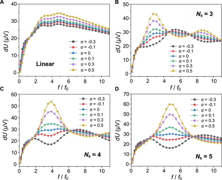
FIGURE 2. DC response voltage (dU) as a function of frequency (f) in a Si TeraFET with different channel designs. (A) Linearly distributed gate voltage. (B) Periodic multi-gate with Ns = 3. (C) Periodic multi-gate with Ns = 4. (D) Periodic multi-gate with Ns = 5.
TABLE 1. Simulation parameters used in this work.
Figure 2A shows the result under a linear varying gate voltage: Vg(x) = Vg0(1+α(x-0.5L)/L). We can see that with the increase of α (or the decrease of DC gate bias swing from source to drain since Vg0 is negative), dU decreases when f < f0, where f0 = S/4L is the fundamental resonant frequency, S is the plasma wave velocity [22, 50]. This region corresponds to the non-resonant operation region of the device. Using the methods in [2, 50], we can get the expression of DC response in this region (see Supplementary Material S1 for detailed derivations):
where β = 1/sqrt(1+(ωτ)−2), k1, k2 are wave vectors of the plasma wave:
Here
Figure 2B shows the result of dU vs α under Ns = 3. Compared to Figure 2A, the 3-segment multi-gate TeraFET exhibits a distinct response profile, and Eq. 6 fails in this case. As f rises, the response voltage oscillates, and the variation trend of dU with respect to α changes multiple times. If we define the regions where dU increases with rising α as the “enhanced” regions, and the regions where dU decreases with rising α as the “suppressed” regions, we can see that the enhanced and the suppressed regions appear alternatively with the increase of frequency. More interestingly, the positions of those regions are directly related to the number of gate sections. For example, the peak response voltage in the first enhanced region (which is also the peak dU in the whole frequency range) is at f = 3f0, the position of response valley in the first suppressed region is f = 6f0, and the position of peak response in the second enhanced region is at f = 9f0. Thus, we conclude that the frequency at which the maximum response is reached is around
and the frequency gap between two adjacent peaks or valleys is
Eqs 8, 9 indicate that we can selectively enhance the resonant detection responsivity in a given frequency band by properly selecting the number and length of gate sections in a TeraFET. This result is similar to those reported in [34, 51], where the THz transmission spectra was controlled by the gate separations in grating-gating graphene FETs, and the resonant frequency was determined by the unit finger gate width (∼L/Ns). However, unlike the current-driven boundary condition used in [34, 51], here we used an open-drain condition. Thus the enhancement and suppression of voltage response are independent of plasmonic instability or DC field effects, and solely originate from the setup of plasmonic cavities. Besides, the TeraFETs used in this work operate in the subthreshold region, in which the electron density and plasma wave velocity are less sensitive to the gate bias variations [50]. This helps stabilize the resonant frequency at each order (since f0 = S/4L, where f0 is the fundamental resonant frequency). This explains why there is no significant redshift or blueshift observed in Figure 2 as α changes.
Eqs 8, 9 can be further verified by the simulations under other Ns values. For example, in Figure 2C where Ns = 4, the peak frequency is at 4f0 and the distance between two adjacent peaks or two adjacent valleys are 8f0. In Figure 2D where Ns = 5, the values of fp and dfp are 5f0 and 10f0, respectively. Also, a 100% increase in dU (compared to the uniform channel case) is achieved when α reaches 0.5. Note that the peaks and valleys are not located at the fundamental resonant frequency, but at the higher order harmonics. Therefore, the introduction of multiple gate sections activated the harmonic components in the system, resulting in the distribution of enhanced and suppressed regions. The underlying mechanism could be related to the reflection of plasma waves or carrier drift between neighboring sections due to the carrier concentration barriers. Those reflections change the wave propagation properties (i.e., k1 and k2) and shorten the effective channel length, thereby leading to the excitation of harmonic peaks and valleys. Figure 3A shows the spatial distribution of gate-induced field (dVg/dx) along the channel. The abrupt change of DC gate bias in the narrow transition regions creates a large field on the order of 0.1 MV/cm. The electrons passing the transition regions get accelerated or de-accelerated, forming the separated velocity distribution regions, as demonstrated by the velocity distribution contour plot in Figure 3B. Each curve in Figure 3B represents the carrier velocity distribution u(x) at a given moment in one AC period, and 50 consecutive moments are included. The separated velocity distribution regions could induce the reflections of plasma waves in between, thereby altering the DC response properties.
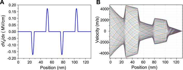
FIGURE 3. Spatial distributions of (A) the gradient of DC gate bias (dVg/dx) and (B) variation contour of carrier velocity at α = 0.3. Other parameters follow those in Figure 2.
The above harmonic excitation mechanism can be seen as a result of abrupt changes in channel properties, as opposed to the gradual changes reported in our previous work [2]. In a gradually varying channel, the response performance is related to the changing rate of channel parameters (e.g., the gate capacitance, threshold voltage, DC gate bias). While in multi-gate setup, we can verify from simulation that the response dU is insensitive to the transition region size Tz (see supplementary material). This indicates that the response profile is now level-sensitive, as opposed to the gradient-sensitive ones in [2]. Therefore, the analytical approaches developed in [2] can no longer be applied here.
To further investigate the variation trend of dU with frequency, we define a differential response voltage ddU = dU(α = 0.3) - dU(α = 0), and plot its frequency profile at different Ns values, as shown in Figure 4. Here ddU signifies the net enhancement or suppression of dU at α = 0.3 as compared to the uniform channel case. In Figure 4A, the amplitude of ddU rises with the increase of Ns. This suggests that the enhancement effect strengthens as the channel becomes more non-uniform. With the rise of frequency, ddU oscillates and exhibits multiple peaks and valleys, as shown in the separated plots Figures 4B–D. For quantitative analysis, we plot Figure 5 where ddUmax, fp and dfp as functions of Ns are presented. One can check that the fp and dfp curves follow Eqs 8, 9. The ddUmax increases with the rise of Ns, but a saturation trend is observed when Ns becomes large. This saturation could be related to the change of wave reflection characteristics as the length of each gate section shortens, which sets a limit to the maximum improvement of dU.
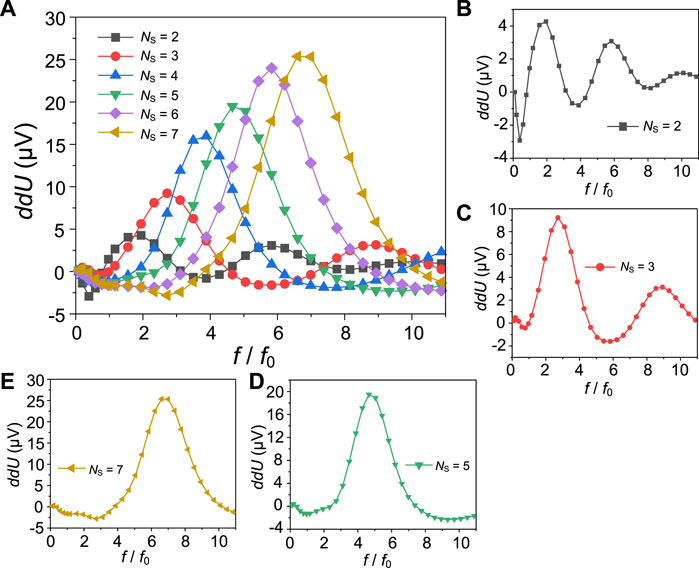
FIGURE 4. (A) ddU as a function of f/f0 for Ns = 2∼7 and (B–E) separated plots with Ns = 2, 3, 5, and 7, respectively. Other parameters follow those in Figure 2.
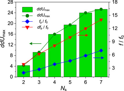
FIGURE 5. The peak value of ddU (ddUmax, in μV), the frequency at which ddU reaches the maximum (fp), and the frequency gap between two adjacent peaks or valleys (dfp) as functions of Ns.
To better understand how the response changes with frequency and gate structure, we create a map of ddU in a Ns-f/f0 scale, as shown in Figure 6. In the map, the enhanced regions are exhibited as “mountains” while the suppressed regions are presented as “valleys”—a result of the present ddU definition. The highest mountain group is located at f = Nsf0, as shown in Figure 6A, which corresponds to the maximum (the first) resonant peak in each case. The second mountain series are at f = 3Nsf0, demonstrating the secondary resonant peaks. Between these two mountain groups is a valley group located at f = 2Nsf0. In general, the mountain clusters can be expressed by f = (2n+1)Nsf0, where n = 0,1,2 … , and the valley clusters follow f = (2n+2)Nsf0.
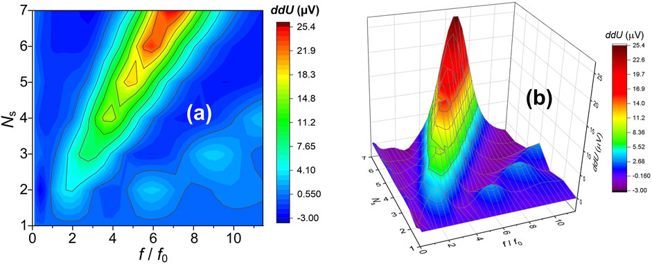
FIGURE 6. 2D mappings of ddU in a Ns-f/f0 scale. (A) 2D contour plot, (B) 3D colormap surface plot. The data presented are the same as those in Figure 5.
Figure 6B shows the direct comparison of the heights of different mountains (i.e., the amplitudes of response peaks). Clearly, the mountain height in each group increases with the increase of Ns, and the average/maximum height in the first mountain group is much larger than that in the second mountain group. Thus, to achieve a high response, the TeraFET should operate in the first mountain group, and in general a large gate section number is preferred.
The results in Section 3.1 and Section 3.2 demonstrate that adopting periodic multi-gate structure in TeraFETs can effectively alter the DC voltage response and achieve over ∼100% improvement in dU at certain frequencies. The amplitude of dU can be tuned by Ns and α. In general, a larger Ns or α leads to a higher responsivity in the enhanced region, but the values of Ns or α cannot grow infinitely due to several built-in limits. Here we discuss those limits.
1) Breakdown voltage (vertical). To prevent the breakdown of the barrier material, the following is required
For example, if Eb = 3 V/nm, db = 4 nm, |Vg0| = 0.2 V, we get α < 46.
2) Breakdown voltage (transverse). Let D denotes the transition region length between two gate sections, and D is related to Tz. To prevent dielectric breakdown in the transition region, we need
If Eb = 3 V/nm, |Vg0| = 0.2 V, D = 2 nm, we get α < 30.
3) Conductivity limit. When the gate bias decreases in the subthreshold region, the carrier concentration can reduce to very low, so as to choke the current conduction. Assume that the minimum conductivity required for sustaining current conduction is σcr = eμncr, where ncr is the critical carrier density. Using Eq. 3, we get:
If ncr = 1013 m-2, Vg0 = −0.2 V, Vt = 0.026 V (T = 300 K), η = 4, we get |α| < 1.29.
4) Process limit. The fabrication lab conditions determine the maximum number of separated gates that can be built in a TeraFET. If the minimum achievable size is Lmin, then we get Ns-max = [L/Lmin], where [k] denotes the nearest integer that does not exceed k. For example, with L = 250 nm, Lmin = 65 nm, we get Ns-max = 3.
The above conditions, along with other more delicate mechanisms (e.g., the self-capacitance and the built-in voltage between two adjacent gate sections), set limit to the tuning of dU in periodic multi-gate TeraFETs. Despite all those constraints, an ∼100% improvement can still be achieved near the maximum resonant peak, as demonstrated in Figure 2D.
Table 2 summarizes the THz detection performance of TeraFETs with non-uniform gate capacitances and periodic multi-gate structures. The data in this table are taken either from [2] or from this paper. It can be seen that using gate capacitance profiling, the maximum reported response improvement was around 20%. With periodic multi-gate design, the response improvement can rise beyond 100% if sufficient gate sections are introduced. This further exhibits the advantage of periodic multi-gate design over gate capacitance profiling.
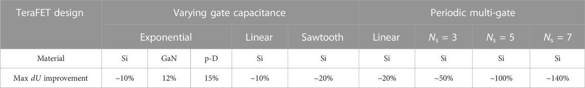
TABLE 2. Comparison of maximum response improvement in different TeraFET designs.
When a periodic multi-gate structure is applied in TeraFETs, the resonant THz detection performance can be improved. The hydrodynamic simulation showed that in periodic multi-gate TeraFETs, the harmonic response peaks were excited, and thus the DC response voltage dU near the harmonic frequencies could increase (“enhanced”) or decrease (“suppressed”) compared to dU in the uniform-channel TeraFETs. The excitation of harmonics peaks could be related to the strong gate-induced field in the transition regions, which accelerates or de-accelerates the carriers and possibly leads to the reflection of plasma waves on the boundaries of gate sections. The frequency spectrum of dU was separated by the “enhanced” and “suppressed” regions, and the distribution of those regions was related to the number of gate splits. The maximum improvement on dU reached beyond 100%. The tunability of dU via gate parameters is limited by the breakdown voltage, conductivity, fabrication resolution, and other more delicate effects. A mapping of variation in dU helps distinguish enhanced/suppressed regions and locate optimal operating parameters.
The raw data supporting the conclusion of this article will be made available by the authors, without undue reservation.
YZ was primarily responsible for the design and realization of numerical simulations. MS supervised the entire work and provided guidance on the theoretical works. All authors contributed to the article and approved the submitted version.
The work at RPI was supported by the Office of Naval Research (No. N000141712976, Project Monitor: Dr. Paul Maki).
The authors thank Dr. Li Li for the invitation to a special issue paper submission.
The authors declare that the research was conducted in the absence of any commercial or financial relationships that could be construed as a potential conflict of interest.
All claims expressed in this article are solely those of the authors and do not necessarily represent those of their affiliated organizations, or those of the publisher, the editors and the reviewers. Any product that may be evaluated in this article, or claim that may be made by its manufacturer, is not guaranteed or endorsed by the publisher.
The Supplementary Material for this article can be found online at: https://www.frontiersin.org/articles/10.3389/fphy.2023.1170265/full#supplementary-material
1. Shur MS. Terahertz plasmonic technology. IEEE Sensors Journal (2020) 21 (11):12752–12763. doi:10.1109/JSEN.2020.3022809
2. Zhang Y, Shur MS. TeraFET terahertz detectors with spatially non-uniform gate capacitances. Appl Phys Lett (2021) 119:161104. doi:10.1063/5.0069072
3. Shur MS. Plasmonic detectors and sources for THz communication and sensing. In: Proceedings of SPIE. SPIE (2018). p. 1–10. doi:10.1117/12.2303533
4. Berry CW, Wang N, Hashemi MR, Unlu M, Jarrahi M. Significant performance enhancement in photoconductive terahertz optoelectronics by incorporating plasmonic contact electrodes. Nat Commun (2013) 4:1622. doi:10.1038/ncomms2638
5. Sengupta K, Nagatsuma T, Mittleman DM. Terahertz integrated electronic and hybrid electronic–photonic systems. Nat Electron (2018) 1:622–35. doi:10.1038/s41928-018-0173-2
6. Dhillon SS, Vitiello MS, Linfield EH, Davies AG, Hoffmann MC, Booske J, et al. The 2017 terahertz science and technology roadmap. J Phys D: Appl Phys (2017) 50:043001. doi:10.1088/1361-6463/50/4/043001
7. But DB, Chernyadiev AV, Ikamas K, Kołacińsko C, Krysl A, Roskos HG, et al. Compact terahertz devices based on silicon in CMOS and BiCMOS technologies, Opto-Electronics Rev (2023). doi:10.24425/opelre.2023.144599
8. Knap W, Dyakonov M, Coquillat D, Teppe F, Dyakonova N, Łusakowski J, et al. Field effect transistors for terahertz detection: Physics and first imaging applications. J Infrared, Millimeter, Terahertz Waves (2009) 30:1319–37. doi:10.1007/s10762-009-9564-9
9. Veksler DB, Muraviev AV, Elkhatib TA, Salama KN, Shur MS. Plasma wave FET for sub-wavelength THz imaging. In: International Semiconductor Device Research Symposium. IEEE (2007). p. 1–2. doi:10.1109/isdrs.2007.4422489
10. Mittleman DM. Twenty years of terahertz imaging [Invited]. Opt Express (2018) 26:9417–31. doi:10.1364/OE.26.009417
11. Knap W, Deng Y, Rumyantsev S, Shur MS. Resonant detection of subterahertz and terahertz radiation by plasma waves in submicron field-effect transistors. Appl Phys Lett (2002) 81:4637–9. doi:10.1063/1.1525851
12. Zhang Y, Shur MS. Collision dominated, ballistic, and viscous regimes of terahertz plasmonic detection by graphene. J Appl Phys (2021) 129:053102. doi:10.1063/5.0038775
13. Dyakonov MI, Shur MS. Plasma wave electronics: Novel terahertz devices using two dimensional electron fluid. IEEE Trans Electron Devices (1996) 43:1640–5. doi:10.1109/16.536809
14. Dyakonov M, Shur M. Shallow water analogy for a ballistic field effect transistor: New mechanism of plasma wave generation by dc current. Phys Rev Lett (1993) 71:2465–8. doi:10.1103/PhysRevLett.71.2465
15. Rudin S, Rupper G, Gutin A, Shur M. Theory and measurement of plasmonic terahertz detector response to large signals. J Appl Phys (2014) 115:064503. doi:10.1063/1.4862808
16. Rupper G, Rudin S, Shur MS. Ratchet effect in partially gated multifinger field-effect transistors. Phys Rev Appl (2018) 9:064007. doi:10.1103/PhysRevApplied.9.064007
17. Dubinov AA, Aleshkin VY, Mitin V, Otsuji T, Ryzhii V. Terahertz surface plasmons in optically pumped graphene structures. J Phys Condens Matter (2011) 23:145302. doi:10.1088/0953-8984/23/14/145302
18. Zhang Y, Shur MS. Ultrashort pulse detection and response time analysis using plasma-wave terahertz field-effect transistors. IEEE Trans Electron Devices (2020) 68:903–10. doi:10.1109/ted.2020.3043992
19. Rudin S, Rupper G, Shur M. Ultimate response time of high electron mobility transistors. J Appl Phys (2015) 117:174502. doi:10.1063/1.4919706
20. Dyakonov M, Shur M. Detection, mixing, and frequency multiplication of terahertz radiation by two dimensional electronic fluid. IEEE Trans Electron Devices (1996) 43:380–7. doi:10.1109/16.485650
21. Shur MS, Sadwick LP, Yang T. Si, SiGe, InP, III-N, and p-diamond FETs and HBTs for sub-terahertz and terahertz applications. In: Terahertz, RF, Millimeter, and Submillimeter-Wave Technology and Applications XIII (2020). doi:10.1117/12.2551204
22. Zhang Y, Shur MS. p-Diamond, Si, GaN, and InGaAs TeraFETs. IEEE Trans Electron Devices (2020) 67:4858–65. doi:10.1109/TED.2020.3027530
23. Shur M, Rudin S, Rupper G, Ivanov T. p-Diamond as candidate for plasmonic terahertz and far infrared applications. Appl Phys Lett (2018) 113:253502. doi:10.1063/1.5053091
24. Karabiyik M, Ahmadivand A, Sinha R, Al-Amin C, Vabbina PK, Kaya S, et al. Plasmonic properties of asymmetric dual grating gate plasmonic crystals. physica status solidi (b) (2016) 253:671–5. doi:10.1002/pssb.201552609
25. Boubanga-Tombet S, Tanimoto Y, Satou A, Suemitsu T, Wang Y, Minamide H, et al. Current-driven detection of terahertz radiation using a dual-grating-gate plasmonic detector. Appl Phys Lett (2014) 104:262104. doi:10.1063/1.4886763
26. Popov VV. Plasmon excitation and plasmonic detection of terahertz radiation in the grating-gate field-effect-transistor structures. J Infrared, Millimeter, Terahertz Waves (2011) 32:1178–91. doi:10.1007/s10762-011-9813-6
27. Muravjov AV, Veksler DB, Popov VV, Polischuk OV, Pala N, Hu X, et al. Temperature dependence of plasmonic terahertz absorption in grating-gate gallium-nitride transistor structures. Appl Phys Lett (2010) 96:042105. doi:10.1063/1.3292019
28. Rozhansky IV, Kachorovskii VY, Shur MS. Helicity-driven ratchet effect enhanced by plasmons. Phys Rev Lett (2015) 114:246601. doi:10.1103/PhysRevLett.114.246601
29. Yermolayev DM, Polushkin EA, Shapoval SY, Popov VV, Marem’yanin KV, Gavrilenko VI, et al. Detection of terahertz radiation by dense arrays of InGaAs transistors. Int J High Speed Electron Syst (2015) 24:1550002. doi:10.1142/s0129156415500020
30. Popov VV, Pala N, Shur MS. Room temperature terahertz plasmonic detection by antenna arrays of field-effect transistors. Nanoscience Nanotechnology Lett (2012) 4:1015–22. doi:10.1166/nnl.2012.1442
31. Popov VV, Ermolaev DM, Maremyanin KV, Maleev NA, Zemlyakov VE, Gavrilenko VI, et al. High-responsivity terahertz detection by on-chip InGaAs/GaAs field-effect-transistor array. Appl Phys Lett (2011) 98:153504. doi:10.1063/1.3573825
32. Kachorovskii VY, Shur MS. Current-induced terahertz oscillations in plasmonic crystal. Appl Phys Lett (2012) 100:232108. doi:10.1063/1.4726273
33. Popov VV, Yermolaev DM, Maremyanin KV, Zemlyakov VE, Maleev NA, Gavrilenko VI, et al. Detection of terahertz radiation by tightly concatenated InGaAs field-effect transistors integrated on a single chip. Appl Phys Lett (2014) 104. doi:10.1063/1.4873540
34. Boubanga-Tombet S, Knap W, Yadav D, Satou A, But DB, Popov VV, et al. Room-temperature amplification of terahertz radiation by grating-gate graphene structures. Phys Rev (2020) X:031004. doi:10.1103/PhysRevX.10.031004
35. Cheremisin MV, Samsonidze GG. D’yakonov–Shur instability in a ballistic field-effect transistor with a spatially non-uniform channel. Semiconductors (1999) 33:578–85. doi:10.1134/1.1187732
36. Ikamas K, Cibiraite D, Lisauskas A, Bauer M, Krozer V, Roskos HG. Broadband terahertz power detectors based on 90-nm silicon CMOS transistors with flat responsivity up to 2.2 THz. IEEE Electron Device Lett (2018) 39:1413–6. doi:10.1109/led.2018.2859300
37. Feng W, Zhu Y, Ding Q, Zhu K, Sun J, Zhang J, et al. Heterodyne terahertz detection based on antenna-coupled AlGaN/GaN high-electron-mobility transistor. Appl Phys Lett (2022) 120:051103. doi:10.1063/5.0063650
38. Biabanifard S. A graphene-based dual-band THz absorber design exploiting the impedance-matching concept. J Comput Electron (2020) 20:38–48. doi:10.1007/s10825-020-01589-0
39. Rupper G, Rudin S, Crowne FJ. Effects of oblique wave propagation on the nonlinear plasma resonance in the two-dimensional channel of the Dyakonov–Shur detector. Solid-State Electron (2012) 78:102–8. doi:10.1016/j.sse.2012.05.052
40. Ho DYH, Yudhistira I, Chakraborty N, Adam S. Theoretical determination of hydrodynamic window in monolayer and bilayer graphene from scattering rates. Phys Rev B (2018) 97:121404. doi:10.1103/PhysRevB.97.121404
41. Byun YH, Lee K, Shur M. Unified charge control model and subthreshold current in heterostructure field-effect transistors. IEEE Electron Device Lett (1990) 11:50–3. doi:10.1109/55.46928
42. Shur M, Rupper G, Rudin S. Ultimate limits for highest modulation frequency and shortest response time of field effect transistor. Proc SPIE (2017) 1–5. doi:10.1117/12.2261105
43. Cai X, Sushkov AB, Suess RJ, Jadidi MM, Jenkins GS, Nyakiti LO, et al. Sensitive room-temperature terahertz detection via the photothermoelectric effect in graphene. Nat Nanotechnol (2014) 9:814–9. doi:10.1038/nnano.2014.182
44. Gayduchenko I, Xu SG, Alymov G, Moskotin M, Tretyakov I, Taniguchi T, et al. Tunnel field-effect transistors for sensitive terahertz detection. Nat Commun (2021) 12:543. doi:10.1038/s41467-020-20721-z
45. Muravev VM, Kukushkin IV. Plasmonic detector/spectrometer of subterahertz radiation based on two-dimensional electron system with embedded defect. Appl Phys Lett (2012) 100. doi:10.1063/1.3688049
46. Urteaga M, Griffith Z, Seo M, Hacker J, Rodwell MJW. InP HBT technologies for THz integrated circuits. Proc IEEE (2017) 105:1051–67. doi:10.1109/jproc.2017.2692178
47. Zhang Y, Shur M. THz detection and amplification using plasmonic field effect transistors driven by DC drain currents. J Appl Phys (2022) 132:193102. doi:10.1063/5.0128496
48. Sakowicz M, Lifshits MB, Klimenko OA, Schuster F, Coquillat D, Teppe F, et al. Terahertz responsivity of field effect transistors versus their static channel conductivity and loading effects. J Appl Phys (2011) 110:054512. doi:10.1063/1.3632058
49. Stillman W, Shur MS, Veksler D, Rumyantsev S, Guarin F. Device loading effects on nonresonant detection of terahertz radiation by silicon MOSFETs. Electron Lett (2007) 43:422. doi:10.1049/el:20073475
50. Knap W, Kachorovskii V, Deng Y, Rumyantsev S, Lü JQ, Gaska R, et al. Nonresonant detection of terahertz radiation in field effect transistors. J Appl Phys (2002) 91:9346–53. doi:10.1063/1.1468257
Keywords: plasma wave, TeraFET, multi-gate, THz detection, DC response
Citation: Zhang Y and Shur M (2023) Resonant THz detection by periodic multi-gate plasmonic FETs. Front. Phys. 11:1170265. doi: 10.3389/fphy.2023.1170265
Received: 20 February 2023; Accepted: 28 June 2023;
Published: 07 July 2023.
Edited by:
Li Li, Harbin Institute of Technology, ChinaReviewed by:
Daniel Tomaszewski, Łukasiewicz Research Network, PolandCopyright © 2023 Zhang and Shur. This is an open-access article distributed under the terms of the Creative Commons Attribution License (CC BY). The use, distribution or reproduction in other forums is permitted, provided the original author(s) and the copyright owner(s) are credited and that the original publication in this journal is cited, in accordance with accepted academic practice. No use, distribution or reproduction is permitted which does not comply with these terms.
*Correspondence: Yuhui Zhang, emhhbmd5NzlAcnBpLmVkdQ==; Michael Shur, c2h1cm1AcnBpLmVkdQ==
Disclaimer: All claims expressed in this article are solely those of the authors and do not necessarily represent those of their affiliated organizations, or those of the publisher, the editors and the reviewers. Any product that may be evaluated in this article or claim that may be made by its manufacturer is not guaranteed or endorsed by the publisher.
Research integrity at Frontiers
Learn more about the work of our research integrity team to safeguard the quality of each article we publish.