 Surender Pratap
 Sandeep Kumar1
95% of researchers rate our articles as excellent or good
Learn more about the work of our research integrity team to safeguard the quality of each article we publish.
Find out more
ORIGINAL RESEARCH article
Front. Phys. , 15 July 2022
Sec. Condensed Matter Physics
Volume 10 - 2022 | https://doi.org/10.3389/fphy.2022.940586
We have investigated the Fano factor and shot noise theoretically in the confined region of the potential well of zigzag graphene nanoribbon (ZGNR). We have found that the Fano factor is approximately 1, corresponding to the minimum conductivity (σ) for both symmetrical and asymmetrical potential wells. The conductivity plot with respect to Fermi energy appears as symmetrical plateaus on both sides of zero Fermi energy. Moreover, a peak observed at zero Fermi energy in the local density of states (LDOS) confirms the edge states in the system. The transmission properties of ZGNR in the confined region of the potential well are examined using the standard tight-binding Green’s function approach. The perfect transmission observed in the confined region of the potential well shows that pnp type transistors can be made with ZGNR. We have discussed the Fano factor, shot noise, conductivity, and nanohub results in the continuation of previous results. Our results show that the presence of van-Hove singularities in the density of states (DOS) matters in the presence of edge states. The existence of these edge states is sensitive to the number of atoms considered and the nature of the potential wells. We have compared our numerical results with the results obtained from the nanohub software (CNTbands) of Purdue University.
Graphene, since its discovery in 2004 by Geim and Novoselov, has attracted the attention of the scientific community because of its exceptional properties and its widespread applications in nanoelectronic devices like spintronics and solar panels [5–8]. Its high strength, durability, flexibility, light weight, optical transparency, excellent electrical and thermal conductivity make it unique among the other known materials for diverse applications [9–12]. Graphene is a zero band gap material, and that limits its application in microelectronics. However, the band gap of graphene can be tailored [13]. Researchers have reported different approaches to opening up an electronic bandgap in graphene. For instance, patterning nanomesh, chemical modification, applying strain, and cutting graphene into nanoribbons [14–17]. Fabricating graphene nanoribbons (GNRs) is the easiest and most elegant method of bandgap engineering of graphene and makes the study of this material more interesting [18]. GNRs are nanometer-scaled quasi-1D stripes of graphene with a width of less than 50 nm [19]. GNRs are made by cutting graphene sheets or unzipping carbon nanotubes, resulting in various edge structures [20, 21]. In GNRs, the spatial confinement and edge effects lead to an electronic energy band gap opening without drastically affecting the mobility of charge carriers [18, 22].
Zigzag and armchair shapes are the two most basic edge structures of GNRs. The electronic energy band gap of GNRs depends on their width and edge structure [7, 18]. Edge boundaries have a remarkable effect on the physical properties of GNRs [23, 24]. Experimentally, significant progress has been achieved in producing graphene nanoribbons. However, producing nanoribbons of well-defined size and shape remains a significant challenge [7, 25, 26]. It is observed that ZGNRs show metallic behavior, whereas nanoribbons with armchair edges show metallic or semiconducting behavior depending upon their widths [7, 18]. Díez et al. have shown that the electronic energy gap of GNRs varies inversely proportional to their widths [27]. Therefore, one can easily tune the electronic energy band gap by tuning the width of GNRs [20]. The width and edge arrangement of GNRs significantly impact their charge transport properties [28, 29]. Various methods can effectively modify these transport properties, viz., oxygen edge decoration, chemical functionalization, and application of an electric field across edges [28–31]. As a result, to make GNRs more beneficial for their various potential applications, a detailed and systematic study of transport properties is required. It has been shown that ZGNRs have edge states close to Fermi energy [3]. In contrast, no edge states form in armchair graphene nanoribbons (AGNRs) [32]. In ZGNRs, at Fermi energy, these edge states contribute significantly to the density of states (DOS) [3, 24]. Edge states have a substantial influence on the electrical and magnetic characteristics of ZGNRs [24]. In strained ZGNRs, the LDOS exhibits a crossover between decaying and oscillating behavior as the distance from the edges increases [33]. Moreover, the spin-polarized states at the edges of ZGNRs are predicted, making them appropriate for spintronics and planar interconnect applications [7, 18]. According to the findings, ZGNRs have a spin-polarized ground state with zero net spin [22]. Edge states cause spin polarization in ZGNRs by introducing high DOS near Fermi energy [22, 34]. These localized spins exhibit ferromagnetic coupling within each edge and antiferromagnetic coupling between opposite edges [22, 34]. In narrower ZGNRs (
The inclusion of the spin-orbit coupling (SOC) effect converts the GNRs into a new class known as topological materials [36–38]. In our case, we have not considered the SOC effect and external magnetic field. Therefore, no topological edge states appear in our case [39, 40]. Several research groups have proposed graphene nanoribbon field-effect transistors (GNRFET) as a substitute for silicon-based transistors and future terahertz (THz) operation [41, 42]. The electrical performance of these GNR-based devices is measured by the transport properties such as electrical conductivity [43], thermal conductivity [44] etc. The electrical conductivity (σ) measurements are important in GNRs because they depend on electron transmission modes, i.e., the exact number of current channels and pathways available for electron transport [43]. It is also investigated that current fluctuations are observed in the current passing through nano-scaled GNR devices such as GNRFET [45, 46]. These current fluctuations should be a minimum for nanoscale devices to have practical applications [47]. Therefore, it is indispensable to know the magnitude of these current fluctuations for advancement in nanoscale electronics.
Shot noise (S), the measure of time-dependent fluctuations in electrical current, occurs due to the discreteness of electrical charge [48]. It provides the physical information of electronic systems that is not measured by transport measurements, such as conductance [49]. For instance, shot noise measurements can be used to show the fermionic character of electrons, current-carrying by fractional charges, and to investigate many-body phenomena in mesoscopic physics [50]. Shot noise is absent in macroscopic metallic resistors since electron-phonon interaction smooths out current fluctuations [51]. It is not very significant at high currents and longer time scales, but it becomes notable at the nanoscale. Many solid-state devices exhibit these time-dependent current fluctuations caused by the discrete nature and restricted transmission of the electric charge, e.g., tunnel junctions, p-n junctions, and Schottky barrier diodes [51]. Shot noise has also been calculated in the case of GNRs [45, 52–54]. The Fano factor (F), which indicates the strength of the noise power density, depends on the frequency of the applied field, temperature, and presence of disorder in graphene [51]. It is defined as the ratio of noise current to mean current and gives valuable information about electronic transport [51]. The Fano factor is also defined by the ratio of its variance to its mean. When the variance count is equal to the mean count, such a process is called the Poisson process, in which F = 1. When the value of F
Several theoretical and experimental studies have been conducted on calculating shot noise and Fano factor in the case of GNRs [46, 47, 54]. Recently, Marconcini et al. calculated the Fano factor for disordered graphene samples biased by two side gates. They concluded that the decrease in aspect ratio (width/length) enhances the Fano factor (F = 1) for fixed values of disorder parameters [46]. That same group also studied the Fano factor in AGNR using randomly spaced potential barriers [56]. However, there are only a few reports available on the calculation of conductance, shot noise, and Fano factor in the confined region of symmetrical and asymmetrical wells [57].
In the present work, we have discussed LDOS, conductivity (σ), shot noise (S), and Fano factor (F) using the tight-binding Green’s function (TBGF) approach [58, 59]. Here, we noted that edge states depend upon the effective number of atoms (N) per unit cell and the nature of the potential well. In both the cases of potential wells (see Figure 1), symmetrical conductivity plateaus are observed. Our results show that F ≈ 1 for symmetrical and asymmetrical potential wells. This enhanced value of F is due to the confinement of electrons inside the potential well, which behaves as a quantum dot. Our theoretically obtained value of F matches with the experimental results obtained by Tan et al. [54]. They have shown that in GNRs near the charge neutrality point, the enhanced value of F (∼ 0.7) is due to the formation of the quantum dot. They also argued that depending upon the tunneling transparency through the quantum dot, the value of F can vary in the range 0.5–1 [54]. For ZGNRs, in the presence and absence of edge effects, we have obtained the results from the nanohub software [4] and compared them with our results. Our study reveals that LDOS, shot noise, and conductivity are sensitive to the nature of potential well and number of carbon atoms and are useful for the study of the transport behavior of GNR-based devices. This work is organized as follows: Section 2 is devoted to the theoretical formulation of the work; Section 3 comprises the detailed discussion of the obtained results; Section 4 comprises the detailed discussion of the results obtained from nanohub; Section 5 summarizes the conclusions; and the last, Section 6, provides the acknowledgments.
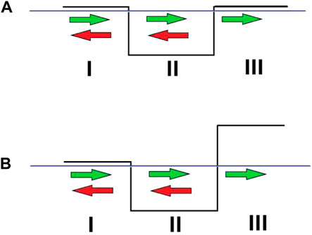
FIGURE 1. (A) Symmetric and (B) asymmetric potential well [63].
Motivated by the work studied by Pereira et al. [1], we have theoretically constructed the potential well on the graphene sheet along the zigzag direction. The region of the graphene sheet in the potential well behaves as ZGNR as in our previous work [3, 58]. The electrostatic potential profile for a potential well with a Heaviside step function (Θ(x)) is defined as [3]
where Θ(x) is defined as
Therefore, using Eq. 1, 2, potential well can be defined as [3]
Here, V0 and L represent the depth and length of the potential well, respectively. As shown in Figure 1, the electron confined in region (II) behaves as a quantum dot. Generally, conductance is expressed in terms of tunneling probability, which is defined as the ratio of the flux of a transmitted wave to that of an incident wave [51, 60]. The tunneling probability depends on the applied potential, the energy of the electron, and the width of the quantum well [60].
We have used the TBGF formalism to calculate the transport properties of ZGNR in the confined region of the potential well [3]. The symmetric and asymmetric potential wells are created simply by using the Heaviside function as shown in previous works [3, 58]. We can see from Figure 1 that there are three regions of the well. The hexagonal unit cell with N = 12 (effective number of atoms per unit cell) is shown in Figure 2 and the hexagonal structure with a basis of two atoms A and B is shown in Figure 3. The Hamiltonian in the confined region can be written as
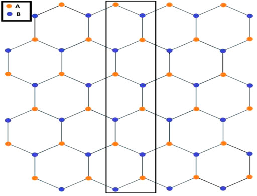
FIGURE 2. Hexagonal unit cell with N = 12 atoms (as shown in rectangle) [3].
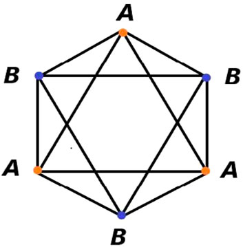
FIGURE 3. Hexagonal structure with a basis of two atoms, A and B [3].
Here, k in Eq. 4 tells us about the confined region. If some real parameter (α) replaces the phase factor, it would be in the outer regions I and III rather than in the confined region (II) of the well. H0,0 accounts for the unit cells that interact among themselves. H0,1 and H1,0 mean that the unit cell having the name 0 is interacting with 1 or vice versa. We have considered nearest neighbor interaction only. Therefore, the sparse Hamiltonian becomes like a tridiagonal [3]. We have obtained the electronic band structure by diagonalizing the Hamiltonian given in Eq. 4 and plotting it with k. The band structure for small and large N is shown in Figure 4.

FIGURE 4. ZGNR band structure (A) for small N and (B) for large N.
We have calculated the transmission coefficient and LDOS with the help of Green’s function approach here. This method, based on a tight-binding model, is a numerical method used to simulate transport properties in graphene [56, 61]. The Green’s function of a system is given by
where H is the Hamiltonian of the entire structure [3, 62]. The complete Hamiltonian of the system can be defined as
Here, HL(R) represents the Hamiltonian of the isolated left (right) lead, HD is the Hamiltonian of the system (device) without leads, and HLD (HRD) represents the interaction Hamiltonian between the device and leads.
In our calculations we have used the terms N (effective number of atoms per unit cell), M (number of unit cells), Vl (height of the potential well on the left side) and Vr (height of the potential well on the right side). The values of Vl and Vr will decide whether the potential well is symmetric or asymmetric. When Vl = Vr, the potential well is symmetric otherwise asymmetric. The system Green’s functions can be expressed as
With the help of Eqs. 5–7, we get
Therefore, using Eqs. 8–10, the device Green’s function can be described as
where ΣL and ΣR are the self-energy terms due to the coupling of semi-infinite leads and defined as
Here,
where H0,0, H−1,0, respectively, represent the tight-binding Hamiltonian of a unit cell and the coupling between two adjacent unit cells in lead. The transfer matrices (T and
where, to define ti and
with
This process is repeated until ti
where ΓL and ΓR are the corresponding broadening matrices for regions I and II, respectively, and can be written as
and Gr is the corresponding retarded Green’s function, whereas
Here, Gr and Ga differ from each other by the sign of an infinitesimally small quantity.
LDOS in terms of Green’s function can be calculated by the formula [19]
The Fano factor is expressed in terms of tunneling probability (Tn) [51, 68] and is defined by [57]
Here, Nmax is the maximum of propagating modes in the case of leads. By knowing the Fano factor, we can also calculate shot noise power (S), which can be defined as [48]
where S (0), ⟨I⟩, and e represent the shot noise at zero frequency, the total average current through the device, and the elementary charge unit, respectively. The conductance (G) is calculated by summing Tn over the modes.
where
where L and W represent the length and width of the device, respectively.
It is difficult to make GNRs with pure zigzag and armchair edges, so most GNRs produced in experiments have chiral edge geometries that include both zigzag and armchair sites [69]. In GNRs, both the geometry of the edges and their width are given by the chiral vector C. This vector is defined as [70]
where a1 and a2 are the graphene’s lattice vectors and n, m are the integers. Mechanical and electrical properties of chiral GNRs have been observed theoretically as well as experimentally [71, 72]. It has been revealed that chirality can be used to tune the electrical properties of GNRs [69, 72, 73]. A chiral vector (n, m) or chiral angle θc is used to characterize the chirality of GNRs. For the declaration of the GNR type, a beginning point known as the origin of the chiral vector is required. The GNRs are classified as type-A or type-B based on the origin point of the chiral vector. GNR is said to be type-A if the tail of the chiral vector is fixed at the center of a carbon atom positioned at sublattice A within the unit cell. If the tail of the chiral vector is fixed at the center of a carbon atom positioned at the B sublattice within the unit cell, GNR is said to be type-B. ZGNR has a chirality vector (n, n), i.e., n = m, whereas in armchair graphene nanoribbon (AGNR), chirality is defined by (n, 0) [70]. The transport vector (T) lies perpendicular to the chiral vector and can be written as [70]
where p and q are integers. The chiral angle θc in terms of n and m can be defined as [71]
The values of θc = 0° and 30° define pure zigzag and armchair edges, respectively. When the value of θc lies between 0° and 30°, the chiral nanoribbons are formed. For θc = 0°, the chiral and transport vectors lie along the armchair and zigzag directions, respectively. Thus, the ribbon with zigzag edges is formed along the transport vector direction, i.e., ZGNR. For θc = 30°, the directions of these vectors interchange and form the armchair edges along with the transport vector direction, i.e., AGNR [70, 71].
Theoretically, we study LDOS, Fano factor, shot noise and conductivity of ZGNR for different cases like symmetric and asymmetric potential wells. We have employed the TBGF approach to investigate the transport properties of ZGNRs. We have calculated LDOS in different cases, and it is observed from Figure 5 and Figure 6 that edge states occur in this system [74]. In the symmetric potential well (Vl = Vr) (Figure 5A), perfect edge states occur when N = 80 and M = 30. When we increased N up to 120 in a symmetric well and kept M fixed, edge states disappeared from the system. So, we conclude here that edge states depend on N. We further increased our N = 180 and 240 and kept the other parameters the same, like Vl, Vr, and M. It is clear from the observed results that edge states are not there. We can see that edge states, also called surface states, exist in this system, which is very well known. These states result from zigzag edges, which have localized non-dispersive states at the Fermi energy [75]. In a particular case when N = 80, M = 30, and the well is symmetric (with potential heights Vl = Vr = 50 meV), edge states are present in this geometry. We have further increased N and varied the width of the well by keeping the potential well symmetric; still, perfect edge states remain present in this system (Figure 5A). When we have kept all parameters the same and made the potential well asymmetric (with potential heights of Vl = 50 meV and Vr = 80 meV on the left and right side of the well), edge states are no longer there. It proves that edge states depend upon N and the nature of the potential well (Figure 6). Also, the asymmetric nature of LDOS arises due to the increase in the value of N and M in the symmetric potential well. In our previous work, in Figure 3 of Ref. [58], we have observed the symmetric behavior of the LDOS in the symmetric potential well. The presence of peaks in the density of state (van-Hove singularities) is frequent in one-dimensional (1D) materials, but it is not always related to edge states. van-Hove singularities appear in DOS but no edge state is present; all depends on where the states localize.
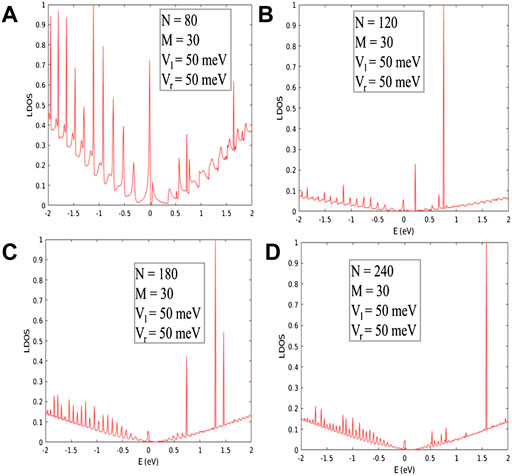
FIGURE 5. LDOS for symmetric potential well with (A) N = 80, (B) N = 120, (C) N = 180, and (D) N = 240.
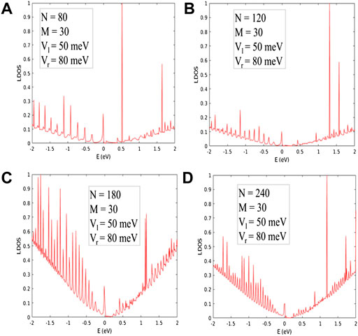
FIGURE 6. LDOS for asymmetric potential well with (A) N = 80, (B) N = 120, (C) N = 180, and (D) N = 240.
The calculated values of the Fano factor for different cases are shown in Table 1. When we keep the potential well symmetric as shown in Figure 1A, with a potential height of 50 meV on each side and taking N = 80, M = 30. We see from our data that the maximum value of F is approximately 1. Even though we have changed the potential well to asymmetric (Figure 1B) (Vl = 50 meV and Vr = 80 meV) and kept all other parameters unchanged, but the value of the Fano factor does not exceed 1 (Table 1). Our calculations show that F is always below 1, which is physically accepted also [76, 77].
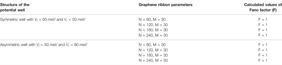
TABLE 1. Calculated values of Fano factor for different cases.
Therefore, we can conclude that the maximum possible current fluctuation for our system at low energy is limited to the mean current. The F = 1 case arises due to the transportation of a maximum number of non-interacting electrons and is known as the Poisson limit, where Pauli’s principle is not functional [52]. As we increase the energy, the Fano factor value decreases. This decrease in the value of the Fano factor is attributed to an increase in several interacting electrons. As per Pauli’s interaction, two electrons cannot occupy the same state. Therefore, the Fano factor value is not more than 1 [52]. The larger value of the Fano factor corresponds to the minimum conductivity. However, we have taken two different cases, when the left potential is not equal to the right potential and vice versa. We further calculated shot noise in our simulations [48]. It is visible from Figure 7 that when N = 20, M = 30 and the potential well is symmetric, a long peak (
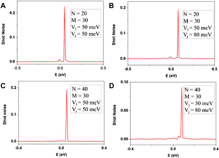
FIGURE 7. Shot noise power for (A) symmetric potential well with N = 20, (B) asymmetric well with N = 20, (C) symmetric potential well with N = 40, and (D) asymmetric potential well with N = 40.
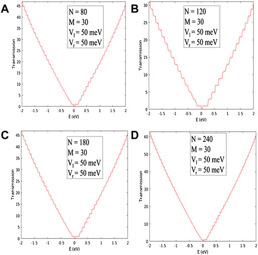
FIGURE 8. Transmission for symmetric potential well with (A) N = 80, (B) N = 120, (C) N = 180, and (D) N = 240.
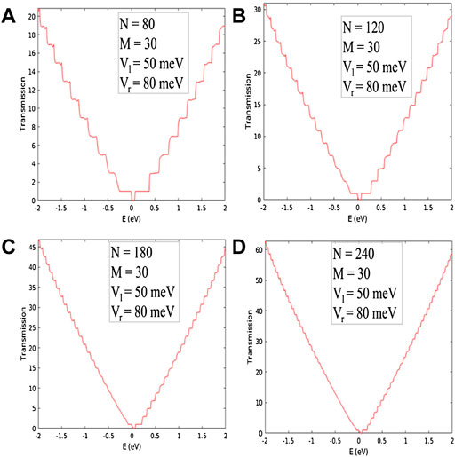
FIGURE 9. Transmission for asymmetric potential well with (A) N = 80, (B) N = 120, (C) N = 180, and (D) N = 240.
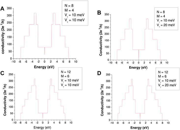
FIGURE 10. Conductivity for (A) symmetric potential well with N = 8, (B) asymmetric well with N = 8, (C) symmetric potential well with N = 12, and (D) asymmetric potential well with N = 12.
We have done our simulation for ZGNR (type-A & type-B) with the nanohub software (CNTbands) of Purdue University [4]. With the help of nanohub software, we have considered edge effects in both types (type-A & type-B) of ZGNR by varying chirality. We have calculated the density of states, band structure, and spin-resolved density in the presence or absence of edge effects. In type-A ZGNR with chirality (7,7) (Figure 11), when no edge effects are considered, the system shows perfect edge states. The presence of these edge states is reflected by the formation of the sharp peak at zero energy, as shown in Figure 11B. Also, in the absence of edge effects, the band structure remains degenerate at zero energy (Figure 11C). This shows the metallic behavior of the ribbon. These results exactly match the results obtained in the preceding section without taking into account the edge effects (See Figures 4, 5A).
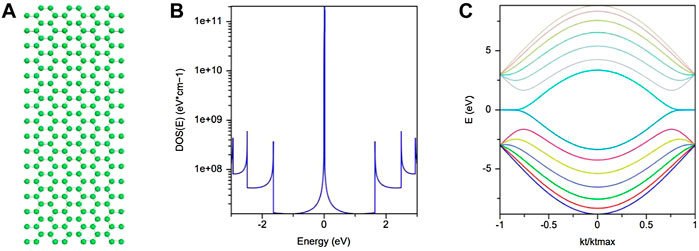
FIGURE 11. When edge effects are not considered, (A) GNR type-A with tight-binding energy (3 eV), c-c spacing (1.42 A°), chirality (7,7), (B) density of state plotted with energy, and (C) band structure. We have plotted these results from the nanohub software of Purdue University [4].
Next, we considered the type-A ZGNR with chirality (8,8) and considered the edge effects (Figure 12). The increase in chirality only changes the width of the ribbon, i.e., the number of atoms in the width of GNR. As a result, the number of subbands in the energy spectrum increases. The bandgap appears in the energy spectrum when edge effects are considered, as shown in Figure 12D, and no sharp peak appears in the density of state at zero energy (Figure 12B). In the presence of the edge effects due to spontaneous magnetic ordering, the opposite spin states accumulate at the edges of the ribbons. The interaction between these spin-polarized states gives rise to a bandgap opening in system [22]. For type-A, the variation in the spin-resolved density (Ne) of these states at different edges with atomic index is shown in Figure 12C. It can be seen that as we move from one edge to another, i.e., atom index increases, one kind of the spin density (spin up or spin down, as shown by blue or red color (Figure 12C) decreases, whereas the opposite kind increases. The interaction between these opposite spin-polarized edge states lifts the degeneracy of the zero flat bands and produces a band gap [22]. Therefore, in type-A ZGNR, a change in chirality only changes the number of subbands in the energy spectrum when edge effects are not considered. In contrast, the presence of the edge effect changes the behavior of the ribbon, that is, from metallic to semiconducting.
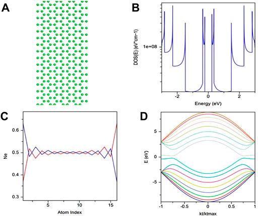
FIGURE 12. When edge effects are considered, (A) GNR type-A with tight-binding energy (3 eV), c-c spacing (1.42 A°), chirality (8,8), (B) density of states plotted with energy, (C) spin resolved density with atom index, and (D) band structure. We have plotted these results from the nanohub software of Purdue University [4].
In type-B GNRs having chirality (8,8), when edge effects are absent, no spin splitting of the edge states occurs. The band structure remains degenerate at zero energy, as shown in Figure 13C. The edge states remain in the system, which is clearly shown by the peak in the density of state at zero energy (Figure 13B). Therefore, a change in the ribbon type does not affect the presence of edge states when edge effects are not considered, and the system remains metallic. When edge effects are considered in type-B ZGNR with chirality (8,8), the accumulation of the opposite spin states occurs at the opposite zigzag edges of the ribbon. Here also, the interaction between opposite spin-polarized edge states gives rise to a finite gap in the energy spectrum (Figure 14D) of the system, which was absent before [22]. In the density of state behavior shown in Figure 14B, due to the presence of edge effects, no sharp peak appears at zero energy. The spin-resolved densities of the opposite kind formed at the opposite edges of the ribbon in the presence of edge effects. The behavior of the spin-resolved density with atom index is shown in Figure 14C. It is clear from Figure 14C that these densities decrease as we move away from the edges, i.e., from the edge to the center of the ribbon. Therefore, changes in the type and chirality of the ZGNRs only change the number of subbands and do not affect the existence of the edge states in the system when edge effects are absent. However, in the energy spectrum of both types of ribbons having different chirality, finite band gap opening takes place due to edge effects. The behavior of the spin-resolved densities is independent of type-A or type-B ZGNR, and these densities decrease for both types as we move away from the edge toward the ribbon center.
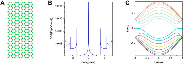
FIGURE 13. When edge effects are not considered (A) GNR type-B with tight-binding energy (3 eV), c-c spacing (1.42 A°), chirality (8,8), (B) density of state plotted with energy, and (C) band structure. We have plotted these results from the nanohub software of Purdue University [4].
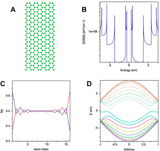
FIGURE 14. When edge effects are considered, (A) GNR type-B with tight-binding energy (3 eV), c-c spacing (1.42 A°), chirality (8,8), (B) density of states plotted with energy, (C) spin resolved density with atom index, and (D) band structure. We have plotted these results from the nanohub software of Purdue University [4].
To summarize, we have numerically investigated the quantum transport behavior of ZGNRs in the confined region of the potential well. In the symmetric potential well, the study reveals that perfect edge states appear when N = 80 and M = 30, and disappear when N = 120, and M = 30. Also, in the case of the asymmetric potential well, no edge states appear in the system when N = 80, 120 and M = 30. Therefore, the existence of the edge states depends on N and the type of the potential well (symmetric or asymmetric). The presence of edge states at zero Fermi energy exhibit van-Hove singularity in DOS. No van-Hove singularity appears at zero Fermi energy in the presence of edge effects. Therefore, at zero Fermi energy, the presence of edge states is associated with the van-Hove singularity in DOS. Moreover, perfect conductance/conductivity plateaus are observed in both symmetric and asymmetric potential wells. However, a dip appears in the conductivity at zero Fermi energy in the symmetric case only. For symmetrical and asymmetrical potential wells, we found that the Fano factor is approximately 1, which corresponds to the minimum conductivity. Also, the value of the Fano factor does not exceed one, which is physically acceptable [54, 76, 77].
On the other hand, the results obtained from the nanohub show the existence of edge states in the absence of edge effects, and the system shows metallic behavior. In the presence of edge effects (both type-A and type-B GNRs), the magnetic ordering between spin-polarized states gives rise to band gap opening in the energy spectrum. Therefore, the system shows semiconducting behavior in the presence of edge effects. Moreover, in the absence of edge effects, the increase in the chirality (n, n) of both GNRs (type-A & type-B) does not change the behavior of the system except by adding more subbands to the band structure.
The original contributions presented in the study are included in the article/Supplementary Material; further inquiries can be directed to the corresponding author.
All the authors listed have made a substantial, direct, and intellectual contribution to the work and approved it for publication.
The authors declare that the research was conducted in the absence of any commercial or financial relationships that could be construed as a potential conflict of interest.
All claims expressed in this article are solely those of the authors and do not necessarily represent those of their affiliated organizations, or those of the publisher, the editors, and the reviewers. Any product that may be evaluated in this article, or claim that may be made by its manufacturer, is not guaranteed or endorsed by the publisher.
The authors would like to thank Prof. S. S. Kubakaddi at K.L.E. Technological University, Hubballi, Karnataka, India for their valuable discussion during the course of this work.
1. Pereira JM, Mlinar V, Peeters F, Vasilopoulos P. Confined States and Direction-Dependent Transmission in Graphene Quantum Wells. Phys Rev B (2006) 74:045424. doi:10.1103/physrevb.74.045424
2. Shakouri K, Masir MR, Jellal A, Choubabi EB, Peeters FM. Effect of Spin-Orbit Couplings in Graphene with and without Potential Modulation. Phys Rev B (2013) 88:115408. doi:10.1103/physrevb.88.115408
3. Pratap S. Transport Properties of Zigzag Graphene Nanoribbons in the Confined Region of Potential Well. Superlattices and Microstructures (2016) 100:673–82. doi:10.1016/j.spmi.2016.10.031
5. Han W, Kawakami RK, Gmitra M, Fabian J. Graphene Spintronics. Nat Nanotech (2014) 9:794–807. doi:10.1038/nnano.2014.214
6. Mahmoudi T, Wang Y, Hahn Y-B. Graphene and its Derivatives for Solar Cells Application. Nano Energy (2018) 47:51–65. doi:10.1016/j.nanoen.2018.02.047
7. Ruffieux P, Wang S, Yang B, Sánchez-Sánchez C, Liu J, Dienel T, et al. On-surface Synthesis of Graphene Nanoribbons with Zigzag Edge Topology. Nature (2016) 531:489–92. doi:10.1038/nature17151
8. Geim AK, Novoselov KS. Nanoscience and Technology: A Collection of Reviews from Nature Journals. Singapore: World Scientific (2010). p. 11–9.
9. Földi P, Molnár B, Benedict MG, Peeters F. Spintronic Single-Qubit Gate Based on a Quantum Ring with Spin-Orbit Interaction. Phys Rev B (2005) 71:033309. doi:10.1103/physrevb.71.033309
10. Enoki T, Ando T. Physics and Chemistry of Graphene: Graphene to Nanographene. Boca Raton, FL, USA: CRC Press (2019).
11. Dong HM, Xu W, Peeters FM. Electrical Generation of Terahertz Blackbody Radiation from Graphene. Opt Express (2018) 26:24621. doi:10.1364/oe.26.024621
12. Milovanović S, Tadić M, Peeters F. Graphene Membrane as a Pressure Gauge. Appl Phys Lett (2017) 111:043101. doi:10.1063/1.4995983
13. Castro Neto AH, Guinea F, Peres NMR, Novoselov KS, Geim AK. The Electronic Properties of Graphene. Rev Mod Phys (2009) 81:109–62. doi:10.1103/revmodphys.81.109
14. Liang X, Jung Y-S, Wu S, Ismach A, Olynick DL, Cabrini S, et al. Formation of Bandgap and Subbands in Graphene Nanomeshes with Sub-10 Nm Ribbon Width Fabricated via Nanoimprint Lithography. Nano Lett (2010) 10:2454–60. doi:10.1021/nl100750v
15. Seol G, Guo J. 2011 International Electron Devices Meeting. Manhattan, New York: IEEE (2011). p. 2–3.
16. Ni ZH, Yu T, Lu YH, Wang YY, Feng YP, Shen ZX. Uniaxial Strain on Graphene: Raman Spectroscopy Study and Band-Gap Opening. ACS nano (2008) 2:2301–5. doi:10.1021/nn800459e
17. Baringhaus J, Edler F, Tegenkamp C. Edge-states in Graphene Nanoribbons: a Combined Spectroscopy and Transport Study. J Phys Condens Matter (2013) 25:392001. doi:10.1088/0953-8984/25/39/392001
18. Han MY, Özyilmaz B, Zhang Y, Kim P. Energy Band-Gap Engineering of Graphene Nanoribbons. Phys Rev Lett (2007) 98:206805. doi:10.1103/physrevlett.98.206805
19. Bhalla P, Pratap S. Aspects of Electron Transport in Zigzag Graphene Nanoribbons. Int J Mod Phys B (2018) 32:1850148. doi:10.1142/s0217979218501485
20. Chen Y-C, De Oteyza DG, Pedramrazi Z, Chen C, Fischer FR, Crommie MF. Tuning the Band Gap of Graphene Nanoribbons Synthesized from Molecular Precursors. ACS nano (2013) 7:6123–8. doi:10.1021/nn401948e
21. Kosynkin DV, Higginbotham AL, Sinitskii A, Lomeda JR, Dimiev A, Price BK, et al. Longitudinal Unzipping of Carbon Nanotubes to Form Graphene Nanoribbons. Nature (2009) 458:872–6. doi:10.1038/nature07872
22. Son Y-W, Cohen ML, Louie SG. Energy Gaps in Graphene Nanoribbons. Phys Rev Lett (2006) 97:216803. doi:10.1103/physrevlett.97.216803
23. Deng H-Y, Wakabayashi K. Edge Effect on a Vacancy State in Semi-infinite Graphene. Phys Rev B (2014) 90:115413. doi:10.1103/physrevb.90.115413
24. Wakabayashi K, Sasaki K-i., Nakanishi T, Enoki T. Electronic States of Graphene Nanoribbons and Analytical Solutions. Sci Technol Adv Mater (2010) 11:054504. doi:10.1088/1468-6996/11/5/054504
25. Areshkin DA, Gunlycke D, White CT. Ballistic Transport in Graphene Nanostrips in the Presence of Disorder: Importance of Edge Effects. Nano Lett (2007) 7:204–10. doi:10.1021/nl062132h
26. Koch M, Ample F, Joachim C, Grill L. Voltage-dependent Conductance of a Single Graphene Nanoribbon. Nat Nanotech (2012) 7:713–7. doi:10.1038/nnano.2012.169
27. Merino-Díez N, Garcia-Lekue A, Carbonell-Sanromà E, Li J, Corso M, Colazzo L, et al. Width-Dependent Band Gap in Armchair Graphene Nanoribbons Reveals Fermi Level Pinning on Au(111). ACS nano (2017) 11:11661–8. doi:10.1021/acsnano.7b06765
28. Zhang L, Xia Z. Mechanisms of Oxygen Reduction Reaction on Nitrogen-Doped Graphene for Fuel Cells. J Phys Chem C (2011) 115:11170–6. doi:10.1021/jp201991j
29. Zhang CX, He C, Xue L, Zhang KW, Sun LZ, Zhong J. Transport Properties of Zigzag Graphene Nanoribbons with Oxygen Edge Decoration. Org Electron (2012) 13:2494–501. doi:10.1016/j.orgel.2012.06.041
30. Eda G, Mattevi C, Yamaguchi H, Kim H, Chhowalla M. Insulator to Semimetal Transition in Graphene Oxide. J Phys Chem C (2009) 113:15768–71. doi:10.1021/jp9051402
31. Yu Z, Sun LZ, Zhang CX, Zhong JX. Transport Properties of Corrugated Graphene Nanoribbons. Appl Phys Lett (2010) 96:173101. doi:10.1063/1.3419821
32. Enoki T, Fujii S, Takai K. Zigzag and Armchair Edges in Graphene. Carbon (2012) 50:3141–5. doi:10.1016/j.carbon.2011.10.004
33. Majidi L, Asgari R. New Supercurrent Pattern in Quantum point Contact with Strained Graphene Nanoribbon. New J Phys (2020) 22:123033. doi:10.1088/1367-2630/abd0b7
34. Huang B, Liu F, Wu J, Gu B-L, Duan W. Suppression of Spin Polarization in Graphene Nanoribbons by Edge Defects and Impurities. Phys Rev B (2008) 77:153411. doi:10.1103/physrevb.77.153411
35. Magda GZ, Jin X, Hagymási I, Vancsó P, Osváth Z, Nemes-Incze P, et al. Room-temperature Magnetic Order on Zigzag Edges of Narrow Graphene Nanoribbons. Nature (2014) 514:608–11. doi:10.1038/nature13831
36. Kane CL, Mele EJ. Quantum Spin Hall Effect in Graphene. Phys Rev Lett (2005) 95:226801. doi:10.1103/physrevlett.95.226801
37. Kane CL, Mele EJ. Z2Topological Order and the Quantum Spin Hall Effect. Phys Rev Lett (2005) 95:146802. doi:10.1103/physrevlett.95.146802
38. Li J, Sanz S, Merino-Díez N, Vilas-Varela M, Garcia-Lekue A, Corso M, et al. Topological Phase Transition in Chiral Graphene Nanoribbons: from Edge Bands to End States. Nat Commun (2021) 12:1. doi:10.1038/s41467-021-25688-z
39. Bhalla P, Deng M-X, Wang R-Q, Wang L, Culcer D. Nonlinear Ballistic Response of Quantum Spin Hall Edge States. Phys Rev Lett (2021) 127:206801. doi:10.1103/physrevlett.127.206801
40. Wang Z, Bhalla P, Edmonds M, Fuhrer MS, Culcer D. Unidirectional Magnetotransport of Linearly Dispersing Topological Edge States. Phys Rev B (2021) 104:L081406. doi:10.1103/physrevb.104.l081406
41. Liu C, Ma W, Chen M, Ren W, Sun D. A Vertical Silicon-Graphene-Germanium Transistor. Nat Commun (2019) 10:1. doi:10.1038/s41467-019-12814-1
42. Saremi M, Saremi M, Niazi H, Goharrizi AY. Modeling of Lightly Doped drain and Source Graphene Nanoribbon Field Effect Transistors. Superlattices and Microstructures (2013) 60:67–72. doi:10.1016/j.spmi.2013.04.013
43. Shen L, Zeng M, Li S, Sullivan MB, Feng YP. Electron Transmission Modes in Electrically Biased Graphene Nanoribbons and Their Effects on Device Performance. Phys Rev B (2012) 86:115419. doi:10.1103/physrevb.86.115419
44. Lan J, Wang J-S, Gan CK, Chin SK. Edge Effects on Quantum thermal Transport in Graphene Nanoribbons: Tight-Binding Calculations. Phys Rev B (2009) 79:115401. doi:10.1103/physrevb.79.115401
45. Cayssol J, Huard B, Goldhaber-Gordon D. Contact Resistance and Shot Noise in Graphene Transistors. Phys Rev B (2009) 79:075428. doi:10.1103/physrevb.79.075428
46. Marconcini P, Logoteta D, Macucci M. Envelope-function-based Analysis of the Dependence of Shot Noise on the Gate Voltage in Disordered Graphene Samples. Phys Rev B (2021) 104:155429. doi:10.1103/physrevb.104.155429
47. Marconcini P, Macucci M. Effects of A Magnetic Field on the Transport and Noise Properties of a Graphene Ribbon with Antidots. Nanomaterials (2020) 10:2098. doi:10.3390/nano10112098
48. Blanter YM, Büttiker M. Shot Noise in Mesoscopic Conductors. Phys Rep (2000) 336:1–166. doi:10.1016/s0370-1573(99)00123-4
49. Gopar VA. Shot Noise Fluctuations in Disordered Graphene Nanoribbons Near the Dirac point. Physica E: Low-dimensional Syst Nanostructures (2016) 77:23–8. doi:10.1016/j.physe.2015.10.032
50. Danneau R, Wu F, Craciun MF, Russo S, Tomi MY, Salmilehto J, et al. Evanescent Wave Transport and Shot Noise in Graphene: Ballistic Regime and Effect of Disorder. J Low Temp Phys (2008) 153:374–92. doi:10.1007/s10909-008-9837-z
51. Soliman W, Asham MD, Phillips AH. Fano Factor in Strained Graphene Nanoribbon Nanodevices. Chin Phys. Lett. (2017) 34:118503. doi:10.1088/0256-307x/34/11/118503
52. Tworzydło J, Trauzettel B, Titov M, Rycerz A, Beenakker CW. Sub-Poissonian Shot Noise in Graphene. Phys Rev Lett (2006) 96:246802. doi:10.1103/PhysRevLett.96.246802
53. Dragomirova RL, Areshkin DA, Nikolić BK. Shot Noise Probing of Magnetic Ordering in Zigzag Graphene Nanoribbons. Phys Rev B (2009) 79:241401. doi:10.1103/physrevb.79.241401
54. Tan ZB, Puska A, Nieminen T, Duerr F, Gould C, Molenkamp LW, et al. Shot Noise in Lithographically Patterned Graphene Nanoribbons. Phys Rev B (2013) 88:245415. doi:10.1103/physrevb.88.245415
55. Bora V, Barrett HH, Fastje D, Clarkson E, Furenlid L, Bousselham A, et al. Estimation of Fano Factor in Inorganic Scintillators. Nucl Instr Methods Phys Res Section A: Acc Spectrometers, Detectors Associated Equipment (2016) 805:72–86. doi:10.1016/j.nima.2015.07.009
56. Marconcini P, Macucci M. Geometry-dependent Conductance and Noise Behavior of a Graphene Ribbon with a Series of Randomly Spaced Potential Barriers. J Appl Phys (2019) 125:244302. doi:10.1063/1.5092512
57. Nascimento ACS, Lima RPA, Lyra ML, Lima JRF. Electronic Transport on Graphene Armchair-Edge Nanoribbons with Fermi Velocity and Potential Barriers. Phys Lett A (2019) 383:2416–23. doi:10.1016/j.physleta.2019.04.052
58. Pratap S, Kumar V. Dirac Fermions in Zigzag Graphene Nanoribbon in a Finite Potential Well. Physica B: Condensed Matter (2021) 614:412916. doi:10.1016/j.physb.2021.412916
60. Sakurai J, Napolitano J, Modern Quantum Mechanics. Cambridge: Cambridge University Press (2017). p. 386–445.
61. Lewenkopf CH, Mucciolo ER. The Recursive Green's Function Method for Graphene. J Comput Electron (2013) 12:203–31. doi:10.1007/s10825-013-0458-7
62. Pratap S. Transmission and LDOS in Case of ZGNR with and without Magnetic Field. Superlattices and Microstructures (2017) 104:540–6. doi:10.1016/j.spmi.2017.02.046
63. Katsnelson MI, Iosifovich M. Graphene: Carbon in Two Dimensions. Cambridge: Cambridge University Press (2012).
64. Sancho MPL, Sancho JML, Sancho JML, Rubio J. Highly Convergent Schemes for the Calculation of Bulk and Surface Green Functions. J Phys F: Met Phys (1985) 15:851–8. doi:10.1088/0305-4608/15/4/009
65. Nardelli MB. Electronic Transport in Extended Systems: Application to Carbon Nanotubes. Phys Rev B (1999) 60:7828–33. doi:10.1103/physrevb.60.7828
66. Farokhnezhad M, Esmaeilzadeh M, Ahmadi S, Pournaghavi N. Controllable Spin Polarization and Spin Filtering in a Zigzag Silicene Nanoribbon. J Appl Phys (2015) 117:173913. doi:10.1063/1.4919659
68. Yuan J-H, Cheng Z, Zhang J-J, Zeng Q-J, Zhang J-P. Voltage-driven Electronic Transport and Shot Noise in Armchair Graphene Nanoribbons. Phys Lett A (2011) 375:2670–5. doi:10.1016/j.physleta.2011.05.064
69. Ritter KA, Lyding JW. The Influence of Edge Structure on the Electronic Properties of Graphene Quantum Dots and Nanoribbons. Nat Mater (2009) 8:235–42. doi:10.1038/nmat2378
70. Dass D. Structural Analysis, Electronic Properties, and Band Gaps of a Graphene Nanoribbon: A New 2D Materials. Superlattices and Microstructures (2018) 115:88–107. doi:10.1016/j.spmi.2018.01.001
71. Tabarraei A, Shadalou S, Song J-H. Mechanical Properties of Graphene Nanoribbons with Disordered Edges. Comput Mater Sci (2015) 96:10–9. doi:10.1016/j.commatsci.2014.08.001
72. Tao C, Jiao L, Yazyev OV, Chen Y-C, Feng J, Zhang X, et al. Spatially Resolving Edge States of Chiral Graphene Nanoribbons. Nat Phys (2011) 7:616–20. doi:10.1038/nphys1991
73. Berahman M, Asad M, Sanaee M, Sheikhi MH. Optical Properties of Chiral Graphene Nanoribbons: a First Principle Study. Opt Quant Electron (2015) 47:3289–300. doi:10.1007/s11082-015-0207-1
74. Pratap S. AIP Conference Proceedings. Melville, NY: AIP Publishing LLC (2020). p. 100011. vol. 2220.
75. Lado JL, García-Martínez N, Fernández-Rossier J. Edge States in Graphene-like Systems. Synth Met (2015) 210:56–67. doi:10.1016/j.synthmet.2015.06.026
76. Logoteta D, Marconcini P, Macucci M. 2013 22nd International Conference on Noise and Fluctuations (ICNF). Manhattan, New York: IEEE (2013). p. 1–4.
Keywords: Fano factor, shot noise, transport properties, graphene nanoribbon, transmission
Citation: Pratap S, Kumar S and Singh RP (2022) Certain Aspects of Quantum Transport in Zigzag Graphene Nanoribbons. Front. Phys. 10:940586. doi: 10.3389/fphy.2022.940586
Received: 10 May 2022; Accepted: 13 June 2022;
Published: 15 July 2022.
Edited by:
Santanu K. Maiti, Indian Statistical Institute, IndiaReviewed by:
Leyla Majidi, Institute for Research in Fundamental Sciences (IPM), IranCopyright © 2022 Pratap, Kumar and Singh. This is an open-access article distributed under the terms of the Creative Commons Attribution License (CC BY). The use, distribution or reproduction in other forums is permitted, provided the original author(s) and the copyright owner(s) are credited and that the original publication in this journal is cited, in accordance with accepted academic practice. No use, distribution or reproduction is permitted which does not comply with these terms.
*Correspondence: Surender Pratap, c3VyZW4xOTg2ZGhhbGFyaWFAaHBjdS5hYy5pbg==
Disclaimer: All claims expressed in this article are solely those of the authors and do not necessarily represent those of their affiliated organizations, or those of the publisher, the editors and the reviewers. Any product that may be evaluated in this article or claim that may be made by its manufacturer is not guaranteed or endorsed by the publisher.
Research integrity at Frontiers
Learn more about the work of our research integrity team to safeguard the quality of each article we publish.