 Chengtao Jiang
95% of researchers rate our articles as excellent or good
Learn more about the work of our research integrity team to safeguard the quality of each article we publish.
Find out more
ORIGINAL RESEARCH article
Front. Phys. , 03 November 2021
Sec. Optics and Photonics
Volume 9 - 2021 | https://doi.org/10.3389/fphy.2021.768192
This article is part of the Research Topic Advances in Terahertz Detection and Imaging View all 15 articles
In this study, we demonstrate an Nb5N6 terahertz (THz) detector with radio frequency (RF) choke-enhanced dipole antenna structure for 0.3 THz detection. The maximum electric field intensity of 218 V/m is obtained by optimizing the parameters of the dipole antenna with RF choke. Compared to a dipole antenna without RF choke, the electric field intensity of that with RF choke is improved by 2.6 times. The RF choke-enhanced dipole antenna-coupled Nb5N6 THz detector is fabricated and characterized. The measured maximum responsivity of the detector is 1100 V/W at 0.308 THz, and the corresponding noise equivalent power (NEP) is 6.4 × 10⁻¹² W/Hz1/2. The measured response time of the Nb5N6 THz detector is as low as 8.46 μs. Furthermore, the Nb5N6 THz detector is applied to a homemade THz transmission imaging system for demonstrating its performance. The THz imaging results of a blade and access card show that the contrast of the blade image is sharp and the components hidden within the access card are clearly visible. This indicates that the Nb5N6 THz detector can be used in THz imaging, particularly in THz active imaging, which will have greater application prospects.
In recent years, with the development of science and technology, the terahertz (THz) waves have attracted worldwide interest. THz technology is applicable in many fields such as physics, life science, materials science, astronomy, information technology, and national defense security. THz detectors are crucial components in terahertz technology, which have extensive application prospects in spectrum analysis, medical imaging, radio astronomy, security checks, biosensing, etc. [1–6]. At present, the research on uncooled THz detectors involve Golay cells [7], Schottky diodes [8], field-effect transistors (FETs) [9], and bolometers [10–12]. Among them, bolometers have been attracting more and more attention because of easy fabrication, integration with readout circuits, high sensitivity, low-noise equivalent power (NEP), wide response spectrum, and so on. To date, several materials have been used as the bolometers, such as VOx [13–16], YBCO [17–19], titanium (Ti) [20], niobium (Nb) [10, 21], platinum (Pt) [22], poly-Si [23], poly-Si-Ge alloys [24], etc. Although polycrystalline VOx exhibits a temperature coefficient of resistance [TCR = (1/R)*(dR/dT)] ∼ −2%/K] at room temperature, it undergoes a semiconductor-metal transition at ∼ 67°C, which reduces the dynamic range of the bolometer when working in the semiconductor phase [25]. Amorphous YBCO has been demonstrated as an uncooled bolometer, but its stoichiometric composition is difficult to control, and the resistance and TCR are affected by the oxygen concentration in films [26]. The low TCR value of metallic materials (two orders of the magnitude lower than that of semiconductors) results in low responsivity of detectors. In polycrystalline Si and Si-Ge alloys, the resistivity can be maintained sufficiently low by controlling the doping level, although it limits the TCR to approximately 2.5–3%/K. However, the processing of polycrystalline materials requires temperatures as high as 650°C for achieving the desired crystallinity [23, 24]. Therefore, it is desirable to combine the advantages of both semiconductors (high TCR for high responsivity) and metals (low resistivity) for the development of fast and sensitive THz detectors.
The Nb5N6 films made in our laboratory exhibit a high TCR of 0.7%/K, which is higher than that of metals [27–29]. In addition, the resistivity of Nb5N6 (<5 × 10⁻³ Ω cm) is considerably lower than that of the other semiconductors, resulting in reduction of the impedance in comparison with a-Si or VOx devices of the same dimensions, which is advantageous to impedance matching when integrated with planar antennas. Moreover, the Nb5N6 films include other advantages, such as simple fabrication, low cost, large area production, and easy control. Hence, Nb5N6 thin films are promising candidate material for THz bolometer detector at room temperature.
Generally, a THz bolometer detector consists of a THz antenna and a thin film microbridge. As the key component of the detector, the antenna plays an important role in coupling THz radiations to the film microbridge; hence, the performance of the detector can be improved by appropriately designing and optimizing the antenna structure. Radio frequency (RF) choke structures are often used in the antenna design for improving the antenna performance, such as bandwidth enhancement, multiple band operation, gain enhancement, and radiation pattern shaping [30–33]. Their functions are usually to provide direct current (DC) bias and prevent RF signals from leaking to the bias electrodes. Considering the feature of the RF choke, we designed an RF choke-enhanced dipole antenna to improve the performance of the Nb5N6 THz detector. Compared to that without RF choke, the electric field intensity of the RF choke-enhanced dipole antenna can be significantly improved. In addition, we applied the Nb5N6 THz detector to a THz transmission imaging system and studied the THz imaging of a blade and access card.
We choose 0.3 THz as the center frequency of the dipole antenna for design and optimization, because it is located in the atmospheric transmission window of THz signals, and its loss is small in the atmosphere. To maximize the response of dipole antenna under the 0.3 THz radiation, the antenna length must match the effective wavelength of the surrounding media. The length l of the resonant antenna [34] is given by
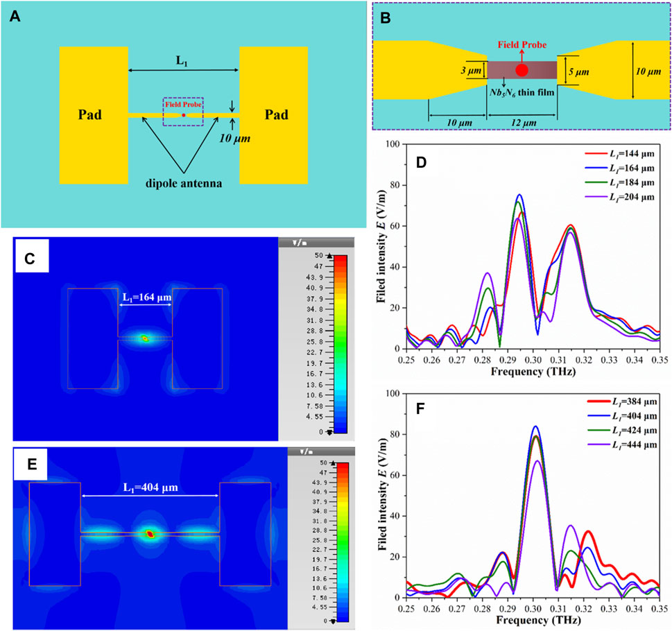
FIGURE 1. (A) Schematic diagram of the planar dipole antenna on the Si substrate. (B) The location and size of the Nb5N6 film in the planar dipole antenna. (C) The electric field intensity distribution of the half-wave dipole antenna with L1 = 164 μm at 0.295 THz. (D) The electric field intensity varies with L1 in the half-wave dipole antenna in the range of 0.25–0.35 THz. (E) The electric field intensity distribution of the full-wave dipole antenna with L1 = 404 μm at 0.301 THz. (F) The electric field intensity varies with L1 in the full-wave dipole antenna in the range of 0.25–0.35 THz.
To further enhance the electric field intensity at the center of the dipole antenna, an RF choke structure was employed to prevent the coupled THz waves from leaking to the bias pads, as depicted in Figure 2A. By optimizing the location and the size of the RF choke, a maximum electric field intensity of 218 V/m at the center of the dipole antenna with RF choke is obtained at 0.301 THz, as shown in Figure 2B. The optimized parameters of the dipole antenna with RF choke are as follows: L2 = 66 μm, W1 = 30 μm, and W2 = 230 μm. Compared to the dipole antenna without RF choke, the maximum electric field intensity is improved by 2.6 times. The electric field intensity distribution of the antenna with RF choke near the surface of the Si substrate at 0.301 THz is displayed in Figure 2C. The antenna gap region has greater local field enhancement due to the suppression effect of RF choke structure. There is almost no electric field distribution on the bias pads, and the electric field is mainly concentrated between RF choke structures, which makes the electric field intensity at the center of the dipole antenna greater. When the RF choke-enhanced dipole antenna is integrated with the Nb5N6 microbolometer THz detector, the Nb5N6 film can absorb more THz energy, thus improving the sensitivity of the device. Figure 2D shows the far-field radiation patterns of the dipole antenna with RF choke in the E plane (Phi = 0°) and H plane (Phi = 0°) at 0.301 THz, with a maximum directivity of 8.34 dBi. This indicates that the dipole antenna with RF choke has a good property of receiving the normal incidence THz waves according to the reciprocity principle.
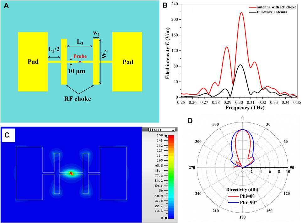
FIGURE 2. (A) Schematic diagram of the dipole antenna with RF choke on the Si substrate. (B) The curve of the electric field intensity varies with the frequency of the dipole antenna with or without RF choke. (C) The electric field intensity distribution of the dipole antenna with RF choke near the surface of the Si substrate at 0.301 THz. (D) The radiation patterns of the planar dipole antenna with RF choke at 0.301 THz.
The fabrication of the RF choke-enhanced dipole antenna-coupled Nb5N6 microbolometer THz detector was implemented using micromachining technique. The process flow is illustrated in Figure 3. The Nb5N6 film with a thickness of 120 nm was first deposited on the thermally oxidized Si substrate by using RF magnetron sputtering, as shown in Figure 3A. The TCR of the Nb5N6 thin film is −0.7% K−1 at 300 K. After the required pattern was formed through micro-processing technology, 5 nm thick Ti membrane and a 200 nm thick Au membrane were deposited on the formed pattern (Figure 3B) and the Ti membrane function as an adhesive layer in this process. Further, the Au antenna pattern was formed by using the lift-off technology, as shown in Figure 3C. Subsequently, the Nb5N6 thin film was patterned into Nb5N6 film microbridge using lithography and reactive ion etching (RIE) technique (Figure 3D). The resistance of the Nb5N6 microbolometer THz detector depends on the dimensions of the Nb5N6 film microbridge. Finally, a photoresist protection pattern was generated on the formed pattern using the same lithography technique, with only two open areas on both sides of the Nb5N6 film microbridge (Figure 3E). After the photoresist pattern was formed, the SiO2 layer on the surface of the Si substrate was dry-etched through RIE to expose Si pattern only in the two open areas. The RIE was performed in a gas mixture of CF4 and O2 at the total pressure of 4 Pa and RF power of 150 W for 3 min. The optimized mixture ratio of CF4 and O2 was 30:10. The opening formed on Si was further etched by using RIE to create an air-cavity (Figure 3F). The etching conditions are as follows: the flow of SF6 is 40 sccm, chamber pressure is 8 Pa, and the RF power is 70 W. The air-cavity was formed under the Nb5N6 film microbridge with a SiO2 supporting layer through RIE etching, because the etching rate of Si was much higher than that of SiO2. In the etching process of the Si air-cavity, we adopted the technology of stepwise etching, etching for 3 min each step, and etching for three steps in total. The advantages of stepwise etching are that, on the one hand, it is conducive to directly observe whether the air-cavity under the Nb5N6 film microbridge is formed; on the other hand, when the air-cavity is etched, the photoresistance on the surface of Si substrate will be heated as little as possible to prevent it from solidifying, which is conducive to the removal of photoresistance in the later stage.
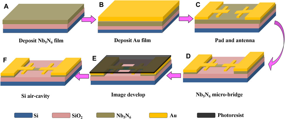
FIGURE 3. The fabrication process of the Nb5N6 THz detector integrated with RF choke-enhanced dipole antenna.
The optical image of the fabricated RF choke-enhanced dipole antenna-coupled Nb5N6 THz detector and the SEM micrograph of an Nb5N6 air-bridge are displayed in Figure 4. The fabricated Nb5N6 THz detector includes four main parts: a planar dipole antenna, Au bias pads, an Nb5N6 film microbridge, and an etched air-cavity. In Figure 4B, the Nb5N6 film microbridge is thoroughly freestanding from the Si substrate with a 200 nm SiO2 support layer. The SiO2 layer mainly plays a role in preventing the Nb5N6 film microbridge from fracture or collapse. The air-cavity isolates the heat conduction between the Nb5N6 film microbridge and the Si substrate, which further improves the sensitivity of the THz detector. The DC resistance of the fabricated Nb5N6 THz detector is 0.76 kΩ.
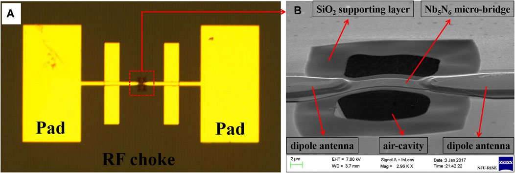
FIGURE 4. (A) Image of the fabricated antenna-coupled Nb5N6 THz detector. (B) SEM micrograph of the Nb5N6 air-bridge.
Typical performance parameters of THz detectors are responsivity (
where △U is the output voltage of the Nb5N6 THz detector, Pin is the input power received on the effective area of the Nb5N6 THz detector, and Sbeam and Pbeam are the spot size and total power of the THz beam at the focus, respectively. The measured total power of the THz beam at the focus is 0.5 mW.
Measuring the power received by the detector is essential to calculate responsivity and NEP, but this power is a function of effective area Aeff and impinging of received power density. The effective area Aeff is considered as the pixel area that effectively captures the impinging power and it is a function of receiving antenna directivity and signal frequency. Thus, if D is the directivity of receiving antenna, the effective area of the THz detector is given by [37, 38]
where λ is the signal wavelength. For a simulated value of D = 8.6 dBi and free-space wavelength λ = 0.97 mm at 0.301THz, a value of Aeff = 0.516 mm2 is obtained.
To calculate the power on the effective receiving area of the Nb5N6 THz detector, it is necessary to determine the spot size of the THz beam on the focal plane. The spot distribution of the THz beam at the focus is scanned using the Nb5N6 THz detector. At a scan range of 20 mm × 20 mm and the step size of 210 μm, the measured spot distribution of the THz beam at the focus is depicted in Figure 5. Figure 5A is the three-dimensional distribution of the THz beam scanned by the Nb5N6 THz detector. The ordinate denotes the normalized response voltage value, and the X-axis and Y-axis denote the scanning distance of the Nb5N6 THz detector, respectively. A scanned image of the THz beam at the focus is displayed in Figure 5B. It can be seen that the spot diameter of the THz beam is about 10 mm.
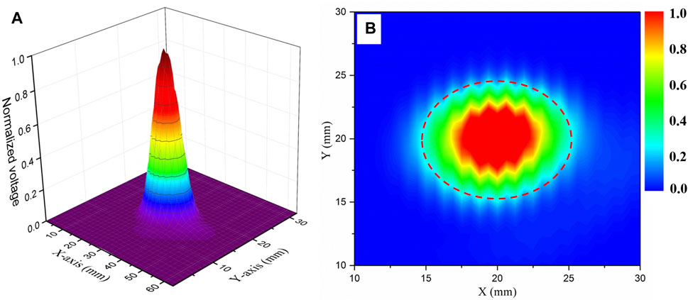
FIGURE 5. (A) 3-D image of the THz beam scanned by the Nb5N6 THz detector at 0.308 THz and (B) 2-D image of the THz beam in the focal plane.
The used THz source is composed of AMC-336 frequency multiplier produced by Virginia Diodes, Inc. (VDI) and Agilent E8251D signal generator. A low-frequency signal provided by the signal generator is amplified by AMC-336 frequency multiplier (WR2.8 VDI horn) to obtain the THz frequency in the range of 0.25–0.35 THz. The modulation signal of the signal generator is 1 kHz, which is input to the lock-in amplifier as a reference signal. The maximum output power of THz source is about 0.5 mW measured by a thermal power sensor (OPHIR, 3A-P-THz). The THz radiation is focused to maximize the electrical signal of the detector by two off-axis parabolic mirrors and the three-dimensional displacement platform. The responses voltage of the detector is read out by a lock-in amplifier (SR830). The responsivity of the Nb5N6 array detector depends on its voltage value and is calculated by Eqs 1–3. The measured optical voltage responsivity of the Nb5N6 THz detector varies with frequency, as shown in Figure 6. The resonant frequency corresponding to the maximum optical responsivity of the Nb5N6 THz detector is 0.308 THz, and the best optical responsivity is 1100 V/W. The measured responsivity varying with frequency is the same as the variation trend of simulated electric field intensity with the frequency. A small frequency shift is observed at the resonance frequency. This deviation may be due to the approximate simulation model, in which we neither considered the effect of the air-bridge nor the size deviation in the fabrication process.
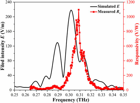
FIGURE 6. Measured optical responsivity of the Nb5N6 THz detector in the frequency range 0.25–0.35 THz.
Besides the RF responsivity, the NEP is crucial parameter for characterizing the sensitivity of THz detector, which can be expressed as
where Vnoise is the voltage noise spectral density and
The voltage noise spectral density of the Nb5N6 THz detector was obtained using a spectrum analyzer (Agilent 35670A) and a low-noise amplifier (LNA-SR560) with a voltage gain of 60 dB, as shown in Figure 7A. The noise voltage of the Nb5N6 THz detector increases with the bias current. Note that the 1/f noise cross point also increases with the increase of the bias current. At lower bias current (0 and 0.2 mA) and modulation frequencies greater than 1 and 4 kHz, the noise spectrum tends to be constant and the device is limited by the thermal noise (
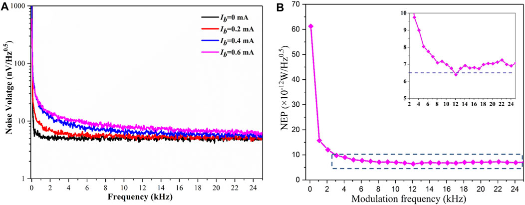
FIGURE 7. (A) Measured noise voltage under different bias currents and (B) the calculated NEP as a function of the modulation frequency for the Nb5N6 THz detector.
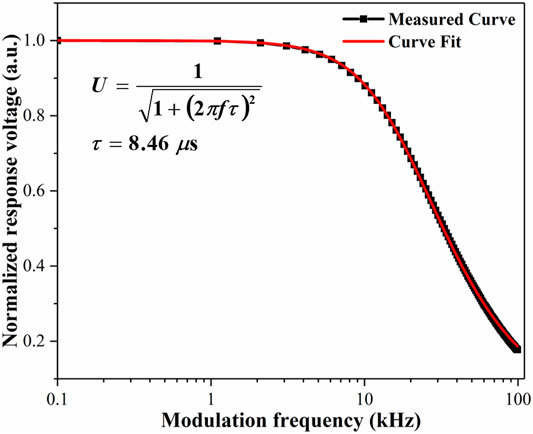
FIGURE 8. Normalized response voltage of the Nb5N6 microbolometer THz detector as a function of modulation frequency for the determination of the thermal time constant.
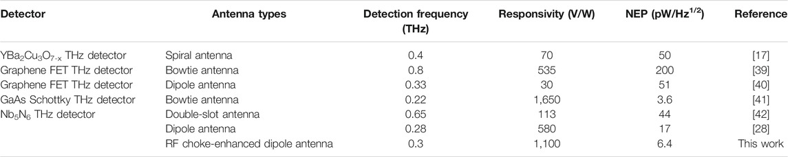
TABLE 1. Performance comparison between the proposed Nb5N6 THz detectors and other detectors.
The thermal time constant of the THz detector, which determines the speed of image processing, plays an important role in THz imaging technology. The shorter the response time, the faster the image acquisition speed. The measured normalized response voltage of the Nb5N6 THz detector as a function of modulation frequency is depicted in Figure 8. The normalized amplitude of the response voltage decreases with the increase of the modulation frequency. The measured data can be well fitted by the formula
To demonstrate the feasibility of the Nb5N6 THz detector in practical application, we applied it in a THz transmission imaging system. Figure 9 shows the schematic diagram of the transmission imaging system. A pair of off-axis parabolic mirrors is used to collimate and focus the modulated THz radiation, a two-dimensional displacement platform is used to move the object to realize the scanning, the THz radiation signals transmitted through the object are detected by the Nb5N6 THz detector, the final voltage signals are readout from a lock-in amplifier (SR830) to the computer, and the images of the objects are recovery from these measured raw data without image modification.
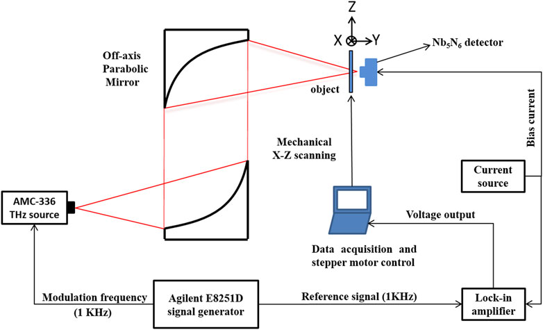
FIGURE 9. Schematic of the developed imaging system with the Nb5N6 THz detector at 0.308 THz.
Because of the low absorption of THz signals by plastics and the complete reflection of THz signals by metals, THz imaging technology is a very effective way for detecting metal or voids in solid plastic products and other objects containing different THz absorption coefficients. Two objects with different characteristics were used to achieve their images at 0.308 THz with the developed THz imaging system, as shown in Figure 10. The first object is a metal blade, and the THz radiation will fully pass through it or not depending on its shape, resulting in that the transmitted THz radiation at different position has nearly the unity intensity. Figure 10A shows the image of the blade; the red and the black parts represent the areas where the THz radiation can and not transmit, respectively. Details of the blade imaging, such as the edges and irregular holes, are extremely clear. The second object is an access card, whose components inside are more complicated than the blade, resulting in transmitted THz radiation at different part with different intensities. Figure 10B displays the image of the components hidden inside the access card, such as a coil and rectangular chip, which can be observed clearly. These results indicate that the performance of the Nb5N6 microbolometer THz detector integrated with RF choke-enhanced dipole antenna is good from another perspective and it is sufficient for practical applications.
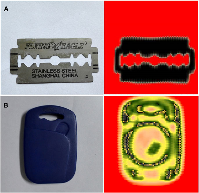
FIGURE 10. Photographs and THz images of a metal blade (A) and access card (B).
The Nb5N6 THz detector integrated with RF choke-enhanced dipole antenna was developed and demonstrated for 0.3 THz detection and imaging at room temperature. The simulated electric field intensity of the proposed RF choke-enhanced dipole antenna showed an improvement of 2.6 times compared to that without RF choke. The measured best optical responsivity of the Nb5N6 microbolometer THz detector integrated with the proposed antenna was 1100 V/W and the corresponding minimum NEP was 6.4 × 10⁻¹² W/Hz1/2 at 0.308 THz with 0.6 mA bias current. The response time of the Nb5N6 THz detector was as low as 8.46 μs. The measurement results were in good agreement with the simulation ones. Furthermore, a THz imaging system based on transmission mode was developed using the proposed detector, and the THz imaging of a blade and the access card was investigated. The results show that the obtained THz imaging has high resolution and a clear outline without any image processing. Especially, through the analysis of the transmission image of the access card, its internal structure could be clearly observed. It was demonstrated that the proposed antenna-coupled Nb5N6 THz detector had high sensitivity and fast response speed for THz imaging. The development of large-scale detector arrays for terahertz imaging using the proposed detector in this work is on the underway.
The original contributions presented in the study are included in the article/Supplementary Material; further inquiries can be directed to the corresponding authors.
CJ designed and simulated the structure. All authors analyzed and discussed the results. CJ and XT wrote the manuscript. The project was conceived and supervised by XT and LK.
This research was supported by the Key Technologies Research and Development Program (2018YFB1801504); National Natural Science Foundation of China (61521001 and 61801209); Fundamental Research Funds for the Central Universities; and Jiangsu Key Laboratory of Advanced Techniques for Manipulating Electromagnetic Waves.
The authors declare that the research was conducted in the absence of any commercial or financial relationships that could be construed as a potential conflict of interest.
All claims expressed in this article are solely those of the authors and do not necessarily represent those of their affiliated organizations, or those of the publisher, the editors, and the reviewers. Any product that may be evaluated in this article, or claim that may be made by its manufacturer, is not guaranteed or endorsed by the publisher.
1. Chan WL, Deibel J, Mittleman DM. Imaging with Terahertz Radiation. Rep Prog Phys (2007) 70(8):1325–79. doi:10.1088/0034-4885/70/8/R02
2. Siegel PH. Terahertz Technology in Biology and Medicine. IEEE Trans Microwave Theor Techn. (2004) 52(10):2438–47. doi:10.1109/TMTT.2004.835916
3. Yu C, Fan S, Sun Y, Pickwell-Macpherson E. The Potential of Terahertz Imaging for Cancer Diagnosis: A Review of Investigations to Date. Quant Imaging Med Surg (2012) 2(1):33–45. doi:10.3978/j.issn.2223-4292.2012.01.04
4. Ferguson B, Zhang X-C. Materials for Terahertz Science and Technology. Nat Mater (2002) 1(1):26–33. doi:10.1038/nmat708
5. Mittleman D. Sensing with Terahertz Radiation. Springer Berlin Heidelberg (2003). doi:10.1007/978-3-540-45601-8
6. Sizov F, Rogalski A. THz Detectors. Prog Quan Elect (2010) 34(5):278–347. doi:10.1016/j.pquantelec.2010.06.002
7. Golay MJE. A Pneumatic Infra‐Red Detector. Rev Scientific Instr (1947) 18(5):357–62. doi:10.1063/1.1740949
8. Siegel PH. Terahertz Technology. IEEE Trans Microwave Theor Techn. (2002) 50(30):910–28. doi:10.1109/22.989974
9. Knap W, Valusis G, Dyakonov M, Coquillat D, Teppe F, Lusakowski J, et al. Field Effect Transistors for Terahertz Detection: Physics and First Imaging Applications. J Infrared Millim Terahertz Waves (2009) 30(12):1319–37. doi:10.1007/s10762-009-9564-9
10. Miller AJ, Luukanen A, Grossman EN. Micromachined Antenna-Coupled Uncooled Microbolometers for Terahertz Imaging Arrays. Proc SPIE - Int Soc Opt Eng (2004) 5411:18–24. doi:10.1117/12.543236
11. Grant J, Escorcia-Carranza I, Li C, McCrindle IJH, Gough J, Cumming DRS. A Monolithic Resonant Terahertz Sensor Element Comprising a Metamaterial Absorber and Micro-bolometer. Laser Photon Rev (2013) 7(6):1043–8. doi:10.1002/lpor.201300087
12. Simoens F, Meilhan J. Terahertz Real-Time Imaging Uncooled Array Based on Antenna- and Cavity-Coupled Bolometers. Phil Trans R Soc A (2014) 372:20130111. doi:10.1098/rsta.2013.0111
13. Lee AWM, Wil BS, Kumar S, Qing Hu fnm, Reno JL. Real-time Imaging Using a 4.3-THz Quantum cascade Laser and a 320/spl Times/240 Microbolometer Focal-Plane Array. IEEE Photon Technol Lett (2006) 18(13):1415–7. doi:10.1109/LPT.2006.877220
14. Chen C, Yi X, Zhang J, Zhao X. Linear Uncooled Microbolometer Array Based on VOx Thin Films. Infrared Phys Tech (2001) 42(2):87–90. doi:10.1016/S1350-4495(01)00058-5
15. Pope T, Savchenko A, Thomas P, Hornsey R. Nonoptical Characterization Techniques for Uncooled Microbolometer Infrared Sensors. IEEE Trans Electron Devices (2000) 47(12):2294–300. doi:10.1109/16.887011
16. Cole BE, Higashi RE, Wood RA. Monolithic Two-Dimensional Arrays of Micromachined Microstructures for Infrared Applications. Proc IEEE (1998) 86(8):1679–86. doi:10.1109/5.704273
17. Bevilacqua S, Cherednichenko S. Low Noise Nanometer Scale Room-Temperature ${\hbox{YBa}}_{2}{\hbox{Cu}}_{3}{\Hbox{O}}_{7-x}$ Bolometers for THz Direct Detection. IEEE Trans Thz Sci Technol (2014) 4(6):653–60. doi:10.1109/TTHZ.2014.2344435
18. Almasri M, Butler DP, Celik-Butler Z. Self-supporting Uncooled Infrared Microbolometers with Low-thermal Mass. J Microelectromech Syst (2001) 10(3):469–76. doi:10.1109/84.946808
19. Shan PC, Çelik‐Butler Z, Butler DP, Jahanzeb A, Travers CM, Kula W, et al. Investigation of Semiconducting YBaCuO Thin Films: A New Room Temperature Bolometer. J Appl Phys (1996) 80(12):7118–23. doi:10.1063/1.363724
20. Qi L, Minkevičius L, Urbanowicz A, Švigelj A, Grigelionis I, Kašalynas I, et al. Antenna-Coupled Titanium Microbolometers: Application for Precise Control of Radiation Patterns in Terahertz Time-Domain Systems. Sensors (2021) 21(10):3510. doi:10.3390/s21103510
21. Monticone E, Boarino L, Lérondel G, Steni R, Amato G, Lacquaniti V. Properties of Metal Bolometers Fabricated on Porous Silicon. Appl Surf Sci (1999) 142(1):267–71. doi:10.1016/S0169-4332(98)00685-0
22. Jin-Shown Shie JS, Yeong-Maw Chen YM, Mang Ou-Yang fnm, Chou BCS. Characterization and Modeling of Metal-Film Microbolometer. J Microelectromech Syst (1996) 5(4):298–306. doi:10.1109/84.546409
23. Sedky S, Fiorini P, Caymax M, Loreti S, Baert K, Hermans L, et al. Structural and Mechanical Properties of Polycrystalline Silicon Germanium for Micromachining Applications. J Microelectromech Syst (1998) 7(4):365–72. doi:10.1109/84.735343
24. Sedky S, Fiorini P, Caymax M, Baert C, Hermans L, Mertens R. Characterization of Bolometers Based on Polycrystalline Silicon Germanium Alloys. IEEE Electron Device Lett (1998) 19(10):376–8. doi:10.1109/55.720191
25. Zimmers A, Aigouy L, Mortier M, Sharoni A, Wang S, West KG, et al. Role of Thermal Heating on the Voltage Induced Insulator-Metal Transition inVO2. Phys Rev Lett (2013) 110(5):056601. doi:10.1103/PhysRevLett.110.056601
26. Jagtap VS, Dégardin AF, Kreisler AJ. Low Temperature Amorphous Growth of Semiconducting Y-Ba-Cu-O Oxide Thin Films in View of Infrared Bolometric Detection. Thin Solid Films (2012) 520(14):4754–7. doi:10.1016/j.tsf.2011.10.127
27. Lu X, He N, Kang L, Chen J, Jin B, Wu P. Nb5N6 Thin Film on Silicon and Silicon Oxide: A Good Material for Terahertz Detection. Chin Sci Bull (2009) 54(18):3344–6. doi:10.1007/s11434-009-0485-8
28. Tu X-C, Kang L, Liu X-H, Mao Q-K, Wan C, Chen J, et al. Nb5N6microbolometer Arrays for Terahertz Detection. Chin Phys. B (2013) 22(4):040701. doi:10.1088/1674-1056/22/4/040701
29. Jiang Z, Men L, Wan C, Xiao P, Jiang C, Tu X, et al. Low-Noise Readout Integrated Circuit for Terahertz Array Detector. IEEE Trans Thz Sci Technol (2018) 8(3):350–6. doi:10.1109/TTHZ.2018.2819502
30. Lindberg P, Ojefors E. A Bandwidth Enhancement Technique for mobile Handset Antennas Using Wavetraps. IEEE Trans Antennas Propagat (2006) 54(8):2226–33. doi:10.1109/TAP.2006.879211
31. Wang Y-S, Lu J-C, Chung S-J. A Miniaturized Ground Edge Current Choke-Design, Measurement, and Applications. IEEE Trans Antennas Propagat (2009) 57(5):1360–6. doi:10.1109/TAP.2009.2016709
32. Noghanian S, Shafai L. Gain Enhancement of Annular Slot Antennas. IEE Proc Microw Antennas Propag (2001) 148(2):109–14. doi:10.1049/ip-map:20010331
33. Kishk AA, Shafai L, Ittipiboon A. Improvement in Radiation Characteristics of Coaxial Feeds Using a Quarter-Wavelength Choke. Electron Lett (1984) 20(12):522–3. doi:10.1049/el:19840362
34. Szakmany GP, Orlov AO, Bernstein GH, Porod W. Response Increase of Antenna-Coupled Nanothermocouples by thermal Insulation. J Vacuum Sci Tech B (2018) 36(5):052203. doi:10.1116/1.5044534
35. Coquillat D, Marczewski J, Kopyt P, Dyakonova N, Giffard B, Knap W. Improvement of Terahertz Field Effect Transistor Detectors by Substrate Thinning and Radiation Losses Reduction. Opt Express (2016) 24(1):272–81. doi:10.1364/OE.24.000272
36. Hosotani T, Kasuya F, Taniguchi H, Watanabe T, Suemitsu T, Otsuji T, Ishibashi T. Lens-integrated Asymmetric-Dual-Grating-Gate High-Electron-Mobility-Transistor for Plasmonic Terahertz Detection. In: 2017 IEEE MTT-S International Microwave Symposium (IMS); 4-9 June 2017; Honololu, HI, USA. IEEE (2017). p. 578–81. doi:10.1109/MWSYM.2017.8058632
37. Ali M, Perenzoni M, Stoppa D. A Measurement Setup for THz Detectors Characterization Validated on FET-Based CMOS Test Structures. In: Conference Record - IEEE Instrumentation and Measurement Technology Conference, 2015; 11-14 May 2015; Pisa, Italy. IEEE (2015). p. 320–4. doi:10.1109/I2MTC.2015.7151287
38. Ojefors E, Pfeiffer UR, Lisauskas A, Roskos HG. A 0.65 THz Focal-Plane Array in a Quarter-Micron CMOS Process Technology. IEEE J Solid-state Circuits (2009) 44(7):1968–76. doi:10.1109/JSSC.2009.2021911
39. G K RM, Deshmukh P, Prabhu SS, Basu PK. Antenna Coupled Graphene-FET as Ultra-sensitive Room Temperature Broadband THz Detector. AIP Adv (2018) 8(12):125122. doi:10.1063/1.5063399
40. Qin H, Sun J, Liang S, Li X, Yang X, He Z, et al. Room-temperature, Low-Impedance and High-Sensitivity Terahertz Direct Detector Based on Bilayer Graphene Field-Effect Transistor. Carbon (2017) 116:760–5. doi:10.1016/j.carbon.2017.02.037
41. Qiao HD, Liu H, Mou JC, Lv X. 220 GHz Focal Plane Imaging Demonstration Using Integrated Terahertz Array Detector. Microw Opt Technol Lett (2020) 62(9):2826–9. doi:10.1002/mop.32388
Keywords: Nb5N6 microbolometer, THz detector, RF choke, antenna, THz imaging
Citation: Jiang C, Tu X, Wan C, Kang L, Jia X, Chen J and Wu P (2021) High-Sensitivity RF Choke-Enhanced Dipole Antenna-Coupled Nb5N6 THz Detector. Front. Phys. 9:768192. doi: 10.3389/fphy.2021.768192
Received: 31 August 2021; Accepted: 27 September 2021;
Published: 03 November 2021.
Edited by:
Meng Chen, Tsinghua University, ChinaReviewed by:
Mingyu Zhang, Harbin Institute of Technology, Shenzhen, ChinaCopyright © 2021 Jiang, Tu, Wan, Kang, Jia, Chen and Wu. This is an open-access article distributed under the terms of the Creative Commons Attribution License (CC BY). The use, distribution or reproduction in other forums is permitted, provided the original author(s) and the copyright owner(s) are credited and that the original publication in this journal is cited, in accordance with accepted academic practice. No use, distribution or reproduction is permitted which does not comply with these terms.
*Correspondence: Xuecou Tu, tuxuecou@nju.edu.cn; Lin Kang, kanglin@nju.edu.cn
Disclaimer: All claims expressed in this article are solely those of the authors and do not necessarily represent those of their affiliated organizations, or those of the publisher, the editors and the reviewers. Any product that may be evaluated in this article or claim that may be made by its manufacturer is not guaranteed or endorsed by the publisher.
Research integrity at Frontiers
Learn more about the work of our research integrity team to safeguard the quality of each article we publish.