 Joel Minguet Lopez*Sylvain BarraudDavid CooperAudrey JannaudAdeline GrenierAurelie SouhaitéJean-Michel PediniCorinne ComboroureAhmed GharbiFrançois BoulardClément CastanAmélie LambertFrançois Andrieu
- University Grenoble Alpes, CEA-Leti, Grenoble, France
Neural Network hardware in-memory implementations based on memristive synapses are a promising path towards energy efficient Edge computing. Among others, Oxide-based Resistive Random Access Memory (OxRAMs) devices utilization for synaptic weight hardware implementation has shown promising performance on various types of Neural Networks, notably when coupled with bit-error correcting codes or adaptive programming schemes for the device intrinsic variability management. In this context, memristive footprint reduction coupling with Multi-Level-Cell (MLC) operation remains essential to hardware implement highly accurate state-of-art Neural Networks, whose number of parameters is exponentially increasing over time. In this work, a compact OxRAM-based 1 Transistor – 1 Resistor (1T1R) architecture, where the memory is integrated inside the 40 nm × 40 nm drain contact of thin-gate oxide FDSOI transistors, is demonstrated in 28 nm technology. The memory structure is optimized from the OxRAM active material level to the cell architecture. This results in 106 endurance and 11-level MLC encoding resilient to 109 inference cycles compatible with 0.0357 μm2 bitcell footprint potential in 28 nm technology. Altogether, the proposed 1T1R cell density is competitive with respect to ultra-dense 1S1R-based Crossbar arrays, while being compatible with in-memory Neural Network inference implementations on-chip.
1 Introduction
Recent progress on deep learning accelerators enabled impressive performance on a wide range of applications. However, deep learning accelerators consume enormous amount of energy when accelerated in both graphics processing units (GPU) and central processing units (CPU) platforms, which remains extremely limiting in the distributed intelligence Internet of Things paradigm. Indeed, the vast majority of this energy consumption is not associated to the computation itself but to data movement between both the arithmetic and storage blocks, which are physically distant in GPUs and CPUs. Particularly, this represents a big challenge for state-of-art Artificial Neural Networks (ANNs) hardware implementation with very large number of parameters, which require a very large amount of memory accesses and operations. In this context, developing non-von Neumann computing architectures enhancing close co-integration of logic and memorization is crucial to optimize the overall capabilities of current electronic hardware, moving towards in or near-memory computing with very few data movement within the system (Sze, 2019).
In particular, ANN’s inference rely on the Multiply-and-accumulate (MAC) operation between activation inputs and synaptic weights. Notably, the implementation of this operation using Non-Volatile Memory (NVM) based memristive arrays, where the synapses are analogically represented by the memory devices, has demonstrated remarkable energy efficiency (Xue et al., 2019) capabilities in comparison with other alternative approaches (Murmann, 2021). Nevertheless, these approaches remain very demanding for the memristive devices used for the synapses hardware implementation. Among others, two main requirements are crucial. First, developing very dense memory architectures able to scale towards big memory capacities on-chip is essential to sustain the exponential increase through time of the total number of parameters in state-of-art Neural Networks. This allows limiting unnecessary array partitioning to perform the computation and therefore simplifying the routing peripherals dimensioning on-chip, and preserving overall reasonable silicon footprint. Second, developing memristor technologies with Multi-Level Cell (MLC) capabilities remains key to implement state-of-art Neural Networks with high accuracy, which require high precision leveraged for their parameters representation (Aguirre et al., 2024; Nagel et al., 2021). In addition, ensuring the stability of the programmed states on the MLC memristive cells to reading pulses remains critical in the context of inference computing, which requires applying huge amounts of repeated reading operations in the memristors.
Globally, it remains extremely challenging to develop such a polyvalent memory technology (Molas and Nowak, 2021). Among others, metal oxide resistive memory (OxRAM) is a promising candidate for Neural Network synaptic weight hardware implementation (Wan et al., 2022), especially when operated using bit-error correcting codes or adaptive programming schemes (Jain et al., 2019; Chou et al., 2020) to counterbalance their intrinsic resistance fluctuations due to conductive filament relaxation effects (Reganaz et al., 2023). However, ensuring OxRAM-based memristive solutions scalability towards very dense architectures compatible with advanced technology nodes remains challenging. 1S1R-based Crossbar architectures represent the state-of-the-art in terms of memory density at the moment, as they promise 4F2 memory bitcell potential (Kau et al., 2009) (where F is the minimal dimension which can be obtained by photolithography in a given technological node). However, 1S1R-based Crossbar technology does not allow the in-memory MAC analog implementation when operated in MLC mode, which represents an important obstacle for its utilization as technological platform for in-memory NN deployment on-chip. Alternatively, the on-chip co-integration between resistive memory devices and advanced logic transistors has been recently proposed for 1T1R architectures densification (Shen et al., 2012; Wu et al., 2020; Shulaker et al., 2014; Dubreuil et al., 2023a; Li et al., 2016; Xie et al., 2023, Minguet Lopez et al., 2025). Nevertheless, elucidating the impact of the memory stack and the cell routing protocols on their scalability towards high capacity memory arrays able to perform in-situ logic computations remains essential.
In this work, we propose to rethink the standard 1 Transistor – 1 Resistor (1T1R) cell to achieve competitiveness with the density of 1S1R crossbar architectures (Figure 1). To do so, we fabricate and deeply characterize a 3D monolithic 1T1R cell, which is based on the HfO2-based OxRAM deposition inside the 28 nm FDSOI CMOS transistor drain contact. We carry out a theoretical and experimental study to evaluate the cell dimensional scalability and its compatibility with advanced technological nodes, by coupling cell architectural optimization with specific device operating protocols and stack optimization based on Si implantation. Based on this analysis, guidelines for an improved device reliability, reduced cell footprint and enhanced compatibility with advanced node technologies are provided. Overall, the pertinence of our approach as memristive solution for Neural Network inference hardware implementations at the Edge is demonstrated, benefiting from analog MLC MAC direct implementation in the memory array with state-of-art 0.0357 μm2 cell footprint.
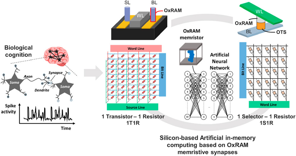
Figure 1. In this work we focus on in-memory implementations using memristive synapses of Artificial Neural Network, which promise neurons and synapses co-location similarly to biological cognitive structures. Taking into consideration OxRAM memristors, this work aims to optimize 1 Transistor – 1 Resistor (1T1R) structures performance in the context of Neural Network on-chip inference implementations. The ultra-dense 1 Selector – 1 Resistor (1S1R) Crossbar arrays are taken as a reference.
Partial and preliminary results of the devices characterized in this work were presented in (Minguet Lopez et al., 2025). This paper provides additional electrical measurements, enlarging from two to seven the number of OxRAM stacks which are electrically characterized and exploring the device forming, SET and RESET programming reliability in more depth. Moreover, this paper provides nanoscale characterization based on STEM-EELS and STEM-EDX techniques on memory devices which have been formed with negative biases, aiming to fully elucidate the operating possibilities of our OxRAM cells and the programming impact on the different material stack layers. Finally, this paper provides a detailed comparison between the proposed 3D monolithic 1T1R cell and ultra-dense Crossbar structures in the context of Neural Network on-chip inference implementations.
2 Background
2.1 Intrinsic limitations of Multi-Level Cell 1S1R-based crossbar structures for analog MAC implementations in-memory
The replacement of the standard 1 Transistor – 1 Resistor (1T1R) memory architecture by 1 Selector – 1 Resistor (1S1R) Crossbar memory structures based on Ovonic Threshold Switch (OTS) selector co-integration with non-volatile resistive memory devices has been proposed for both phase-change (Kau et al., 2009; Bourgeois et al., 2023; Lepri et al., 2023) and OxRAM (Minguet Lopez et al., 2024, 2021) memory devices. Remarkably, Crossbar architectures allow a potential memory bitcell shrink down to 4F2, where F is the minimal dimension which can be obtained by photolithography in a given technological node, and therefore are very promising to achieve very dense memristive systems. In these structures, the higher the resistance programmed in the memory device and the higher the resulting 1S1R switching voltages (Vth) due to the additional voltage drop on the memory. Therefore, taking an OxRAM-based 1S1R Crossbar into account, the ability to program N distinct resistive states on the OxRAM device results into the definition of N distinct 1S1R switching voltages (Vth,1, Vth,2, … Vth,n) (Figure 2). Moreover, the read operation of a 1S1R device with N distinct 1S1R switching voltages relies on the application of (N-1) reading voltages (Figure 3). When operated over threshold, the current crossing the 1S1R stack during the read operation can only take two values. ION crosses the stack when the OTS selector switches during the reading pulse and Ith<<ION crosses the stack when the OTS selector does not switch during the reading pulse. Accordingly, the resulting current crossing the 1S1R stack is not proportional to the resistance value encoded in the OxRAM device, impeding the implementation of an in-memory analog MAC based on Ohm’s and Kirchoff’s law. In addition, projecting towards near-memory MAC implementations, both the 1S1R-based MLC MAC latency and energy consumption are strongly degraded due to the need for multiple reading operations in the device. This represents an important blocking factor for near-memory MAC implementations with 1S1R-based Crossbar structures. Finally, both the OxRAM and OTS intrinsic variability strongly impact the 1S1R MLC feasibility (Minguet Lopez et al., 2021), limiting the total number of resistive levels that can be encoded in the device without overlapping. Notably, up to only 3 levels encoding at the cell level has been demonstrated in the literature without statistical overlapping through cycling (Minguet Lopez et al., 2024).
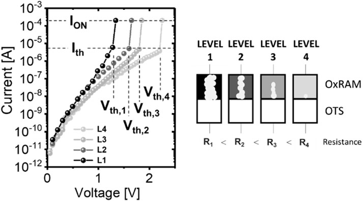
Figure 2. 1S1R 4-level Multi-Level Cell experimental current-voltage characteristics, where four resistive levels (R1, R2, R3, R4) are programmed in the OxRAM device. Adapted from Minguet Lopez et al. (2024).
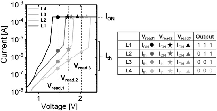
Figure 3. 1S1R Multi-Level Cell reading protocol description, where four resistive levels (R1, R2, R3, R4) are programmed in the OxRAM device (Minguet Lopez et al., 2024). The definition of N resistance levels in the OxRAM device result into N distinct 1S1R switching voltages. In order to identify the OxRAM resistive state, the application of (N-1) reading voltages is required (Minguet Lopez et al., 2024).
Overall, despite 1S1R-based Crossbar architectures allow very dense 4F2 bitcell potential, their pertinence as technological platform for in or near-memory analog Neural Network acceleration remains strongly limited by the 1S1R device intrinsic properties.
2.2 Analog MAC implementation in-memory with 1T1R memristive cells
Therefore, adopting 1T1R single memristor arrays as technological platform for in-memory analog Neural Network acceleration remains of big interest, as they naturally allow the in-memory implementation of MAC operations relying on Ohm’s and Kirchoff’s current law. However, there is no consensus on the ability of OxRAM-based 1T1R memory cells to shrink and give birth to very dense memory arrays while being compatible with advanced technological nodes. In particular, OxRAM-based 1T1R memory arrays scalability towards dense structures may be strongly limited by various factors. First, the OxRAM device operating currents and voltages strongly impact the resulting 1T1R cell footprint, as they are a determining factor of the selection transistor dimensioning and so its active area dimensions. In particular, this trend is mostly associated to the OxRAM high forming voltages required for device initialization, as well as the device SET and RESET currents (Sandrini et al., 2019). Second, the 1T1R cell footprint can be impacted by the memory device position in the metal stack and the associated routing strategy in a given technological node. Third, the 1T1R cell footprint can directly be impacted by the OxRAM resistor (1R) size. This trend can be particularly impactful when projecting towards very advanced technological nodes with very aggressive metal pitch dimensions, where the metal pitch shrink must be accompanied by a reduced OxRAM resistor (1R) section and pitch. These dependences are illustrated in Figure 4, comparing the 1T1R bitcell size and the corresponding 1R OxRAM size evolution with the selecting transistor technological node for various industrial macros (Huang et al., 2024; Golonzka et al., 2019; Hayakawa et al., 2015; Ito et al., 2018, Chang et al., 2014, Xue et al., 2019). When moving towards advanced technological nodes, it becomes important to achieve OxRAM functionality at shrink memory sizes with limited operating voltages and currents to sustain the overall 1T1R cell area reduction with the transistor generations.
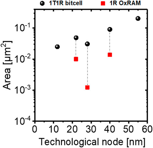
Figure 4. OxRAM-based 1T1R bitcell scalability as a function of the selecting transistor technological node. The corresponding OxRAM 1R sizes are provided when available in the literature (Huang et al., 2024; Golonzka et al., 2019; Hayakawa et al., 2015; Ito et al., 2018, Chang et al., 2014, Xue et al., 2019).
3 Sample and methods description
In order to provide a response to these challenges, we propose to rethink the OxRAM-based 1T1R cell architecture and stack characteristics, moving towards a memory-transistor co-location near the FEOL. Figure 5A summarizes our process integration approach in 300 mm platform (Minguet Lopez et al., 2025). A separate MEOL drain and source contact opening is required in our integration flow, which imposes a single extra lithography mask in comparison with a standard 300 mm 28 nm FDSOI CMOS process flow (Planes et al., 2012). Then, the HfO2-based OxRAM stack is deposited inside the drain contact. The stack consists on a 5 nm-thick HfO2 layer deposited by Atomic Layer Deposition (ALD) and a Ti (RFPVD)/TiN (CVD) top electrode, which are directly deposited on NiPtSi Silicide (acting as bottom electrode). Various alternative bottom electrode approaches exist, notably the utilization of Si-doped bottom electrodes (Dubreuil et al., 2023b). Nevertheless, NiPtSi silicide allows achieving low-resistance contacts, good thermal stability and good compatibility with the specific requirements of FDSOI transistors, making it pertinent for our compact 1T1R cell. The main goal being to enlarge the OxRAM window margin (to maximize its MLC capabilities) while preserving bitcell scalability, various OxRAM active materials are studied: standard HfO2 and four different flavors with Si implantation into HfO2 (“S1,” “S2,” “S3,” “S4”). An increasing number identification corresponds to a higher Si concentration in the active material. In addition, 4nm and 5 nm thick OxRAM layers are considered in the analysis. After OxRAM deposition, the filling of the W-based bitline pillar gives rise to the BEOL metallization. 0.0016–0.0032 μm2 contact sizes are considered, leading to two distinct OxRAM (1R) sizes. Figure 5B (resp. Figure 5C) provide TEM and EDX cross-section of source (resp. drain) contacts on our compact structure straight after fabrication. A consistent co-integration of all layers during the fabrication process is demonstrated.
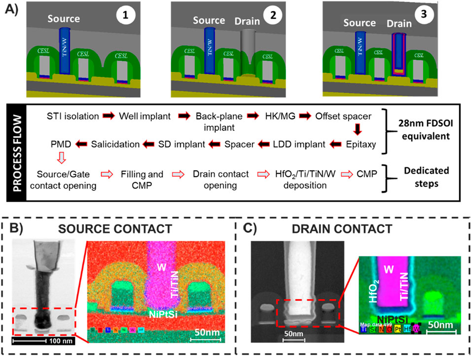
Figure 5. (A) Illustrative integration process used to fabricate our compact OxRAM-based 1T1R memory cell, together with the dedicated process flow (Minguet Lopez et al., 2025). (B) Source contact EDX and TEM images. (C) Drain contact EDX and TEM images, illustrating the satisfactory OxRAM deposition.
4 Experimental results
4.1 OxRAM stack optimization for low forming voltages and reliable memristor operation
As introduced previously, the OxRAM forming voltages remain one of the main factors limiting overall 1T1R cell scalability. In this context, it has been proven that the OxRAM layer thickness play a key role on the resulting forming voltages (Govoreanu et al., 2011). Figure 6A illustrates our OxRAM pristine resistance evolution as a function of the device stack. Both OxRAM thickness and composition engineering with Si implantation approaches are considered. In addition, Figure 6B illustrates the correlation between the device pristine resistance Rpristine and its forming voltages Vforming. In this analysis, positive forming voltages are applied to the OxRAM top electrode. The application of several forming pulses with progressive voltage amplitude increase is considered to initialize the cells. After the application of each forming pulse, the cell resistance is read and compared to a predefined LRS resistance threshold. While the cell resistance does not reach the LRS target resistance, a subsequent pulse with a higher positively-biased voltage is applied. When the cell resistance reaches the target LRS resistance, the cell is considered as formed and the application of forming electrical pulses stops (Figure 6C). Remarkably, both HfO2 thickness reduction and increased implanted Si concentration allows reducing the device pristine resistance (Figure 6A), which translates into the reduction of its forming voltages (Figure 6B). This trends are in agreement with our OxRAM standard BEOL device (Grenouillet et al., 2021).
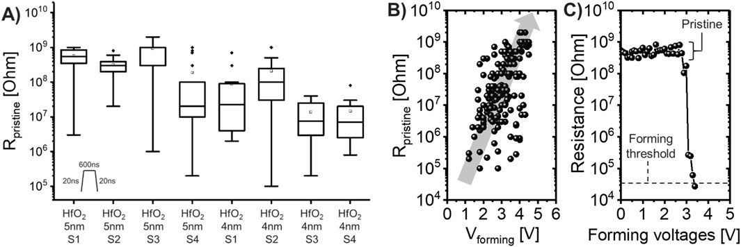
Figure 6. (A) Experimental OxRAM pristine resistance evolution with the stack characteristics, taking into account both HfO2 thickness and dose of Si implantation. 0.0032 μm2 contact sizes are taken into account. (B) Experimental OxRAM pristine resistance correlation with the device forming voltages, considering the same pulse characteristics. Again, 0.0032 μm2 contact sizes are taken into account. The provided positive forming voltages are applied to the OxRAM top electrode. (C) Illustrative OxRAM resistance evolution with the application of 600 ns length positive forming voltages in the device top electrode. Cells are considered to be formed when reaching a predefined LRS resistance value (forming threshold). Engineering the compliance current used during the forming process allows modulating the resistance obtained in the OxRAM cells after the forming operation.
However, ensuring reliable device operation once the forming process is done remains essential. Particularly, it remains key to guarantee large read window margin to maximize MLC capabilities, while maximizing the device endurance. Figure 7 provides multiple OxRAM endurance characteristics for some of the stacks of interest (Figure 7A), together with the electrical conditions used to program the cells (Figure 7B). While remaining at similar endurance capabilities, the progressive increase of the overall Si concentration in the OxRAM active material induces a progressive reduction of the resulting device window margin RHRS/RLRS, due to a HRS resistance decrease. As an illustration, it can be observed that the 5 nm-thick HfO2 S4 stack promises lower mean window margin than non-implanted 5 nm-thick HfO2 stack at parity of endurance capabilities. Likewise, 4 nm-thick HfO2 S1 promises lower mean window margin than 5 nm-thick HfO2 S1 at parity of endurance capabilities. In return, the progressive increase of the overall Si concentration in the OxRAM active material allows reducing the device programming voltages, synonym of lower programming energy consumption. Aiming to better understand the origin of this trend, Figure 8A provides the dependence between the OxRAM device forming voltages and the subsequent endurance capabilities on the device. The reported endurance corresponds to the number of applied programming cycles inducing the non-reversible degradation of the device window margin. No clear tradeoff is observed between the two, suggesting the absence of strong degradation on the device during the forming operation. Moreover, Figure 8B characterizes the device mean window margin evolution with its endurance capabilities, suggesting the existence of a tradeoff between the two. Each point corresponds to a single endurance cycling characterization, where the reported endurance (x-axis) corresponds to the number of applied programming cycles inducing the non-reversible degradation of the device window margin. The corresponding mean window margin is then calculated taking into account the applied programming cycles until endurance limit. Various programming conditions are used to characterize this tradeoff, focusing on both the SET and RESET voltages and its respective pulse lengths modulation. Each point representing a 1T1R cell endurance characterization, Figure 8C statistically illustrates the impact of some programming conditions to the resulting mean window margin in the cells. It worth noting the importance of balancing the SET and RESET pulse characteristics. First of all, avoiding the application of excessive SET or RESET voltages remains key not to degrade the device mean window margin. For example, coupling positive >2.2 V SET with negative >1.4 V RESET is observed to induce a mean window margin degradation on Si-implanted stacks, degradation which could be weighted by the pulse duration. Then, while guaranteeing SET operation effectiveness, balancing the negative RESET voltages to ensure sufficient but not excessive impact on the cells remains necessary. On one hand, it seems necessary to guarantee >1 V RESET negative voltages on Si-implanted stacks to give rise to a non-null mean window margin, while applying >1.8 V positive SET voltages. On the other hand, a larger mean window margin is observed on Si-implanted stacks when enlarging the RESET voltages up to −1.2 V, while applying >1.8 V positive SET voltages. This trend is notably observed on the non Si-implanted HfO2 stack, showing a larger mean window margin when increasing the RESET voltages up to −2.2 V while keeping similar SET conditions.
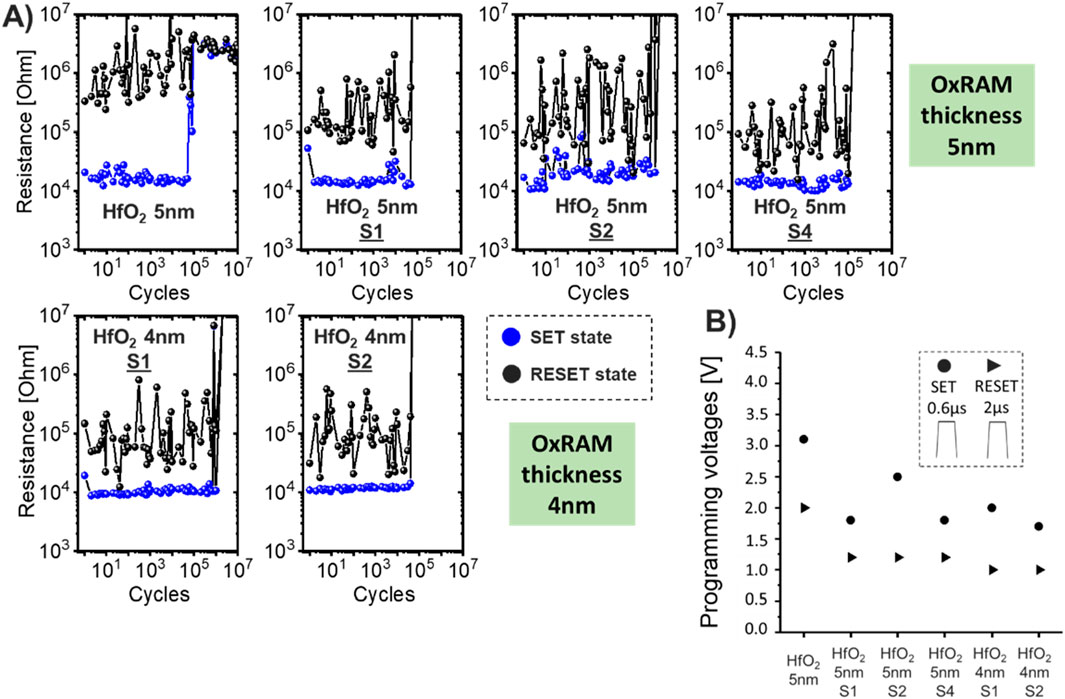
Figure 7. (A) Experimental OxRAM endurance capabilities, considering various 0.0032 μm2 OxRAM flavors. (B) Programming voltages used to obtain the endurance characteristics provided in (A). 0.6 µs (resp. 2 µs) SET (resp. RESET) pulses are used for the analysis. The absolute value of the negatively biased RESET voltages is provided. The SET compliance currents are kept constant while no current limitation is imposed during the RESET operation.
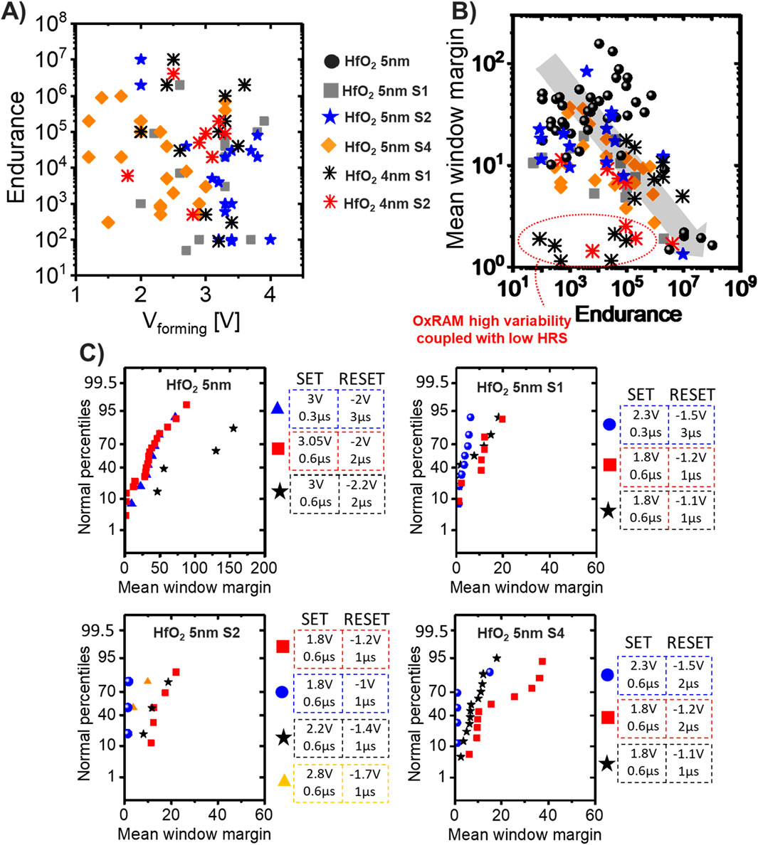
Figure 8. (A) OxRAM-based 1T1R endurance dependence with the initial forming voltages required for device initialization. Various stacks are initialized at positive bias with 600ns pulses. (B) Illustration of the tradeoff between the OxRAM mean window margin and its endurance capabilities, taking into consideration endurance characterization over 126 1T1R cells. 0.0032 μm2 contact sizes are taken into account. (C) OxRAM programming conditions impact on the resulting device mean window margin, taking various stacks in consideration. Each point corresponds to an endurance characterization. The same compliance current is imposed to the devices during SET operation.
Altogether, even if the 5 nm-thick non-implanted HfO2 stacks promise the larger mean window margin values, this comes at the expense of higher forming and operating voltages. Unfortunately, this remains an important blocking point for their utilization as memristive device when projecting towards advanced technological nodes.
Moreover, Figures 9, 10 aim to generalize those trends to OxRAM cells formed in the negative voltage bias domain, wishing to fully elucidate the operating possibilities of our memory cells. In particular, we propose to study the OxRAM cells functionality while being formed with the application of negative voltages in the stack top electrode, resulting into the NiPtSi bottom electrode acting as gettering electrode as suggested by (Chen et al., 2012; Wu et al., 2015; Raghavan et al., 2011). Standard 5 nm-thick HfO2 OxRAM stacks without Si implantation are considered in the analysis.
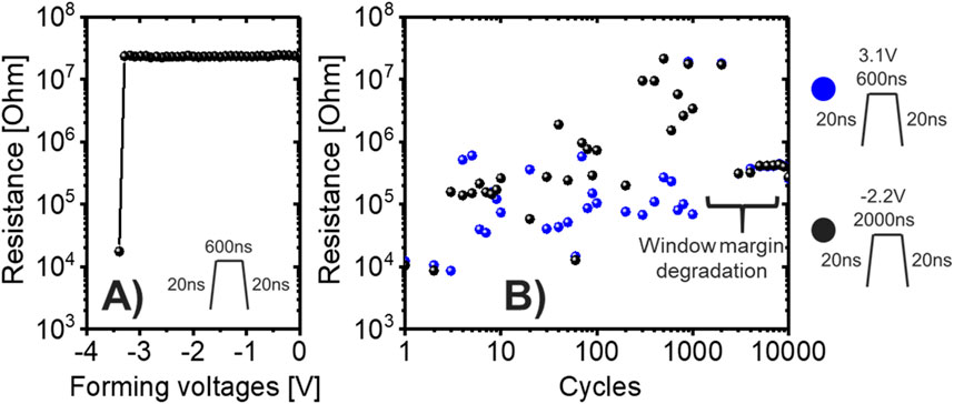
Figure 9. (A) Standard 5 nm-thick HfO2 OxRAM resistance evolution with the application of negative forming voltages in the top electrode, demonstrating the ability to initialize the cells in the negative bias regime. (B) Standard 5 nm-thick HfO2 OxRAM endurance characteristics after a forming operation in the negative bias regime. The device formed at (A) is taken into consideration.
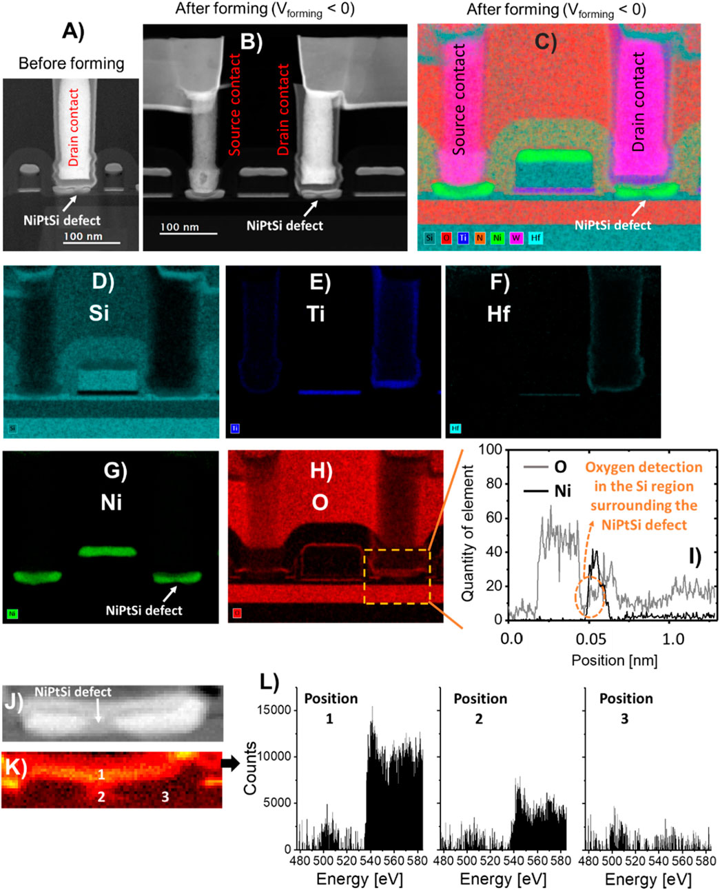
Figure 10. (A) Drain contact TEM image before OxRAM device forming process. A standard 5 nm-thick HfO2 OxRAM cell without Si implantation is considered. (B) OxRAM-based 1T1R cell TEM cross-section after forming process realization in the negative bias regime, taking into consideration a different OxRAM cell with the same stack characteristics. (C) OxRAM-based 1T1R cell EDX cross-section after forming process realization in the negative bias regime, considering the same cell as (B). (D–H) OxRAM-based 1T1R cell EDX cross-section after forming process realization in the negative bias regime, focusing on Si, Ti, Hf, Ni and O elements. The analysis concerns the cell studied in (B). (I) O and Ni elementary tracking in around the OxRAM stack of interest. Oxygen is again detected in the Si region Si region surrounding the NiPtSi bottom electrode defect. (J, K) Drain contact EELS spectrum image and the corresponding Oxygen elementary map. (L) Oxygen K-edge EEL spectra performed on the negatively formed OxRAM device in (B), focusing on three different positions around the NiPtSi bottom electrode defect zone indicated in (K). Oxygen is detected in the Si region surrounding the NiPtSi bottom electrode defect (position 2).
The OxRAM resistance evolution with the application of negatively biased 600ns forming pulses in the device top electrode is illustrated in Figure 9A, satisfactorily demonstrating the ability to initialize the devices in the negative bias regime. In addition, Figure 9B provides the subsequent OxRAM endurance experimental characteristics after a forming operation in the negative bias regime. Even if the application of adapted bipolar SET and RESET pulses allows obtaining a read window margin, the cell reliability through cycling after negative forming operation remains very limited. In particular, the mean window margin appears to be degraded due to fluctuating SET and RESET programmed resistance values and the overall endurance capabilities remain very limited. Aiming to better understand the origin of this trend, Figure 10A provides a TEM image on the OxRAM stack of interest, before the initial forming operation. In addition, Figures 10B, C provide the equivalent analysis after the application of an aggressive negative forming operation on an OxRAM cell with the same stack characteristics, focusing on both TEM and EDX cross-sections. It worth noting the presence of minor defects in the NiPtSi bottom electrode on both scenarios, suggesting their apparition during the device fabrication process. Then, Figures 10D–H provide specific elementary EDX cross-sections for the 5 nm-thick HfO2 cell of interest (Figures 10B, C), taking into consideration Si, Ti, Hf, Ni and O elements. Notably, the consistent integration of the OxRAM top electrode (Figure 10E) and the HfO2-based active layer is demonstrated (Figure 10F), guaranteeing no impact of the bottom electrode irregularities on the rest of the memory stack. This supports the satisfactory OxRAM operating reliability when formed in the positive regime (Figure 7), as the Ti/TiN top electrode is exploited as gettering layer. However, this is no longer valid when implicating of the NiPtSi bottom electrode as gettering layer by adopting negative forming voltages, which induces an initial Oxygen diffusion towards the stack bottom electrode. Figure 10I illustrates O and Ni elementary tracking in around the OxRAM stack based on Figure 10H EDX cross-section. In addition, Figure10L provides Oxygen K-edge EEL spectra performed on three different positions (Figure 10J, K) around the OxRAM NiPtSi bottom electrode. During the aggressive negative forming operation, the presence of defects in the bottom electrode unfortunately allows Oxygen diffusion into the Si region surrounding the NiPtSi defect (Figure 10I, L), resulting into the apparition of Si-O bonds as suggested by (Raghavan et al., 2011). Oxygen atoms implicated on Si-O bonds being no longer mobile when applying subsequent electrical pulses to the stack, this contributes to the device capabilities degradation when adopting negatively biased forming strategy (Figure 9).
Overall, negatively formed OxRAM cells suffer from a very limited operating reliability, blocking their exploitation as memristive device solution.
Although optimizing the mean window margin gives valuable information about the device performance during its lifetime, it does not allow to elucidate the origin and quantize the occurrence of reversible “soft” bit errors on the device during cycling. To this purpose, Figure 11A illustrates the OxRAM programmed resistance (ROxRAM) dependence with the IOxRAM current crossing the device during the programming pulse. While IOxRAM is measured during the programming pulse, ROxRAM is measured afterwards thanks to the application of a low voltage reading pulse. In other words, short-term relaxation phenomena can take place in the device in between the IOxRAM and ROxRAM measurements. IOxRAM current being a marker of the device active region morphological state during the applied programming pulse at such shrink OxRAM sizes, evaluating the OxRAM programmed resistance variability for various IOxRAM current ranges (Figure 11B) allows characterizing the device resistive stability. {5 nm-thick HfO2 S1, 5 nm-thick HfO2 S4, 4 nm-thick HfO2 S1, 4 nm-thick HfO2 S2} OxRAM stacks, identified as the most promising in the previous analysis, are studied in the analysis. Endurance experiments on various cells with 600ns programming pulses are taken into consideration. No significant difference is observed between the different OxRAM stacks at low resistance values, which is a signature of the presence of big and stable filaments in the device at this resistance regime. However, the stacks behave differently for intermediate and high programmed resistive states, where both the residual filament and the bulk contribution play a role on the resulting device resistance. ∼107 Ω high resistances appear to be reachable with 5 nm thick stacks, while 4 nm thick stacks peak at ∼106 Ω resistances despite RESET voltages increase. Unfortunately, this results into degraded mean window margin values on 4 nm thick stacks (Figure 7C), due to the existence of OxRAM high variability issues coupled with a reduced HRS value. Globally, this represents a strong blocking point for 4 nm thick stacks utilization as memristive device.
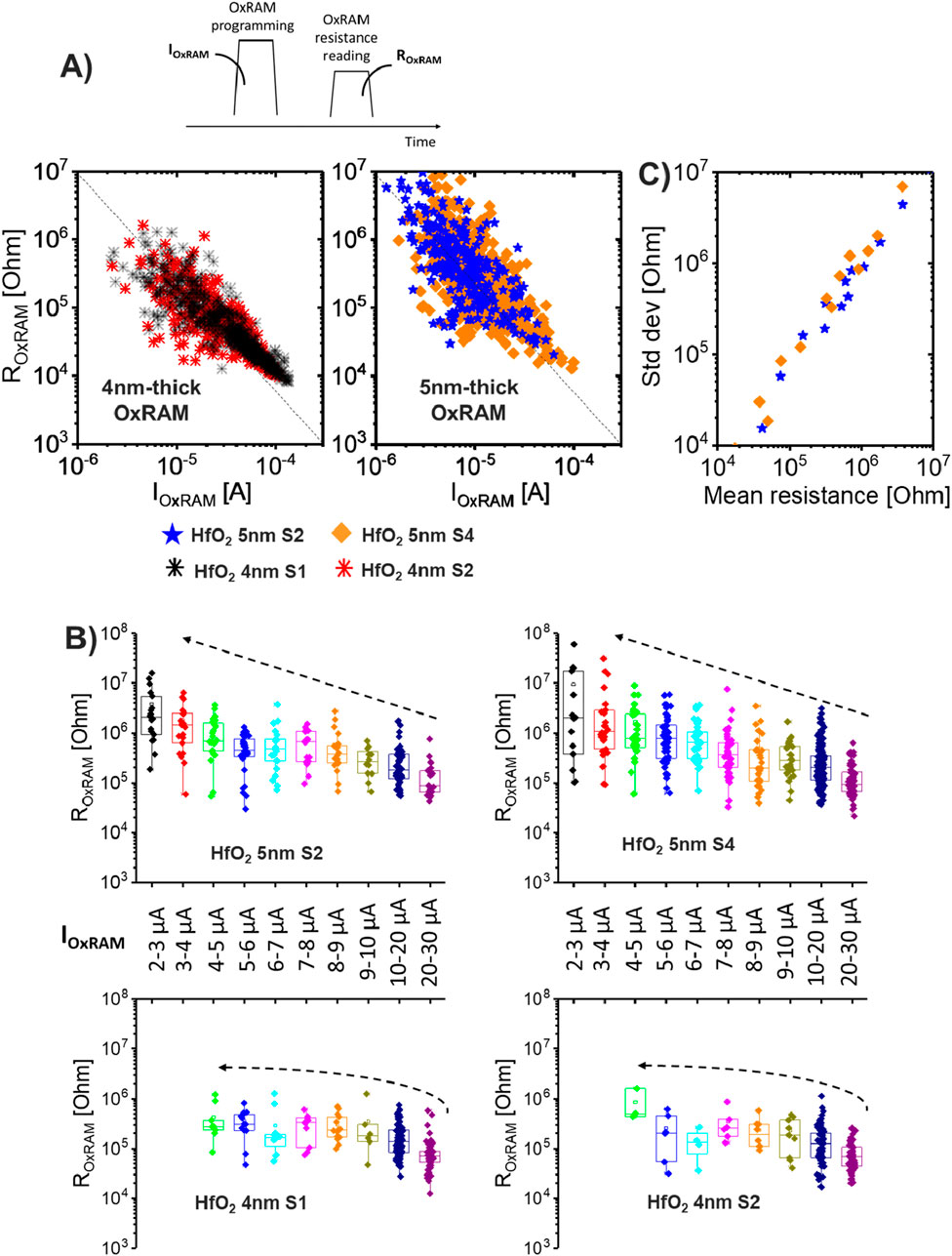
Figure 11. (A) Experimental OxRAM programmed resistance evolution with the current crossing the device during RESET operation (IOxRAM), taking into consideration four distinct states. 0.0032 μm2 contact sizes are taken into account. (B) Experimental OxRAM programmed resistance distributed over various IOxRAM current ranges. 0.0032 μm2 contact sizes are taken into account. (C) Standard deviation evolution with the mean resistance value for each IOxRAM current range, taking into consideration various stacks.
Overall, both 5 nm-thick HfO2 “S2” and “S4” devices appear as the most promising candidates for memristive applications, despite a slight increase on the device programming variability while increasing the implanted Si concentration in the stack (Figure 11C). Remarkably, they promise intermediate forming and programming voltages coupled with medium read window margin capabilities at preserved endurance.
4.2 1T1R cell architectural optimization
Figure 12A summarizes the OxRAM-based 1T1R cell architectural development path leading to the very dense structure presented in this work. Remarkably, our optimized 1T1R structure benefits from 0.0357 μm2 bitcell size potential [Figure 12A (3) (4)], which is extremely competitive with state-of-art OxRAM-based eNVM industrial demonstrations at 28 nm node (Figure 4). This is allowed by cumulating various cell architectural upgrading factors, starting with a standard 1T1R BEOL OxRAM architecture with 0.01 µm2 1R cell size. First, while Figure 12A (1) uniquely exploits BEOL metals for 1T1R cell routing, Figure 12A (2) proposes to use the contact level utilization on BEOL OxRAM device routing (Berthelon et al., 2016). Notably, this overcomes the BEOL metal pitch gridlock and allows a strong improvement on the overall 1T1R cell footprint down to 0.0393 μm2. Second, the OxRAM 1R cell shrink allowed by stack optimization process presented in Section 4.2 coupled with its migration inside the FDSOI transistor drain contact near the FEOL) allows removing the need for OxRAM bottom Via (Grenouillet et al., 2021). This reduces the amount of dedicated masks for the OxRAM stack fabrication, therefore reducing the overall process cost. In addition, this results into a slight additional 1T1R overall footprint reduction down to 0.0357 μm2 [Figure 12A (3) (4)]. The benefit of RRAM cell shrink, in terms of density, remains therefore negligible in this case. Indeed, while this trend exist in a 28 nm node technology platform, the area of the 1T1R cell size may start to be limited by the RRAM cell size when projecting towards more advanced FDSOI technological nodes characterized by more aggressive transistor gate pitches (Moroz, 2011; Collinge, 2014; Moroz, 2016). Achieving RRAM functionality at downscaled cell sizes remains, therefore, necessary when targeting advanced technological nodes. Moreover, RRAM migration inside the FDSOI transistor drain contact allows further freeing up the MEOL and BEOL metal levels, consequently simplifying the overall device routing strategy within the metal stack. Aiming to further enhance the cell density, MLC programming in the OxRAM must be considered. Figure 12B presents the MLC OxRAM-based 1T1R experimental probabilistic programmed resistance density, taking into consideration the 5 nm-thick HfO2 “S4” stack. Each density curve corresponds to a reading disturbance experience up to 109 cycles, replicating the repeated read operations applied to the memristor device during inference. The OxRAM device programming operation relies on the transistor fine-grained control of the programming current and voltages applied to the cells. Remarkably, up to 11 levels are achieved at the cell level without overlapping, despite the existence of fluctuation stochastic phenomena in the cells (Figure 12C). Indeed, spacing out enough each programmed resistive level remains necessary to limit the impact of the OxRAM fluctuations phenomena (Reganaz et al., 2023; Wang et al., 2016) over time on reading operations. Figure 12D illustrates the memory area evolution for the different 1T1R cell architectures studied in this work. The 1S1R-based Crossbar area is also provided for comparison, considering the most aggressive configuration characterized by a metal width and space of CDmin. Area values are calculated for 1 Mb memory arrays, focusing on 28 nm technology design rules. Considering a device operated in Single Level Cell (SLC) mode, crossbar arrays are ∼6.6x denser than standard BEOL OxRAM based 1T1R ones routed integrally using BEOL metal levels. It worth noting that the ability to implicate the contact level in the 1T1R cell routing notably allows a very significant ∼1.7x density improvement, without need for OxRAM 1R cell shrink. Contrariwise, the impact of the OxRAM device migration inside the transistor in the overall 1T1R footprint remains negligible in our case. Finally, MLC programming approaches remain an extremely powerful tool to further improve the overall array density, as high as the number of bits which can be encoded per cell. Remarkably, the ability to encode 3 bits (eight different resistive states) per OxRAM-based 1T1R cell allows reaching only ∼1.3x bigger cell footprint with respect to the SLC 1S1R-based Crossbar technology in 28 nm node.
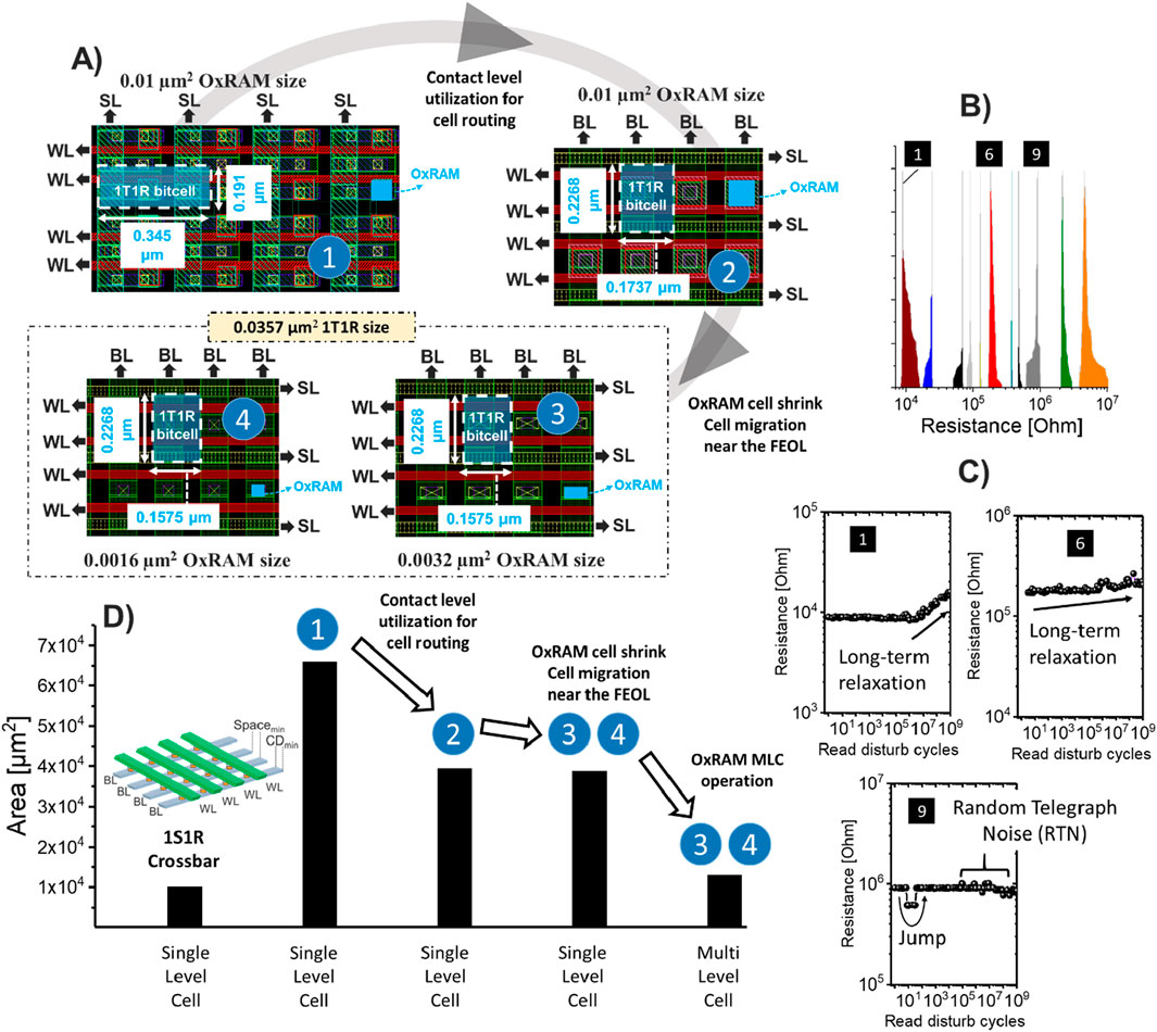
Figure 12. (A) Summary of the OxRAM-based 1T1R cell optimization approach, coupling the memory cell shrink with its migration close to the FEOL. (B) OxRAM MLC experimental probabilistic programmed resistance density at the cell level. Provided data is extracted from reading disturbance characteristics up to 109 cycles. (C) OxRAM resistance evolution with successive reading pulses, illustrating the presence of resistance fluctuations in the devices. (D) Memory area evolution for the various 1T1R cell architectural scenarios studied in this work. The provided area for MLC operated cells is based on experimental read disturb distributions presented in (B).
5 Conclusion
The ability of OxRAM-based 1T1R memory arrays to give rise to very dense architectures competitive with Crossbar architectures is elucidated. By crossing experimental data with cell design deep analysis, both OxRAM-based 1S1R-based Crossbar architectures and OxRAM-based 1T1R single memristor structures pertinence for inference computing implementation on-chip is compared. While 1S1R-based Crossbar memory structures promise 4F2 very dense memory capabilities, intrinsic limitations for their utilization as memristive element for MAC operation deployment on-chip are identified. By means of both cell architecture revolution and active material adaptation, a promising 1T1R cell is experimentally validated in 28 nm CMOS FDSOI technology. The OxRAM is integrated in the drain contact of FDSOI transistor, allowing state-of-art 0.0357 μm2 bitcell area potential. The OxRAM active material composition is optimized, resulting in 106 endurance and 11-level MLC encoding resilient to 109 inference cycles capabilities. Overall, the proposed 1T1R cell benefits from natural in-memory MAC hardware implementation relying on Ohm’s and Kirchoff’s current law coupled with very low bitcell footprint. Particularly, the proposed OxRAM-based 1T1R cell with 3-bit encoding capabilities is ∼5.1x denser than the standard BEOL OxRAM-based 1T1R cell routed integrally using BEOL metal levels, reaching only ∼1.3x bigger cell footprint than SLC 1S1R-based Crossbar technology in 28 nm node. Globally, this ensures its pertinence as memristive technological platform for in or near-memory analog Neural Network deployment.
Data availability statement
The raw data supporting the conclusions of this article will be made available by the corresponding author, upon request and without undue reservation.
Author contributions
JM: Conceptualization, Investigation, Writing–original draft, Writing–review and editing, Data curation, Formal Analysis, Validation. SB: Conceptualization, Investigation, Writing–review and editing, Project administration, Validation. DC: Investigation, Validation, Writing–review and editing, Data curation, Formal Analysis. AJ: Investigation, Validation, Writing–review and editing. AdG: Data curation, Formal Analysis, Investigation, Validation, Writing–review and editing. AS: Investigation, Validation, Writing–review and editing. J-MP: Investigation, Validation, Writing–review and editing. CoC: Investigation, Validation, Writing–review and editing. AhG: Investigation, Validation, Writing–review and editing. FB: Investigation, Validation, Writing–review and editing. ClC: Investigation, Validation, Writing–review and editing. AL: Investigation, Validation, Writing–review and editing. FA: Conceptualization, Funding acquisition, Investigation, Project administration, Resources, Validation, Writing–review and editing.
Funding
The author(s) declare that financial support was received for the research and/or publication of this article. OxRAM-based 1T1R fabrication cost has been financed through the European Research Council MYCUBE project (grant N° 820048) and French Public Autorities related NANO2022 program. This project also received funding within the HORIZON KDT- Joint Undertaking project EdgeAI in collaboration with European Union’s Research and Innovation program, under grant agreement numbers 101097300. It also benefits from the France 2030 government grant managed by the French National Research Agency (ANR-23-PEIA-0002).
Conflict of interest
The authors declare that the research was conducted in the absence of any commercial or financial relationships that could be construed as a potential conflict of interest.
Generative AI statement
The author(s) declare that no Generative AI was used in the creation of this manuscript.
Publisher’s note
All claims expressed in this article are solely those of the authors and do not necessarily represent those of their affiliated organizations, or those of the publisher, the editors and the reviewers. Any product that may be evaluated in this article, or claim that may be made by its manufacturer, is not guaranteed or endorsed by the publisher.
References
Aguirre, F., Sebastian, A., Le Gallo, M., Song, W., Wang, T., Joshua Yang, J., et al. (2024). Hardware implementation of memristor-based artificial neural networks. Nat. Commun. 15, 1974. doi:10.1038/s41467-024-45670-9
Berthelon, R., Andrieu, F., Josse, E., Bingert, R., Weber, O., Serret, E., et al. (2016). “Design/technology co-optimization of strain-induced layout effects in 14nm UTBB-FDSOI CMOS: enablement and assessment of continuous-RX designs,” in 2016 IEEE symposium on VLSI technology (Honolulu, HI, USA), 1–2. doi:10.1109/VLSIT.2016.7573425
Bourgeois, G., Meli, V., Antonelli, R., Socquet-Clerc, C., Magis, T., Laulagnet, F., et al. (2023). “Crossbar arrays based on “wall” phase-change memory (PCM) and ovonic- threshold switching (OTS) selector: a device integration challenge towards new computing paradigms in embedded applications,” in 2023 7th IEEE electron devices technology and manufacturing conference (EDTM) (Seoul, Republic of Korea), 1–3. doi:10.1109/EDTM55494.2023.10102961
Chang, M.-F., Wu, J.-J., Chien, T.-F., Liu, Y.-C., Yang, T.-C., Shen, W.-C., et al. (2014). “19.4 embedded 1Mb ReRAM in 28nm CMOS with 0.27-to-1V read using swing-sample-and-couple sense amplifier and self-boost-write-termination scheme,” in 2014 IEEE international solid-state circuits conference digest of technical papers (ISSCC) (San Francisco, CA, USA), 332–333. doi:10.1109/ISSCC.2014.6757457
Chen, Y. Y., Pourtois, G., Adelmann, C., Goux, L., Govoreanu, B., Degraeve, R., et al. (2012). Insights into Ni-filament formation in unipolar-switching Ni/HfO2/TiN resistive random access memory device. Appl. Phys. Lett. 100, 113513. doi:10.1063/1.3695078
Chou, C.-C., Lin, Z.-J., Lai, C.-A., Su, C.-I., Tseng, P.-L., Chen, W.-C., et al. (2020). “A 22nm 96KX144 RRAM macro with a aelf-tracking reference and a low ripple charge pump to achieve a configurable read window and a wide operating voltage range,” in 2020 IEEE symposium on VLSI circuits (Honolulu, HI, USA), 1–2. doi:10.1109/VLSICircuits18222.2020.9163014
Collinge, J.-P. (2014). “Multigate transistors: pushing Moore's law to the limit,” in 2014 international conference on simulation of semiconductor processes and devices (SISPAD) (Yokohama, Japan), 313–316. doi:10.1109/SISPAD.2014.6931626
Dubreuil, T., Barraud, S., Pedini, J.-M., Hartmann, J.-M., Boulard, F., Sarrazin, A., et al. (2023a). “Integration of HfO2-based 3D OxRAM with GAA stacked-nanosheet transistor for high-density embedded memory,” in ESSDERC 2023 - IEEE 53rd European solid-state device research conference (ESSDERC) (Lisbon, Portugal), 117–120. doi:10.1109/ESSDERC59256.2023.10268513
Dubreuil, T., Barraud, S., Previtali, B., Martinie, S., Lacord, J., Martin, S., et al. (2023b). “Fabrication of low-power RRAM for stateful hyperdimensional computing,” in 2023 international VLSI symposium on technology, systems and applications (VLSI-TSA/VLSI-DAT) (HsinChu, Taiwan), 1–2. doi:10.1109/VLSI-TSA/VLSI-DAT57221.2023.10134182
Golonzka, O., Arslan, U., Bai, P., Bohr, M., Baykan, O., Chang, Y., et al. (2019). “Non-volatile RRAM embedded into 22FFL FinFET technology,” in 2019 symposium on VLSI technology (Kyoto, Japan), T230–T231. doi:10.23919/VLSIT.2019.8776570
Govoreanu, B., Kar, G. S., Chen, Y.-Y., Paraschiv, V., Kubicek, S., Fantini, A., et al. (2011). “10×10nm2hf/hfox crossbar resistive ram with excellent performance, reliability and low-energy operation,” in 2011 international electron devices meeting (Washington, DC, United States), 31.6.1–31.6.4. doi:10.1109/IEDM.2011.6131652
Grenouillet, L., Castellani, N., Persico, A., Meli, V., Martin, S., Billoint, O., et al. (2021). “16kbit 1T1R OxRAM arrays embedded in 28nm FDSOI technology demonstrating low BER, high endurance, and compatibility with core logic transistors,” in 2021 IEEE international memory workshop (IMW) (Dresden, Germany), 1–4. doi:10.1109/IMW51353.2021.9439607
Hayakawa, Y., Himeno, A., Yasuhara, R., Boullart, W., Vecchio, E., Vandeweyer, T., et al. (2015). “Highly reliable TaOx ReRAM with centralized filament for 28-nm embedded application,” in 2015 symposium on VLSI circuits (VLSI circuits) (Kyoto, Japan), T14–T15. doi:10.1109/VLSIC.2015.7231381
Huang, Y.-C., Liu, S.-H., Chen, H.-S., Feng, H.-C., Li, C.-F., Yang, C.-Y., et al. (2024). “15.7 A 32Mb RRAM in a 12nm FinFet technology with a 0.0249μm2 bit-cell, a 3.2GB/S read throughput, a 10KCycle write endurance and a 10-year retention at 105°C,” in 2024 IEEE international solid-state circuits conference (ISSCC) (San Francisco, CA, United States), 288–290. doi:10.1109/ISSCC49657.2024.10454367
Ito, S., Hayakawa, Y., Wei, Z., Muraoka, S., Kawashima, K., Kotani, H., et al. (2018). “ReRAM technologies for embedded memory and further applications,” in 2018 IEEE international memory workshop (IMW) (Kyoto, Japan), 1–4. doi:10.1109/IMW.2018.8388846
Jain, P., Arslan, U., Sekhar, M., Lin, B. C., Wei, L., Sahu, T., et al. (2019). “2 embedded non-volatile ReRAM macro in 22nm FinFET technology with adative forming/set/reset schemes yielding down to 0.5V with sensing time of 5ns at 0.7V,” in 2019 IEEE international solid-state circuits conference - (ISSCC) (San Francisco, CA, United States), 212–214. doi:10.1109/ISSCC.2019.8662393
Kau, D., Tang, S., Karpov, I.-V., Dodge, R., Klehn, B., Kalb, J., et al. (2009). “A stackable cross point phase change memory,” in 2009 IEEE international electron devices meeting (IEDM) (Baltimore, MD, United States), 1–4. doi:10.1109/IEDM.2009.5424263
Lepri, N., Gibertini, P., Mannocci, P., Pirovano, A., Tortorelli, I., Fantini, P., et al. (2023). “In-memory neural network accelerator based on phase change memory (PCM) with one-selector/one-resistor (1S1R) structure operated in the subthreshold regime,” in 2023 IEEE international memory workshop (IMW) (Monterey, CA, United States), 1–4. doi:10.1109/IMW56887.2023.10145949
Li, H., Li, K.-S., Lin, C.-H., Hsu, J.-L., Chiu, W.-C., Chen, M.-C., et al. (2016). “Four-layer 3D vertical RRAM integrated with FinFET as a versatile computing unit for brain-inspired cognitive information processing,” in 2016 IEEE symposium on VLSI technology (Honolulu, HI, USA), 1–2. doi:10.1109/VLSIT.2016.7573431
Minguet Lopez, J., Barraud, S., Dampfhoffer, M., Souhaité, A., Dubreuil, T., Pedini, J.-M., et al. (2025). “Compact MEOL OxRAM with 14 conductance levels for dense embedded inference computing,” in Accepted in 2025 IEEE international reliability physics symposium (IRPS). Monterey, CA, United States.
Minguet Lopez, J., Dampfhoffer, M., Navarro, G., Bernard, M., Carabasse, C., Castellani, N., et al. (2024). “1S1R multi-level-cell for dense quantized recurrent spiking neural network inference computing,” in 2024 international conference on solid state devices and materials (Himeji, Japan). doi:10.7567/SSDM.2024.B-2-02
Minguet Lopez, J., Hudeley, L., Grenouillet, L., Alfaro Robayo, D., Sandrini, J., Navarro, G., et al. (2021). “Elucidating 1S1R operation to reduce the read voltage margin variability by stack and programming conditions optimization,” in 2021 IEEE international reliability physics symposium (IRPS) (Monterey, CA, United States), 1–6. doi:10.1109/IRPS46558.2021.9405195
Molas, G., and Nowak, E. (2021). Advances in emerging memory technologies: from data storage to artificial intelligence. Appl. Sci. 11, 11254. doi:10.3390/app112311254
Moroz, V. (2011). Transition from planar MOSFETs to FinFETs and its impact on design and variability. Berkeley Microlab. Available at: https://microlab.berkeley.edu/text/seminars/slides/moroz.pdf
Moroz, V. (2016). “Technology inflection points: planar to FinFET to nanowire,” in International symposium on physical design (ISPD) (Santa Rosa, CA, United States).
Murmann, B. (2021). Mixed-signal computing for deep neural network inference. IEEE Trans. Very Large Scale Integration (VLSI) Syst. 29 (1), 3–13. doi:10.1109/TVLSI.2020.3020286
Nagel, M., Fournarakis, M., Ali, A. R., Bondarenko, Y., Van Baalen, M., and Blankevoort, T. (2021). A white paper on neural network quantization. arXiv. preprint arXiv:2106.08295. doi:10.48550/arXiv.2106.08295
Planes, N., Weber, O., Barral, V., Haendler, S., Noblet, D., Croain, D., et al. (2012). “28nm FDSOI technology platform for high-speed low-voltage digital applications,” in 2012 symposium on VLSI technology (VLSIT) (Honolulu, HI, USA), 133–134. doi:10.1109/VLSIT.2012.6242497
Raghavan, N., Pey, K. L., Liu, W., Wu, X., Li, X., and Bosman, M. (2011). Evidence for compliance controlled oxygen vacancy and metal filament based resistive switching mechanisms in RRAM. Microelectron. Eng. 88 (7), 1124–1128. doi:10.1016/j.mee.2011.03.027
Reganaz, L., Deleruyelle, D., Rafhay, Q., Minguet Lopez, J., Castellani, N., Nodin, J.-F., et al. (2023). “Investigation of resistance fluctuations in ReRAM: physical origin, temporal dependence and impact on memory reliability,” in 2023 IEEE international reliability physics symposium (IRPS) (Monterey, CA, United States), 1–6. doi:10.1109/IRPS48203.2023.10117882
Sandrini, J., Grenouillet, L., Meli, V., Castellani, N., Hammad, I., Bernasconi, S., et al. (2019). “OxRAM for embedded solutions on advanced node: scaling perspectives considering statistical reliability and design constraints,” in 2019 IEEE international electron devices meeting (IEDM) (San Francisco, CA, United States), 30.5.1–30.5.4. doi:10.1109/IEDM19573.2019.8993484
Shen, W. C., Mei, C. Y., Chih, Y.-D., Sheu, S.-S., Tsai, M.-J., King, Y.-C., et al. (2012). “High-K metal gate contact RRAM (CRRAM) in pure 28nm CMOS logic process,” in 2012 international electron devices meeting (San Francisco, CA, United States), 31.6.1–31.6.4. doi:10.1109/IEDM.2012.6479146
Shulaker, M. M., Wu, T. F., Pal, A., Zhao, L., Nishi, Y., Saraswat, K., et al. (2014). “Monolithic 3D integration of logic and memory: carbon nanotube FETs, resistive RAM, and silicon FETs,” in 2014 IEEE international electron devices meeting (San Francisco, CA, United States), 27.4.1–27.4.4. doi:10.1109/IEDM.2014.7047120
Sze, V. (2019). “Efficient processing of deep neural networks: from algorithms to hardware architectures,” in NEURIPS (Vancouver, Canada).
Wan, W., Kubendran, R., Schaefer, C., Burc, E. S., Zhang, W., Wu, D., et al. (2022). A compute-in-memory chip based on resistive random-access memory. Nature 608, 504–512. doi:10.1038/s41586-022-04992-8
Wang, C., Wu, H., Gao, B., Dai, L., Deng, N., Sekar, D. C., et al. (2016). Relaxation effect in RRAM arrays: demonstration and characteristics. IEEE Electron Device Lett. 37 (2), 182–185. doi:10.1109/LED.2015.2508034
Wu, J., Mo, F., Saraya, T., Hiramoto, T., and Kobayashi, M. (2020). “A monolithic 3D integration of RRAM array with oxide semiconductor FET for in-memory computing in quantized neural network AI applications,” in 2020 IEEE symposium on VLSI technology (Honolulu, HI, USA), 1–2. doi:10.1109/VLSITechnology18217.2020.9265062
Wu, X., Mei, S., Bosman, M., Raghavan, N., Zhang, X., Cha, D., et al. (2015). Evolution of filament formation in Ni/HfO2/SiOx/Si-based RRAM devices. Adv. Electron. Mater. 1, 1500130. doi:10.1002/aelm.201500130
Xie, M., Jia, Y., Nie, C., Liu, Z., Tang, A., Fan, S., et al. (2023). Monolithic 3D integration of 2D transistors and vertical RRAMs in 1T–4R structure for high-density memory. Nat. Commun. 14, 5952. doi:10.1038/s41467-023-41736-2
Xue, C.-X., Chen, W.-H., Liu, J. S., Li, J.-F., Lin, W.-Y., Lin, W.-E., et al. (2019). “24.1 A 1Mb multibit ReRAM computing-in-memory macro with 14.6ns parallel MAC computing time for CNN based AI edge processors,” in 2019 IEEE international solid-state circuits conference - (ISSCC) (San Francisco, CA, United States), 388–390. doi:10.1109/ISSCC.2019.8662395
Keywords: OxRAM, memristor, 1T1R, in-memory computing, 1S1R, Crossbar
Citation: Minguet Lopez J, Barraud S, Cooper D, Jannaud A, Grenier A, Souhaité A, Pedini J-M, Comboroure C, Gharbi A, Boulard F, Castan C, Lambert A and Andrieu F (2025) Rethinking 1T1R architecture and OxRAM stack for memristive neural network inference in-memory. Front. Nanotechnol. 7:1549547. doi: 10.3389/fnano.2025.1549547
Received: 21 December 2024; Accepted: 28 February 2025;
Published: 26 March 2025.
Edited by:
Ying-Chen Chen, Arizona State University, United StatesReviewed by:
Xiaoxin Xu, Chinese Academy of Sciences (CAS), ChinaRuomeng Huang, University of Southampton, United Kingdom
Copyright © 2025 Minguet Lopez, Barraud, Cooper, Jannaud, Grenier, Souhaité, Pedini, Comboroure, Gharbi, Boulard, Castan, Lambert and Andrieu. This is an open-access article distributed under the terms of the Creative Commons Attribution License (CC BY). The use, distribution or reproduction in other forums is permitted, provided the original author(s) and the copyright owner(s) are credited and that the original publication in this journal is cited, in accordance with accepted academic practice. No use, distribution or reproduction is permitted which does not comply with these terms.
*Correspondence: Joel Minguet Lopez, joel.minguetlopez@cea.fr