 Ruobing Bai
- 1Department of Chemistry, University of Pittsburgh, Pittsburgh, PA, United States
- 2Department of Electrical and Computer Engineering, University of Pittsburgh, Pittsburgh, PA, United States
- 3Department of Biological Sciences, University of Pittsburgh, Pittsburgh, PA, United States
This paper reports the fabrication of silicon PN diode by using DNA nanostructure as the etching template for SiO2 and also as the n-dopant of Si. DNA nanotubes were deposited onto p-type silicon wafer that has a thermal SiO2 layer. The DNA nanotubes catalyze the etching of SiO2 by HF vapor to expose the underlying Si. The phosphate groups in the DNA nanotube were used as the doping source to locally n-dope the Si wafer to form vertical P-N junctions. Prototype PN diodes were fabricated and exhibited expected blockage behavior with a knee voltage of ca. 0.7 V. Our work highlights the potential of DNA nanotechnology in future fabrication of nanoelectronics.
Introduction
As the demand for high performance of electronic devices in terms of power, speed and density continues to grow, there is an increasing need for new technologies to produce nanoelectronic devices (Ito and Okazaki, 2000; Thompson and Parthasarathy, 2006). A major driving force of the semiconductor industry has been the continuous reduction of the feature size and the overall manufacturing cost (Peercy, 2000; Charles, 2005). As a result, there has been persistent interests in developing technologies for high-resolution, low-cost, and large-scale fabrication of semiconductor materials.
Photolithography is the dominate patterning method for high-volume fabrication of electronic devices (Seisyan, 2011). Although this method is very successful and widely used in industry and research, photolithography requires a clean environment, expensive masks and equipment, all of which increase the overall manufacturing costs, especially at small scale (Wu et al., 2002). In addition, Si-based nanoelectronics typically require multiple doping types and doping concentrations in different regions of the wafer. Each doping step requires a separate cycle of lithography to define the doped region, which further increases the manufacturing cost and complexity (Costner et al., 2009; Škereň et al., 2018).
In recent years, DNA-based nanofabrication has drawn increasing attention due to its potential in realizing high-resolution low-cost patterning. We and others have reported various approaches to achieve high-resolution pattern transfer from DNA nanostructure templates to many substrates, such as SiO2, Si, polymers, graphite, and self-assembled monolayers (Surwade et al., 2011; Surwade et al., 2013; Zhou et al., 2015; Surwade et al., 2016; Ricardo et al., 2017; Tian et al., 2017). A major motivation of these studies is for the future application and integration of DNA nanotechnology in the nanoelectronics industry. In this context, DNA-based nanofabrication has unique advantages when compared to the traditional, photolithography-based approaches. First, DNA-based nanofabrication combines the best features of top-down and bottom-up fabrication methods, in the sense that it is based on self-assembly (a unique feature of bottom-up methods) but can also produce almost any arbitrary patterns (used to be a unique feature of top down methods) (Biswas et al., 2012; Arole and Munde, 2014). Second, the cost of the DNA template for 2D patterning is extremely low (on the order of ca. $1/m2), which may enable low-cost, high-resolution patterning in very large scales. (Zhang et al., 2013).
DNA nanostructures are not only useful as templates for nanofabrication, they can also be used as dopant. Inspired by monolayer doping (Ho et al., 2009; Gao et al., 2018), we recently reported the use of DNA nanostructures to achieve site-specific doping of Si. In this approach, a DNA nanostructure was deposited onto a Si wafer and the phosphorous atoms (an n-type dopant) naturally present in the DNA were thermally diffused into the Si wafer to form n-doped regions. Unlike the traditional doping process, where the doped regions are defined by photolithography, the doped regions in this approach are defined by the shape of the DNA nanostructure. By using self-assembled monolayer as an intermediate, we also demonstrated p-doping of Si. This approach makes it possible to tune the doping level by adjusting the density of DNA molecules (e.g., one layer vs. two layers) or even introducing new types of dopants via chemically functionalization. Therefore, this DNA-based doping strategy has great potential to reduce the overall complexity of the fabrication of Si nanoelectronics. (Bai et al., 2020).
With various forms of DNA-enabled patterning and doping methods at hand, it is now possible to integrate DNA nanotechnology into the fabrication of nanoelectronics devices, potentially reducing or even eliminating photolithography and the associated etching, deposition, and doping steps. Such a goal, if realized, could lead to a drastic reduction of the manufacturing cost of nanoelectronic devices. In our previous work, we demonstrated the fabrication of prototype filed effect devices from a native Si substrate that has been site-specifically doped by DNA nanostructure templates. In this work, we describe the fabrication of vertical PN diodes by using DNA nanostructures to pattern and dope a p-type Si substrate.
Methods
Materials
p-type silicon wafers [100] with native oxide layers (Boron doped, 1–10 Ω·cm, double side polished) were purchased from University Wafer. DNA strands for the synthesis were purchased from IDT. Sulfuric acid, 2-Amino-2-(hydroxymethyl)-1,3-propanediol (Trizma base or Tris, ≥99.9%), ethylenediaminetetraacetic acid (EDTA, ≥99%), acetic acid (≥99.7%), magnesium acetate tetrahydrate (≥99%), hydrogen peroxide solution (30% wt. % in water), sodium chloride, methanol and ethanol were purchased from Sigma-Aldrich (St. Louis, MO). Nanopure water (18.3 MΩ) was obtained using a water purification system (Barnstead MicroPure Standard, Thermo Scientific, Waltham, MA) and used throughout the entire experiment to prepare chemical solutions and clean experimental samples.
Atomic force microscopy (AFM) and scanning electron microscopy (SEM) characterization
Throughout the study, AFM topography images were acquired in tapping mode in air using an Asylum MFP-3D Atomic Force Microscope with HQ:NSC15/Al BS AFM probes (325 kHz, 40 N/m) purchased from MikroMasch (NanoAndMore United States). SEM images were obtained by a ZEISS Sigma 500 VP microscope.
Synthesis and deposition of DNA nanotubes onto silicon wafer
The synthesis of DNA nanotubes here were based on previously published procedures. (Liu et al., 2006; Tian et al., 2017). The nanotube was prepared by self-polymerization of a single stranded DNA of the following sequence: 5′- CCAAGCTTGGACTTCAGGCCTGAAGTGGTCATTCGAATGACCTGAGCGCTCA-3′. We diluted the DNA strand in 10 × TAE-Mg2+ buffer (400 mM tris-acetic acid, 10 mM EDTA, 125 mM Mg2+, pH = 8.0) to a final concentration of 2 μM. The DNA single strand solution was then slowly cooled down from 95°C to 23°C in 2 days and stored at 4°C overnight for the subsequent deposition step.
The p-type Si substrate was cleaned by piranha solution [3/7 (v/v) hydrogen peroxide/sulfuric acid solution] for 30 min (Warning: piranha solution reacts violently with organic compounds, please handle in a fume hood and use proper personal protection equipment). The clean substrate was placed in a furnace at 900°C for 3 h to grow SiO2, and the surface of the substrate was cleaned again by piranha solution. The prepared DNA sample (10 µL) was then pipetted onto the cleaned wafer and placed in a plastic petri dish. We then inserted a wet Kimwipe between the lid and the bottom to maintain high humidity inside the petri dish and reduce the evaporation. After 40 min of undisturbed incubation, we dried the Si substrate with a stream of N2 gas, then immersed it into an 8/2 (v/v) ethanol/water solution for 20 s to remove salt residues on the surface and then dried the substrate with N2 gas again. This washing and drying process was repeated 3 times.
Selective etching of SiO2 under the DNA nanostructure template
The selective etching of SiO2 is based on the DNA-enhanced HF-etching of SiO2, reported in our previous work. (Zhou et al., 2015). Briefly, we exposed the Si/SiO2 substrate with deposited DNA nanotubes to HF vapor. The etching of SiO2 is much faster in the presence of DNA nanostructure than in its absence. We control the etching time to remove all SiO2 under the DNA nanotubes to produce trenches while leaving a thin SiO2 layer everywhere else. The thickness of the remaining SiO2 was measured by ellipsometry, and the depth of the etched trench was measured by AFM. From these two measurements, we can determine if the SiO2 under the DNA nanotube was completely removed.
Site-specific doping of Si by DNA
The procedure was adopted from our previous work (Bai et al., 2020). Briefly, after DNA-mediated etching, the Si substrate was subjected to a UV/O3 treatment (Novascan UV/ozone cleaner) for 3 h to oxidize the DNA nanotube. Our previous work showed that the oxidation leaves a residue, presumably phosphates. Then the sample was coated by a 20 nm of Al2O3 grown by atomic layer deposition (ALD) using a Cambridge Nanotech Fiji ALD instrument. The role of the Al2O3 layer is to minimize the loss and the lateral diffusion of the phosphate dopants. After depositing the Al2O3 capping layer, the samples were subjected to a rapid thermal annealing (RTA) process using a Surface Science Integration RTA Solaris 75 instrument. During this process, the temperature of the wafer rose to 1,000°C within 20 s and kept at this temperature for 10 s. Then the temperature was cooled down to 150°C within 3 min. After the RTA treatment, we used H3PO4 solution (2 M) to remove the Al2O3 capping layer and used a hot piranha solution to wash away (60 min) any residues on the surface. Finally, the sample was washed with deionized water and dried with N2 gas.
Device fabrication and electrical measurements
The dielectric layer and metal contacts were patterned by electron beam lithography using a Raith e-Line system. In order to reduce leakage current, we deposited a 20 nm of HfO2 layer by ALD (Cambridge Nanotech Fiji ALD) to cover all the surface where the metal contact would be later deposited except for the small area near the DNA-doped region. The metal contacts consist of 2 nm of Ti and 60 nm of Au evaporated using a Plassys electron beam evaporator. Finally, the metal contacts were wire-bonded to a chip carrier using aluminum wires. Electrical characteristics were measured using a Keithley 4200A-SCS Parameter Analyzer in air at room temperature.
Results and discussion
Fabrication of P-N junction using DNA-based doping
We used DNA nanotubes to form n-type site-specific doped regions on a p-type silicon wafer, thereby forming a vertical PN junction. The method for forming n-type site-specific doping here follows our previous work where we use the phosphates in DNA as the doping source. First, we prepared DNA nanotubes by self-assembly of one short single-strand DNA containing four palindromic segments, which allows the strands to self-polymerize into nanotubes. We then deposited the DNA nanotubes onto a p-type wafer that has a 40 nm thick of SiO2 (Figure 1A). (Bai et al., 2021) Once deposited, these DNA nanotubes have a width of ca. 70 nm and a height of ca. 2.0 nm. The small thickness is consistent with the expected drying-induced collapse of the tube structure after deposition onto the Si substrate.
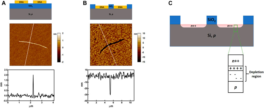
FIGURE 1. Schematic diagrams, AFM images and cross sections (the vertical lines in the AFM images indicate the locations of the cross section) of the silicon wafer during the patterning and doping process. (A), DNA nanotubes deposited onto a Si/SiO2 substrate. (B), Trench formed as a result of the selective removal of the SiO2 underneath the DNA through DNA-enhanced etching of SiO2. (C), Schematic diagram of the sample after the DNA-based doping. Multiple doped regions were shown but devices were fabricated on an individual doped region.
To dope Si, we first exposed the wafer to HF vapor to remove all the SiO2 under the DNA nanotubes, while leaving about 30 nm of SiO2 everywhere else to eliminate undesirable doping of the background region during the RTA (Figure 1B). The SiO2 underneath the DNA nanotube was etched faster because DNA absorbs water, which is a catalyst for HF etching of SiO2. After the etching, the DNA nanotubes left narrow trenches on the wafer. We used ellipsometry and AFM to measure the average thickness of the SiO2 on the wafer and the depth of the trench formed by the DNA nanotube, respectively. The two measurement gave very similar values, ca. 30 nm, indicating that the SiO2 under the DNA nanotubes has been completely removed to expose the underlying Si.
The sample was then treated with UV/O3 to remove the organic components of the DNA. During this process, carbon and nitrogen atoms within the DNA and the buffer residue, if any, are removed by O3 oxidation, leaving a phosphate residue that will serve as the doping source. While not investigated in this study, it will be important to maintain an ultraclean environment to minimize undesired deactivation of dopants due to contamination from the DNA solution and ambient. The wafer was then covered with 20 nm of Al2O3 to limit the lateral diffusion and desorption of the dopants. To initiate the doping, the wafer was treated with RTA for 10 s at 1,000°C. After cooling to r.t., it was washed with H3PO4 to remove the Al2O3 capping layer and washed with piranha solution to remove any inorganic residue on the surface. We previously showed that this process resulted in high level n-doping of native Si wafer, achieving dopant concentration of 6.4 × 1018 cm−3. The p-type wafer used in this study was doped by boron and has a resistivity of 1–10 Ω·cm, from which we estimated a p-dopant concentration of ca. 1016 cm−3. Therefore, after the heavy n-doping by DNA nanotube, nanowire-shaped vertical P-N junctions will be formed on the Si wafer (Figure 1C).
Fabrication of PN diodes
We used electron beam lithography to pattern electrodes on a single nanowire-shaped PN junction region (Figures 2A, B) to form a vertical PN diode. Before patterning metal electrodes, we deposited a thin layer of HfO2 (20 nm) to cover the whole wafer except the targeted area containing the nanowire-shaped PN junction. After patterning electrodes, we used wire bonding to connect the electrodes to a chip carrier to avoid mechanical damage of the HfO2 layer during electrical measurement. Figure 2C is a photograph of the device after wire bonding. A schematic diagram of the sample ready for testing is also shown in Figure 2D, where two identical devices were shown. Control devices were also fabricated on the same wafer in areas without DNA nanotubes; in the absence of DNA nanotubes, the SiO2 layer was not completely etched away to expose Si and therefore such region was not doped by DNA and also covered by the HfO2. Current measured from the control device are due to leakage through the HfO2 layer.
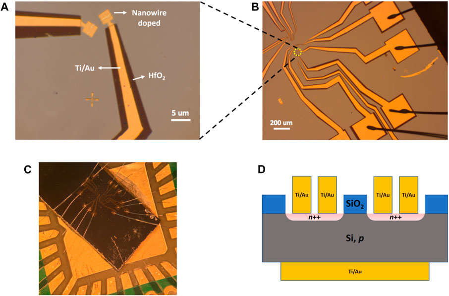
FIGURE 2. Fabrication of PN diodes from a single “nanowire”-shaped doped region. (A,B), Optical image of the patterned electrodes. (C), Photograph of the device after wire bonding. (D), Schematic diagram of the PN diode.
Characterization of PN diode
To evaluate the electrical characteristics of the PN diode, we wired the device according to Figure 3A. The current-voltage (I-V) characteristic of the device is shown in Figures 3B, C. It can be seen that the device fabricated from the DNA-doped region exhibits the characteristic blockage behavior of the PN diode, while the control device fabricated on non-doped region does not. The small current measured from the control device also confirms that the leakage current through the HfO2 coating is negligible. Further analysis shows that the knee voltage of the PN diode is ca. 0.7 V, which is consistent with the theoretical value of Si (Sawant and Baliga, 2000; Ghazi et al., 2009). The result confirms the successful site-specific SiO2 etching, n-doping by DNA, formation of PN junction, and fabrication of vertical PN diodes. However, the I-V curve also gives an ideality factor (ca. 6.5, within 0.2–0.5 V of forward bias) that is significantly larger than 1, suggesting that the device characteristics are far from that of ideal silicon behavior and possibility involve trap-assisted tunneling, carrier leakage, and large serial resistance. (Martil and Diaz, 1991; Zhu et al., 2009).
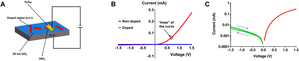
FIGURE 3. Characterization of the PN diode. (A), Schematic diagram for the test of the device. (B), I-V curves for the “nanowire” doped region and non-doped region. (C), semilog plot of I-V curve. Arrows indicate I-V scan direction.
Conclusion
In summary, we have successfully formed vertical PN junctions by using DNA nanotube to dope a p-type Si substrate. PN diodes were fabricated from these junctions and their electrical characteristics are consistent with those of their conventional counterparts. The successful fabrication of PN diodes highlights the potential of using DNA nanostructure to pattern and dope Si and based on which, to manufacture functional nanoelectronic devices. That being said, we recognize that there are still many challenges that need to be addressed before this technology can make a real impact on semiconductor manufacturing. In this regard, we are investigating ways to combine conventional lithography with DNA nanotechnology for large scale fabrication of devices. For example, use existing lithography techniques to define a micrometer-sized area, within which self-assembled DNA nanostructures, such as DNA 2D lattice, defines multiple doping areas and devices. We hope that this work will catalyze further research on DNA-based nanofabrication and ultimately a simpler, lower-cost manufacturing approach based on biomolecular templates.
Data availability statement
The raw data supporting the conclusion of this article will be made available by the authors, without undue reservation.
Author contributions
RB: Data curation, Investigation, Writing–original draft, Writing–review and editing. YL: Data curation, Investigation, Writing–review and editing. BZ: Data curation, Investigation, Writing–review and editing. BC: Data curation, Investigation, Writing–review and editing. FX: Conceptualization, Funding acquisition, Writing–review and editing. HL: Conceptualization, Funding acquisition, Project administration, Resources, Supervision, Writing–review and editing.
Funding
The author(s) declare financial support was received for the research, authorship, and/or publication of this article. HL and FX acknowledge partial support from NSF CMMI-2229131 and ECCS-2235294; YL and FX acknowledge support from NSF ECCS-1943683.
Conflict of interest
The authors declare that the research was conducted in the absence of any commercial or financial relationships that could be construed as a potential conflict of interest.
The author(s) declared that they were an editorial board member of Frontiers, at the time of submission. This had no impact on the peer review process and the final decision.
Publisher’s note
All claims expressed in this article are solely those of the authors and do not necessarily represent those of their affiliated organizations, or those of the publisher, the editors and the reviewers. Any product that may be evaluated in this article, or claim that may be made by its manufacturer, is not guaranteed or endorsed by the publisher.
References
Arole, V., and Munde, S. (2014). Fabrication of nanomaterials by top-down and bottom-up approaches-an overview. JAAST:Material Science (Special Issue), 1, 89–93.
Bai, R., Du, Y., Xu, A., Hu, Y., Erickson, J. R., Hui, L., et al. (2020). DNA-Based strategies for site-specific doping. Adv. Funct. Mater. 31, 2005940. doi:10.1002/adfm.202005940
Bai, R., Du, Y., Xu, A., Hu, Y., Erickson, J. R., Hui, L., et al. (2021). DNA-Based strategies for site-specific doping. Adv. Funct. Mater. 31 (1), 2005940. doi:10.1002/adfm.202005940
Biswas, A., Bayer, I. S., Biris, A. S., Wang, T., Dervishi, E., and Faupel, F. (2012). Advances in top–down and bottom–up surface nanofabrication: techniques, applications and future prospects. Adv. Colloid Interface Sci. 170 (1-2), 2–27. doi:10.1016/j.cis.2011.11.001
Costner, E. A., Lin, M. W., Jen, W.-L., and Willson, C. G. (2009). Nanoimprint lithography materials development for semiconductor device fabrication. Annu. Rev. Mater. Res. 39, 155–180. doi:10.1146/annurev-matsci-082908-145336
Gao, X., Guan, B., Mesli, A., Chen, K., and Dan, Y. (2018). Deep level transient spectroscopic investigation of phosphorus-doped silicon by self-assembled molecular monolayers. Nat. Commun. 9 (1), 118. doi:10.1038/s41467-017-02564-3
Ghazi, H. E., Jorio, A., and Zorkani, I. (2009). Analysis of temperature effect on IV characteristics of silicon (npn) emitter-base. Moroc. J. Condens. Matter 11 (2), 30–34.
Ho, J. C., Yerushalmi, R., Smith, G., Majhi, P., Bennett, J., Halim, J., et al. (2009). Wafer-scale, sub-5 nm junction formation by monolayer doping and conventional spike annealing. Nano Lett. 9 (2), 725–730. doi:10.1021/nl8032526
Ito, T., and Okazaki, S. (2000). Pushing the limits of lithography. Nature 406 (6799), 1027–1031. doi:10.1038/35023233
Liu, H., Chen, Y., He, Y., Ribbe, A. E., and Mao, C. (2006). Approaching the limit: can one DNA oligonucleotide assemble into large nanostructures? Angew. Chem. Int. Ed. 45 (12), 1942–1945. doi:10.1002/anie.200504022
Martil, I., and Diaz, G. G. (1991). A laboratory experiment for DC characterization of p-n devices. Eur. J. Phys. 12 (3), 149–152. doi:10.1088/0143-0807/12/3/010
Peercy, P. S. (2000). The drive to miniaturization. Nature 406 (6799), 1023–1026. doi:10.1038/35023223
Ricardo, K. B., Xu, A., Salim, M., Zhou, F., and Liu, H. (2017). Deposition of DNA nanostructures on highly oriented pyrolytic graphite. Langmuir 33 (16), 3991–3997. doi:10.1021/acs.langmuir.6b03836
Sawant, S., and Baliga, B. J. (2000). Current saturation control in silicon emitter switched thyristors. Solid-State Electron. 44 (1), 133–142. doi:10.1016/s0038-1101(99)00217-8
Seisyan, R. (2011). Nanolithography in microelectronics: a review. Tech. Phys. 56 (8), 1061–1073. doi:10.1134/s1063784211080214
Škereň, T., Pascher, N., Garnier, A., Reynaud, P., Rolland, E., Thuaire, A., et al. (2018). CMOS platform for atomic-scale device fabrication. Nanotechnology 29 (43), 435302. doi:10.1088/1361-6528/aad7ab
Surwade, S., Zhou, F., Li, Z., Powell, A., O'Donnell, C., and Liu, H. (2016). Nanoscale patterning of self-assembled monolayers using DNA nanostructure templates. Chem. Commun. 52 (8), 1677–1680. doi:10.1039/c5cc08183a
Surwade, S. P., Zhao, S., and Liu, H. (2011). Molecular lithography through DNA-mediated etching and masking of SiO2. J. Am. Chem. Soc. 133 (31), 11868–11871. doi:10.1021/ja2038886
Surwade, S. P., Zhou, F., Wei, B., Sun, W., Powell, A., O’Donnell, C., et al. (2013). Nanoscale growth and patterning of inorganic oxides using DNA nanostructure templates. J. Am. Chem. Soc. 135 (18), 6778–6781. doi:10.1021/ja401785h
Thompson, S. E., and Parthasarathy, S. (2006). Moore's law: the future of Si microelectronics. Mater. Today 9 (6), 20–25. doi:10.1016/s1369-7021(06)71539-5
Tian, C., Kim, H., Sun, W., Kim, Y., Yin, P., and Liu, H. (2017). DNA nanostructures-mediated molecular imprinting lithography. ACS Nano 11 (1), 227–238. doi:10.1021/acsnano.6b04777
Wu, M.-H., Park, C., and Whitesides, G. M. (2002). Fabrication of arrays of microlenses with controlled profiles using gray-scale microlens projection photolithography. Langmuir 18 (24), 9312–9318. doi:10.1021/la015735b
Zhang, G., Surwade, S. P., Zhou, F., and Liu, H. (2013). DNA nanostructure meets nanofabrication. Chem. Soc. Rev. 42 (7), 2488–2496. doi:10.1039/c2cs35302d
Zhou, F., Michael, B., Surwade, S. P., Ricardo, K. B., Zhao, S., and Liu, H. (2015). Mechanistic study of the nanoscale negative-tone pattern transfer from DNA nanostructures to SiO2. Chem. Mater. 27 (5), 1692–1698. doi:10.1021/cm5044914
Keywords: DNA nanotechnology, lithography, semiconductor, nanofabrication, doping
Citation: Bai R, Liu Y, Zhang B, Chen B, Xiong F and Liu H (2024) DNA-based doping and fabrication of PN diodes. Front. Nanotechnol. 6:1291328. doi: 10.3389/fnano.2024.1291328
Received: 09 September 2023; Accepted: 08 February 2024;
Published: 21 February 2024.
Edited by:
John Fourkas, University of Maryland, United StatesReviewed by:
Mohammad K. Anvarifard, University of Guilan, IranYaping Dan, Shanghai Jiao Tong University, China
Copyright © 2024 Bai, Liu, Zhang, Chen, Xiong and Liu. This is an open-access article distributed under the terms of the Creative Commons Attribution License (CC BY). The use, distribution or reproduction in other forums is permitted, provided the original author(s) and the copyright owner(s) are credited and that the original publication in this journal is cited, in accordance with accepted academic practice. No use, distribution or reproduction is permitted which does not comply with these terms.
*Correspondence: Feng Xiong, f.xiong@pitt.edu; Haitao Liu, hliu@pitt.edu
†These authors have contributed equally to this work