 Ying-Chen Chen
95% of researchers rate our articles as excellent or good
Learn more about the work of our research integrity team to safeguard the quality of each article we publish.
Find out more
BRIEF RESEARCH REPORT article
Front. Nanotechnol. , 22 November 2021
Sec. Nanomaterials
Volume 3 - 2021 | https://doi.org/10.3389/fnano.2021.772234
This article is part of the Research Topic Emerging Neuromorphic Electronics and Materials for Post-Moore Computing Era View all 6 articles
A graphite-based RRAM device with a self-rectifying characteristic named “non-linearity (NL)” is developed for a high-density crossbar array for in-memory computing with low power and high scalability. Meanwhile, the reprogrammable functions are presented in self-selected RRAM as a promising candidate for one-time programmable (OTP) in the emerging memory-embedded applications such as security, system-on-chip (SoC), and Internet of Things (IoT).
In the era of computational and information technologies renovation such as artificial intelligence (AI), Internet of Things (IoT), edge computing, and in-memory computing paradigm, the emerging memory technology with high-density storage, large bandwidth, and low power consumption has been rapidly developed over decades. With the simple crossbar structure featuring 4F2 of footprint, resistive random-access memory (RRAM) is a promising candidate for next-generation non-volatile memory technologies for both data storage and in-memory computing, owing to its ultra-low power consumption, simple structure, and high scalability (Park et al., 2013; Liu et al., 2016; Huang and Lee, 2017; Moon et al., 2018). Despite the simple structure of RRAM being beneficial for the high-density memory application, sneak-path currents (SPCs) in the crossbar array resulting in crosstalk have attracted considerable attention. The interference currents from neighboring cells caused the read error and false programming and are usually resolved by integration of a selection device, for example, transistor, diode, and selector, called “1T-1R” or “1S-1R” configurations (Sungho Kim et al., 2014; Sharma et al., 2015; Lim et al., 2016; Chen et al., 2017). However, this approach leads to high cost, fabrication complexity, energy overhead, and hindered scalability. Consequently, accessing a selected memory cell in the cross-point array with interference robustness and SPC immunity is the major challenge for high-density memory arrays (Sungho Kim et al., 2014; Lim et al., 2016; Doi et al., 2018). In other words, self-rectified memory is beneficial for future high-density storage and in-memory computing applications.
On the other hand, one-time programmable (OTP) memory enables the chip unit identification and circuit unit adaptation, and repair for cache (Chen et al., 2021). The OTP memory has become promising for embedded memory applications for its cost-effectiveness, feasibility for integration, and data retention. However, data can only be written once and cannot be revised, in which the users compromised with the risk of miss-programming. Polysilicon is utilized as the fuse element in prior CMOS technologies before utilizing the high-k metal gate in the front-end technology (Chen et al., 2017; Cheng et al., 2018; Doi et al., 2020; Chen et al., 2021). With high demands on computing configurations, the logic process-compatible non-volatile OTP utilizing the resistive memory is critical for recent applications, namely, security for data storage, security, Internet of Things, and modern system-on-chip (Kulkarni et al., 2021; Liu et al., 2018; Okuno et al., 2020; Shamsoshoara et al., 2020; Yang et al., 2020). This results in challenges, such as, increase in the fuse bit counts, overall area, large power consumption, and reliability. In this work, self-rectified graphite-based reprogrammable one-time programmable (RS-OTP) memory is presented for high-performance computing and embedded applications.
The RRAM devices with a varied feature size of 400 nm, 600 nm, 800 nm, and 1 μm have been fabricated. With starting substrates of heavily doped N + Si wafers, titanium nitride (TiN) of 200 nm was deposited as the bottom electrode (BE). Then 3, 5, 8, and 10 nm of graphite, followed by 6 nm of HfOx, were deposited as resistive switching dielectric layers for bilayer structures by radio frequency (RF) sputtering. Platinum of 165 nm was then deposited as top electrodes, followed by the lift-off process for RRAM devices. The HfOx (11 nm) single-layer, SiOx (6 nm)/graphite (5 nm), and HfOx (4 nm)/SiOx (9 nm) bilayer devices are fabricated, as in Figure 1A. The RRAM cell is filled in the SiOx isolation via, which formed by SiOx encapsulation (100 nm). Platinum is grounded while applying the voltage at TiN as the bottom electrode. The transmission electron microscopy (TEM) image of the H6G5 stacked device was analyzed in our previous work, and the graphite is examined in the crystallographic plane of (211) by X-ray diffraction (XRD) and energy dispersive X-ray spectrum (EDX) line scan results (Ki Hong et al., 2011; Chen et al., 2018a). The abbreviations for a single-layer (e.g., H11) and bilayer device structures (e.g., H6G3, H6G5, H6G8, H6G10, and H4S9) are used to simplify the notations. An Agilent B1500 and a Lakeshore probe station were used for electrical characterization of the RRAM devices.

FIGURE 1. (A) Device structure and I-V characteristics for selectorless RRAM with V/3 read scheme, (B) non-linearity as a function of graphite thickness (0, 3, 5, 8, and 10 nm), (C) seasoning cycles for a pristine device, (D) non-linearity as a function of seasoning cycles for as-fabricated devices (i.e., H6G5 and H11).
The sneak path current is the inevitable issue in the crossbar memory array while implementing high-density storage and new computing applications, for example, in-memory computing. Crosstalk occurs and the read accuracy is deteriorated by the SPC, which is mainly due to the neighboring cells. The self-rectifying behaviors, called “non-linearity (NL),” were presented in bilayer stacked RRAM to mitigate the read margin degradation, attributing to its built-in non-linear nature which suppresses the sneak path currents in the array. Note that the non-linearity (NL) is defined as the current at reading voltage divided by a current at 1/3 read voltage in this work, that is, V/3 read scheme (Figure 1A). The built-in NL shows both positive and negative polarities, which improves the design feasibility better than the unipolar selection devices. Like the conventional oxide-based RRAM, the electroforming process is conducted with the voltage of ∼3 V and a compliance current limit (CCL) of 1 mA to form the conductive filament for a low resistance state (LRS). Then, the RESET process with negative polarity voltage sweeping was followed to rupture the conductive filament for a high resistance state (HRS). The SET process with positive polarity voltage sweeping was applied to reconnect the conductive filament for LRS. Figure 1A shows 30 cycles of the SET/RESET process (gray curves) in a self-rectified RRAM (H6G5) and the median of the I-V curves (blue). As a comparison, the I-V curve of the single-layer HfOx (11 nm) (H11) with no NL behavior is shown (Figure 1A, dash lines). Figure 1B shows non-linearity as a function of graphite thickness with varied read voltage (Vread = −0.6 V and −0.8 V) on 10 devices for each thickness condition. The higher read voltage induced read stress, leading to non-linearity degradation, which is discussed in the previous work (Lim et al., 2016). The NL increases with increasing graphite thickness from NL = 10 (graphite layer = 3 nm) to NL = 60 (graphite layer = 5 nm). However, the NL remains at ∼ 60 for the devices with a graphite thickness of 5, 8, and 10 nm, which is suggested as the identical thickness of graphite oxide formation at the interface of HfOx and BE (∼3 nm) that acts as the low-k layer for the microstructure design of selectorless RRAM (Chen et al., 2018a). This depicts that the deposition thickness of graphite is required more than 3 nm for realizing the graphite-based self-rectified RRAM with an NL of ∼60. The oxide-based bilayer stacked RRAM is presented to offer immunity toward sneak path currents in high-density memory integrations when implementing the future high-density storage and in-memory computing applications.
After the electroforming process, the conductive filament, that is, the percolation path, is formed in the as-deposited oxide thin film. The “seasoning cycling” is required in some bilayer systems to locate the switching gap and to stabilize the NL behaviors (Chen et al., 2018a; Chen et al., 2019a; Chen et al., 2019b). Figure 1C shows the three median I-V curves on H6G5 for cycles 1 to 10, 11 to 20, and 20 to 30, respectively. Generally, the LRS current in the first several cycles after electroforming is relatively higher than that in the following cycles due to the instability of the switching location and discussed (Chen et al., 2019a). As compared to the yield of efficient seasoning in self-rectified RRAMs using HfOx/SiOx stacks, the yield of efficient seasoning is improved in the graphite-based self-rectified RRAMs (∼6%). Figure 1D shows the comparison of seasoning cycles on single-layer SiOx and graphite-based stacked self-rectified devices.
The contribution of the low-k layer in stacked engineering with the gap modulation method (i.e., SET CCL) has been fully discussed in our previous work, such as, providing a low-k region to gain a high non-linearity based on the relation of NL and 1/[k]0.5. However, the physical mechanism modeling of the bilayer structure utilized for improving non-linearity is still lacking investigation, for example, how will the thin film with a higher dielectric constant improve the non-linearity. Herein, the contribution of the high-k layer to the stacking engineering selectorless RRAMs can be investigated by the numerical current fitting, such as, the high-k/low-k structures (e.g., H6G5 and H4S9), low-k/low-k structure (e.g., S6G5), and single layer (e.g., S10), are gained with low-temperature testing and the current fitting procedure (Chen et al., 2018b). Figure 2C) shows the “slope of S1 (S1′, delta)” as a function of [V]0.5, where S1′ is proportional to non-linearity (eq. 2). In other words, higher S1′ indicates the larger trap depth differences when voltage is applied, which results in higher non-linearity and preferred self-selective behaviors in selectorless RRAMs. The schematic of band diagrams is shown in Figure 2 (c, left), which indicates the trap fluctuation (i.e., delta) before and after applying the voltages. Figure 2 (c, left) shows S1 as a function of [V]0.5 for H7G5, S7G5, and S10 devices. A stronger trap fluctuation is observed in H6G5 (delta∼0.30) than in S10 (delta ∼0.13) and in H6G5 (delta∼0.16), which explains higher non-linearity with high-k material integration. Furthermore, the effective trap depth under the conduction band (CB) is extrapolated as voltage approach 0. The results show that shallower trap depth is observed in H6G5 than in S6G5, which results in higher NL (Figure 2D, right). According to the investigation of trap depth on various device structures, the device integrated with high-k materials, that is, H4S9 (blue) and H7G5 (red), shows the higher NL which is elevating the current at a full-read voltage (Vread) in Figure 1A. Shallower barrier height leads to the elevated current as the high electric field is applied, that is, Vread, while still maintaining a lower current at the 1/3 Vread for unselected cells due to the sufficient trap barriers of the bilayer dielectric thin film. The energy barrier height is shown in Figure 2C left panel. Note that the SET CCL at 1 mA is applied, suggesting the switching gap is firmly stabilized in the low-k layer, and the non-linearity is optimized. The non-linearity is observed to be proportional to the slope of S1 and to trap depth according to S1′ extraction of the five device structures. The high-k/low-k stacked devices, namely, H6G5 and H4S9 demonstrated higher non-linearity than S10, H11, and S6G5, which depicts the high-k materials, for example, HfOx is desired to be integrated with the bilayer structure to obtain high non-linear nature and to realize the selectorless RRAM application.
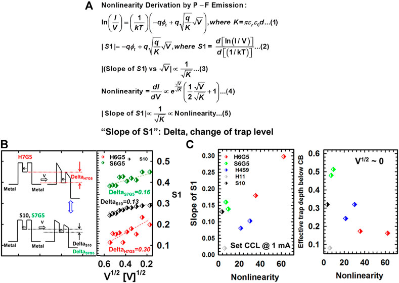
FIGURE 2. (A) Summary of internal filament gap design by Poole–Frenkel formula in (Park et al., 2013) DC response, where B is a constant, q is the elementary charge, φt is the energy barrier that must be overcome by the electron, ɛr is the relative permittivity of the RS medium, d is dielectric thickness, k is the Boltzmann constant, and T is temperature. Huang and Lee (2017); Liu et al. (2016) derived the procedure from Poole–Frenkel formula (Moon et al., 2018). Non-linearity definition and derivate procedure (Sharma et al., 2015). The relationship between Poole–Frenkel carrier transport and non-linearity, (B) band diagram of the trap fluctuation under low (e.g., 0.28 V), and high voltage (e.g., 0.8 V) with the slope of S1 current fitting results in H6G5, S6G5, and H11, (C) slope of S1 (left) and trap depth (right) as a function of non-linearity in five device structures (SET CCL at 1 mA).
Electric field increases and IVread increases as effective oxide thickness (EOT) decreases. Effective oxide thickness was calculated and compared between devices. The high-k integrated device, that is, H6G5, has a smaller EOT (∼1.24 nm) than S6G5 (∼6 nm) and higher band bending under the same applied voltage. In addition, the oxygen affinity of HfOx is larger than that of SiOx, that is, oxygen concentration is higher in HfOx, which relates to the Gibbs free energy of HfOx (∆G0 ∼ − 266, 435) and SiOx (∆G0 ∼ − 215,600) under the same atmospheric conditions with the spontaneous oxidation process. The high-k materials, as an oxygen exchange layer, have higher oxygen vacancy concentrations (Vo+) than low-k materials, which leads to higher IVread and NL. It is thought to suggest that the high-k layer integration is desired in the bilayer engineering for improving the NL, especially for higher I at Vread, as compared to the single low-k layer and low-k/low-k stacked devices.
Figure 3A,B shows the memory window and switching voltages as a function of graphite thickness, that is, 0, 3, 5, 8, and 10 nm with the identical thickness of HfOx (6 nm) in the stacked devices. The 30 devices of each graphite thickness were measured here for device-to-device (D2D) variation. As shown in Figure 3A, the memory window increased with the increasing graphite thickness, where the higher HRS current reduced ∼10X with thicker graphite, which is attributed to the improved thermal conductivity, that is, efficient joule heating in the RESET process. Meanwhile, the SET/RESET voltages are independent of the graphite thickness, which depicts the insulator layer that determines the switching voltages, that is, the high-k layer, as discussed in Figure 2. According to the high demands of computing and data storage, the multilevel cell applications in emerging memory become beneficial for brain-inspired computing, where the memory component is utilized as mimicking the synapses and neurons for the new computational architecture. Herein, the self-rectified memory is demonstrated with the multilevel states under the SET compliance current limit (CCL) modulation from 1 to 5 mA. Both the HRS and LRS are modulated by elevating the CCL. Note that the self-rectifying characteristic is optimized with the CCL of 1–3 mA and was compromised for high-memory window under higher CCL (3–5 mA).
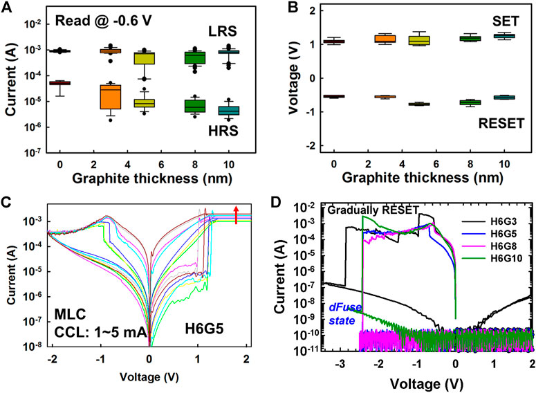
FIGURE 3. (A) Low resistance state (LRS) and high resistance state (HRS) for various graphite thickness, (B) SET and RESET voltage for various graphite thickness, (C) I-V characteristics with SET CCL modulations on H6G5, (D) dielectric fuse state for varied graphite thickness.
In addition, multi-programmable OTP is developed in this work based on the dielectric fuse breakdown (called “dFuse”) with the varied thickness of graphite (Figure 3D). The self-rectifying operational regime (i.e., RESET at −2.1 V in Figure 1A) enables users to recompile and revise data before storing information permanently. This shows the feature rewritable for the user before the final write state. While the write voltage of dFuse is applied (i.e., −2 to −3 V), the dielectric breakdown occurs and completes the fuse state at the lowest current level of ∼0.1 nA and cannot recover again. It is suggested that the dielectric breakdown occurs in HfOx thin-film breakdown as the electric field enhancement with the graphite layer acts as the interfacial conductive layer between the dielectric and bottom electrodes. Meanwhile, the thermal conductivity of graphite is 1,950 W/m-K (Jang et al., 2010), which is a good thermal sink for good reliability properties on the conductive filaments. The thicker graphite, for example, 5, 8, and 10 nm thickness, provides a superior thermal conduction path for the dielectric fuse breakdown, that is, “dFuse state,” with reducing voltage for lower power consumption. It is worthy to note that the devices performed as the self-rectifying RRAM with gradually RESET behaviors before dFuse voltage was applied, which is favorable for the multilevel application before the permanent program step.
In summary, the graphite-based RRAM devices with a self-rectifying characteristic, that is, non-linearity have been presented and demonstrated with MLC application as well as the dFuse state, which enables an OTP with the reprogrammable data storage before the permanent written-in process. The self-rectified RRAMs were proposed for the embedded integrated application according to its CMOS compatibility, low power consumption, excellent scalability for future emerging memory, and computing applications.
The raw data supporting the conclusion of this article will be made available by the authors, without undue reservation.
Y-CC outlined the concepts, discussed the sections, researched the literature for this review article, and wrote the text of the article.
The author declares that the research was conducted in the absence of any commercial or financial relationships that could be construed as a potential conflict of interest.
All claims expressed in this article are solely those of the authors and do not necessarily represent those of their affiliated organizations, or those of the publisher, the editors, and the reviewers. Any product that may be evaluated in this article, or claim that may be made by its manufacturer, is not guaranteed or endorsed by the publisher.
Chen, Y.-C., Hu, S.-T., Lin, C.-Y., Fowler, B., Huang, H.-C., Lin, C.-C., et al. (2018a). Graphite-Based Selectorless RRAM: Improvable Intrinsic Nonlinearity for Array Applications. Nanoscale. 10 (33), 15608–15614. doi:10.1039/c8nr04766a
Chen, Y. C., Lin, C. Y., Huang, H. C., Kim, S., Fowler, B., Chang, Y. F., et al. (2018b). Internal Filament Modulation in Low-Dielectric gap Design for Built-In Selector-Less Resistive Switching Memory Application. J. Phys. D: Appl. Phys. 51 (5), 055108. doi:10.1088/1361-6463/aaa1b9
Chen, Y. C., Huang, H. C., Lin, C. Y., Hu, S. T., Lin, C. C., and Lee, J. C. (2019a). Selectorless Resistive Switching Memory: Non-Uniform Dielectric Architecture and Seasoning Effect for Low Power Array Applications. AIP Adv. 9 (7), 075119. doi:10.1063/1.5097233
Chen, Y. C., Lin, C. C., Hu, S. T., Lin, C. Y., Fowler, B., and Lee, J. (2019b). A Novel Resistive Switching Identification Method Through Relaxation Characteristics for Sneak-Path-Constrained Selectorless RRAM Application. Sci. Rep. 9 (1), 12420. doi:10.1038/s41598-019-48932-5
Chen, Y. C., Lin, C. C., and Chang, Y. F. (2021). Post-moore Memory Technology: Sneak Path Current (Spc) Phenomena on Rram Crossbar Array and Solutions. Micromachines. 12 (1), 50. doi:10.3390/mi12010050
Chen, Z., Kulkarni, S. H., Dorgan, V. E., Rajarshi, S. M., Jiang, L., and Bhattacharya, U. (2017). A 0.9-μm² 1T1R Bit Cell in 14-nm High-Density Metal Fuse Technology for High-Volume Manufacturing and In-Field Programming. IEEE J. Solid-state Circuits. 52 (4), 933–939. doi:10.1109/jssc.2016.2641955
Cheng, H. W., Hsieh, E. R., Huang, Z. H., Chuang, C. H., Chen, C. H., Li, F. L., et al. (2018). “A Novel Rewritable One-Time-Programming OTP (RW-OTP) Realized by Dielectric-Fuse RRAM Devices Featuring Ultra-high Reliable Retention and Good Endurance for Embedded Applications,” in 2018 International Symposium on VLSI Technology, Systems and Application, VLSI-TSA 2018 (Institute of Electrical and Electronics Engineers Inc), 1–2. doi:10.1109/vlsi-tsa.2018.8403852
Doi, R., Yu, J., and Hashimoto, M. (2018). “Sneak Path Free Reconfiguration of Via-Switch Crossbars Based FPGA,” in IEEE/ACM International Conference on Computer-Aided Design, Digest of Technical Papers, ICCAD (Institute of Electrical and Electronics Engineers Inc). doi:10.1145/3240765.3240849
Doi, R., Yu, J., and Hashimoto, M. (2020). Sneak Path Free Reconfiguration With Minimized Programming Steps for Via-Switch Crossbar-Based FPGA. IEEE Trans. Comput.-Aided Des. Integr. Circuits Syst. 39 (10), 2572–2587. doi:10.1109/tcad.2019.2960331
Huang, Y. J., and Lee, S. C. (2017). Graphene/h-BN Heterostructures for Vertical Architecture of RRAM Design. Sci. Rep. 7 (1), 9679. doi:10.1038/s41598-017-08939-2
Jang, W., Chen, Z., Bao, W., Lau, C. N., and Dames, C. (2010). Thickness-Dependent Thermal Conductivity of Encased Graphene and Ultrathin Graphite. Nano Lett. 10 (10), 3909–3913. doi:10.1021/nl101613u
Ki Hong, S., Eun Kim, J., Kim, S. O., and Jin Cho, B. (2011). Analysis on Switching Mechanism of Graphene Oxide Resistive Memory Device. J. Appl. Phys. 110, 044506. doi:10.1063/1.3624947
Kulkarni, S. H., Ikram, U., Bhatt, K., Chao, Y.-L., Chang, Y.-F., Jenkins, I., et al. (2021). A 5-V-Program 1-V-Sense Anti-Fuse Technology Featuring On-Demand Sense and Integrated Power Delivery in a 22-nm Ultra Low Power FinFET Process. IEEE Solid-state Circuits Lett. 4, 2–5. doi:10.1109/lssc.2020.3041236
Lim, H., Sun, W., and Shin, H. (2016). ReRAM Crossbar Array: Reduction of Access Time by Reducing the Parasitic Capacitance of the Selector Device. IEEE Trans. Electron. Devices. 63 (2), 873–876. doi:10.1109/ted.2015.2506598
Liu, R., Barnaby, H. J., and Yu, S. (2016). System-level Analysis of Single Event Upset Susceptibility in RRAM Architectures. Semiconductor Sci. Technology. 31 (12), 31. doi:10.1088/0268-1242/31/12/124005
Liu, R., Wu, H., Pang, Y., Qian, H., and Yu, S. (2018). “Extending 1kb RRAM Array from Weak PUF to strong PUF by Employment of SHA Module,” in Proceedings of the 2017 Asian Hardware Oriented Security and Trust Symposium (AsianHOST 2017. Institute of Electrical and Electronics Engineers Inc), 67–72.
Moon, K., Fumarola, A., Sidler, S., Jang, J., Narayanan, P., Shelby, R. M., et al. (2018). Bidirectional Non-Filamentary RRAM as an Analog Neuromorphic Synapse, Part I: Al/Mo/Pr0.7Ca0.3MnO3 Material Improvements and Device Measurements. IEEE J. Electron. Devices Soc. 6 (1), 146–155. doi:10.1109/jeds.2017.2780275
Okuno, J., Kunihiro, T., Konishi, K., Maemura, H., Shute, Y., Sugaya, F., et al. (2020). “SoC Compatible 1 T1 C FeRAM Memory Array Based on Ferroelectric Hf0.5Zr0.5O2,” in 2020 IEEE Symposium on VLSI Technology, 1–2. doi:10.1109/vlsitechnology18217.2020.9265063
Park, S., Noh, J., Choo, M. L., Sheri, A. M., Chang, M., Kim, Y. B., et al. (2013). Nanoscale RRAM-Based Synaptic Electronics: Toward a Neuromorphic Computing Device. Nanotechnology. 24 (38), 384009. doi:10.1088/0957-4484/24/38/384009
Shamsoshoara, A., Korenda, A., Afghah, F., and Zeadally, S. (2020). A Survey on Physical Unclonable Function (PUF)-Based Security Solutions for Internet of Things. Computer Networks 183 (2020), 107593.
Sharma, A. A., Jackson, T. C., Schulaker, M., Kuo, C., Augustine, C., Bain, J. A., et al. (2015). “High Performance, Integrated 1T1R Oxide-based Oscillator: Stack Engineering for Low-Power Operation in Neural Network Applications,” in 2015 Symposium on VLSI Technology (VLSI Technology), Kyoto, Japan, June 16–18, 2015 (IEEE), T186–T187. doi:10.1109/VLSIT.2015.7223672
Sungho Kim, S., Jiantao Zhou, J., and Lu, W. D. (2014). Crossbar RRAM Arrays: Selector Device Requirements During Write Operation. IEEE Trans. Electron. Devices. 61 (8), 2820–2826. doi:10.1109/ted.2014.2327514
Yang, W. Y., Hsieh, E. R., Cheng, C. H., and Chung, S. S. (2020). “A Self-Align Gate-Last Resistive Gate Switching FinFET Nonvolatile Memory Feasible for Embedded Applications,” in 2020 IEEE Silicon Nanoelectronics Workshop, SNW 2020 (Institute of Electrical and Electronics Engineers Inc), 23–24. doi:10.1109/snw50361.2020.9131669
Keywords: selectorless, OTP, fuse, resistive random-access memory, self-rectify
Citation: Chen Y-C (2021) Self-Rectified Graphite-Based Reprogrammable One-Time Programmable (RS-OTP) Memory for Embedded Applications. Front. Nanotechnol. 3:772234. doi: 10.3389/fnano.2021.772234
Received: 07 September 2021; Accepted: 26 October 2021;
Published: 22 November 2021.
Edited by:
K. T. Varughese, Central Power Research Institute, IndiaReviewed by:
Yong Chen, University of South China, ChinaCopyright © 2021 Chen. This is an open-access article distributed under the terms of the Creative Commons Attribution License (CC BY). The use, distribution or reproduction in other forums is permitted, provided the original author(s) and the copyright owner(s) are credited and that the original publication in this journal is cited, in accordance with accepted academic practice. No use, distribution or reproduction is permitted which does not comply with these terms.
*Correspondence: Ying-Chen Chen, WWluZy1DaGVuLkNoZW5AbmF1LmVkdQ==
Disclaimer: All claims expressed in this article are solely those of the authors and do not necessarily represent those of their affiliated organizations, or those of the publisher, the editors and the reviewers. Any product that may be evaluated in this article or claim that may be made by its manufacturer is not guaranteed or endorsed by the publisher.
Research integrity at Frontiers
Learn more about the work of our research integrity team to safeguard the quality of each article we publish.