 Chuang Liu
 Yanping Wang*
- School of Information Science and Engineering, Dalian Polytechnic University, Dalian, China
With the development of new energy industries such as photovoltaics, microgrids, or distributed energy sources require many DC-AC grid-connected interfaces. Reducing the switching loss of the inverter is important to improve the transmission efficiency of the inverter, reduce the heat generation of the inverter, promote the high frequency and miniaturization of the inverter, and efficiently use the distributed energy. Therefore, considering the wide application of DC-AC power electronic interfaces in microgrid and distributed energy, and to make up for existing deficiencies in traditional hard-switching inverters, an optimal control strategy and topology for an optimal-auxiliary resonant commutated pole (O-ARCP) inverter is proposed in this article. Firstly, this paper introduces the proposed inverter topology and analyzes the operation mode of the circuit with the control strategy. Then simulation experiments in islanding mode are carried out to verify the rationality of the content, and finally simplified experimental verification is carried out based on the simulation results. Simulation and experimental testing reveal that all switches of the proposed topology are in soft-switching mode, which proves the effectiveness of the proposed control strategy and analysis. The analysis and validation of this paper provide assistance in the development of control strategies and structures for soft-switching inverters.
1 Introduction
The development of renewable energy can effectively reduce dependence on fossil fuels and environmental pollution. As a result, distributed energy sources such as photovoltaic power, wind power, and hydropower have been developing rapidly.
Many distributed energy sources can be efficiently arranged and managed when they are connected to a microgrid in a uniform manner. Therefore, the development of microgrids can help reduce carbon emissions, improve the utilization of clean energy, and solve the problem of local consumption of renewable energy. However, the large amount of distributed energy access requires more efficient power electronic interfaces, of which DC-AC power electronic converters are an important component. Further reducing the loss of the DC-AC converter and ensuring its efficient and stable operation is a key issue.
The conventional hard-switching inverter has a dramatic increase in switching losses as the pulse width modulation (PWM) frequency rises, and soft-switching techniques have been developed to reduce the losses caused by the increase in switching frequency (Zhang et al., 2010; Li and Xu, 2013; Mishima et al., 2013; Li, 2015; Pal A and Basu K. A, 2018; Samani et al., 2018).
The earliest soft-switching inverter is the resonant DC-link inverter proposed by Divan (1989), which was epoch-making for soft-switching inverter technology development. This topology is very simple, and only one set of LC devices is required to make the whole circuit work in soft-switching mode. However, it also has a very clear drawback: when resonance occurs, the DC bus voltage’s resonant peak is too high, significantly increasing the stress on the bus voltage. Active clamped resonant DC-link inverters are proposed to solve this problem. Moreover, many new solutions have been proposed in recent years for resonant losses and control techniques (Divan and Skibinski, 1989; Deshpande et al., 1997; Jafar and Fernandes, 2002; Gurunathan and Bhat, 2007; Amirabadi et al., 2014).
Some scholars have proposed a parallel resonant DC link inverter to replace the resonant DC link resonant inductor connected in series among the bus power, where the resonant inductor is connected in parallel among the power channels. This structure bus voltage stress is not higher than the DC voltage, and the inverter can use PWM modulation. However, frequent bus voltage over zero can affect the efficiency of soft switching (Chibani and Nakaoka, 1992; Hui et al., 1996; Chen, 1998; De Andrade et al., 2001; Behera et al., 2004; Pan and Luo, 2004; Pan and Luo, 2005; Mandrek and Chrzan, 2007; Kedarisetti and Mutschler, 2011; Wang et al., 2014).
The auxiliary resonant commutated pole (ARCP) inverter was proposed in 1989 with bus voltage not periodically resonating to zero. The auxiliary circuit only works at the moment of current change, with little loss to itself and low loss to the circuit. This approach is the best choice to achieve efficient soft switching under high power, but the voltage of the midpoint capacitor is not easy to stabilize due to the use of voltage-dividing capacitors. Subsequent scholars have proposed many improvement strategies.
Cai et al. (2019) proposed a novel ARCP inverter that achieved good results by replacing the position of the midpoint capacitor with a switching device.
Chu et al. (2014) and Chu et al. (2016) also utilized switching devices for current conversion, but too many auxiliary devices increase the losses.
Other studies (Yu et al., 2009; Chu et al., 2014; Chu et al., 2019; Wang and Wang, 2020; Chu et al., 2022) do not use a midpoint capacitor for current conversion, but their control strategy has an auxiliary circuit operating at both dead times within a single PWM cycle, which leads to an increase in losses.
The DC-AC power electronic converter interface assumes an important role in grid-connected or off-grid microgrids. The overall efficiency of the inverter cannot be improved due to the switching losses during the transmission of the DC-AC power electronic converter, and there are problems such as limited switching frequency, oversized filters, and heat generation. A new soft-switching topology of the auxiliary resonant commutation stage is proposed to address the switching losses in the transmission process of the grid-connected inverter. The control strategy and topology are simplified to address the complex control problem of the traditional soft-switching topology. The soft-switching process only occurs in the dead time of the inverter, and only half of the auxiliary switches are required to work every half cycle to make the inverter work in the soft-switching mode. Based on this topology, the switching losses of the grid-connected inverter can be reduced, the conversion efficiency of the inverter can be improved, and the inverter can be operated at a higher frequency to reduce the harmonics.
2 Materials and methods
2.1 Introduction to auxiliary circuits
The soft-switching topology is shown in Figure 1. One of the phases is used as a reference to analyze its operating principle, and its equivalent circuit diagram is shown in Figure 1B.
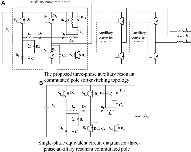
FIGURE 1. Topology schematic representation. (A) Three-phase circuit diagram; (B) single-phase equivalent schematic representation.
The auxiliary circuit consists of switching S1 and S4, resonant capacitors C1, C2, and C3, auxiliary diodes D5–D10, and resonant inductors L1–L4.
L1, D7, and C3 provide the ZCS turn-on condition for S2. C3 provides the ZVS turn-off condition for S2. L2 and C1 provide the ZCS turn-on and ZVS turn-off conditions for S1.
C3 and L3 provide the ZCS turn-on condition for S3. C3 provides the ZVS turn-off condition for S3. L4 and C2 provide the soft-switching condition for S4.
2.2 Basic working principle
To facilitate the analysis of the entire circuit structure, the article takes one of the three equivalent phases for analysis. The topological circuit divides the circuit into two time periods with positive and negative load current directions, respectively. Its switching equivalent control schematic representation and partial voltage and current are shown in Figure 2.
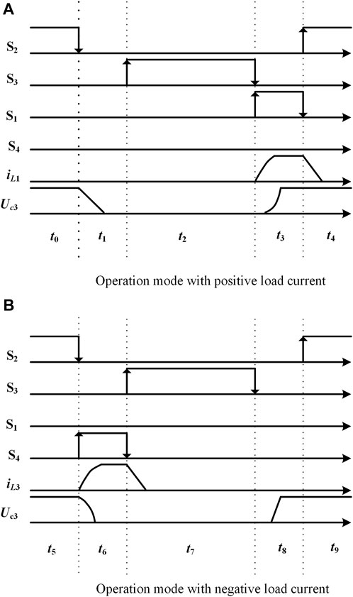
FIGURE 2. Switching control strategy and main waveforms for positive and negative load current directions. (A) Operation mode with positive load current; (B) Operation mode with negative load current.
Figure 2A includes the
Figure 2B includes the S1–S4 switching operation mode when the load current direction is negative during the t5–t9 time period, the change in inductor current iL flowing through the auxiliary inductor L3, and the change in voltage Uc3 across the auxiliary capacitor C3.
Where the signal is high level, S1–S4 represents the switch turn-on state; when the signal is low level, S1–S4 represents the turn-off state. For S2, S3, each drive interval has a certain dead time to turn on the auxiliary circuit to achieve the effect of soft switching.
As can be seen from Figure 2, under the control strategy proposed in this paper, only switch S1 is required to work when the load current direction is positive to achieve the soft-switching effect. Similarly, only switch S4 is required to work when the load current direction is negative. Compared with the control strategy proposed by Chu et al. (2016), the additional losses due to the need to turn on S1 and S4 alternately for each PWM cycle are greatly reduced. Compared to the control strategy in this paper, Chu et al. (2014) required multiple auxiliary switches to work alternately, which both complicates the control strategy and adds additional losses.
An analysis of the circuit yields the equivalent circuit diagram shown in Figure 3.
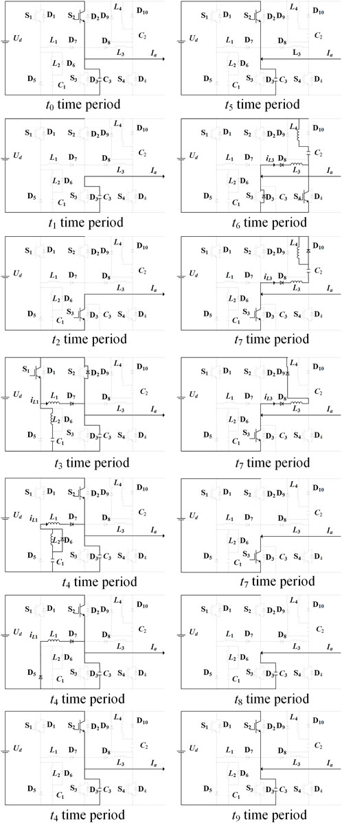
FIGURE 3. Equivalent circuits in different operating modes.
2.3 Operation mode with positive load current
When the load current direction is positive, the current mainly flows through switch S2 only when a group of auxiliary components corresponding to S1 is in working condition.
The operating mode is divided into five operating time periods, and, assuming it is in an ideal state, the principle of the circuit is analyzed as follows:
Mode t0: At this stage, switch S2 is turned on, the auxiliary circuit does not work, and the load current flows from switch S2 to the load.
Mode t1: Switch S3 is in the off state at this stage. When switch S2 needs to be turned off, the voltage across container C3 does not change suddenly, the magnitude of the voltage across capacitor C3 is still the bus voltage, and the UC3 voltage drops to zero after a period of time. The voltage across switch S2 is zero. Therefore, switch S2 is the ZVS turn-off. When switch S2 needs to be turned on, the auxiliary circuit needs to work to provide the ZVS turn-on condition for S2.
At this time, the voltage across Uc3 decreases linearly, as shown in the following equation:
where Ud is the busbar voltage.
Mode t2: S3 is turned on at this stage. Because the capacitive voltage across Uc3 has been reduced to zero in mode t1, S3 is the ZVS turn-on.
Mode t3: S1 turns on, and the resonant current iL1 begins to rise nonlinearly. Because L1 and L2 will obstruct the instantaneous current, the auxiliary switch S1 is the ZCS turn-on. When the resonant current reaches the value of the load current, the resonant current iL1 is in the constant current stage. The voltage at both ends of capacitor Uc3 starts to rise. When it reaches the bus voltage, diode D2 conducts, so S2 is the ZVS turn-on. At the same time, part of the current flows through L2 and C1, and the voltage across C1 begins to rise in preparation for the ZVS turn-off of S1.
The relevant changes are analyzed as shown in the following equations. The current iL1 flowing through L1 is shown in the following equation:
The current iL2 flowing through L2 is analyzed as shown in the following equation:
The maximum current Is1max flowing through S1 is shown in the following equation:
The change in voltage across C1, C3 is shown in the following equation:
where
Mode t4: When the voltage across C1 reaches the bus voltage, the voltage across C1 does not rise due to the clamp effect of diode D6. When S1 needs to be turned off, the voltage across S1 is zero due to the presence of capacitor C1. Therefore, the S1 turn-off belongs to the ZVS turn-off. When S1 is turned off, the resonant current iL1 decreases at a linear rate.
2.4 Operation mode with negative load current
When the load current direction is negative, it is divided into five action time zones according to the action time sequence, and, assuming that the circuit is in an ideal state, the corresponding time range in Figures 2, 3 is the t5–t9 time period, which is analyzed as follows.
Mode t5: At this time, switch S2 remains on, but the load current direction is negative.
Mode t6: S4 turns on, and the resonant current iL3 begins to rise nonlinearly. Because L3 and L4 will obstruct the instantaneous current, the auxiliary switch S4 is the ZCS turn-on. The capacitance voltage Uc3 begins to decrease until the D3 begins to conduct. At this time, the capacitance voltage across C2 begins to rise in preparation for the ZVS turn-off of S4.
At this time, the current iL3 flowing through the inductor L3 changes, as shown in the following equation:
The current iL4 flowing through inductor L4 changes as shown in the following equation:
The current Is4 flowing through switch S4 changes as shown in the following equation:
The voltage across the capacitor C3 changes as shown in the following equation:
Here,
Mode t7: At this time, the S3 anti-parallel diode has been on, and the switch S3 should be turned on at this time. Therefore, the switch S3 is the ZVS turn-on. Because the voltage at both ends of C2 is the bus voltage, the voltage at both ends of switch S4 is zero, and S4 meets the condition of the ZVS turn-off. With the closing of S4, the energy stored in C2, L3, and L4 is released back to the bus.
Mode t8: When the switch S3 turns off, the voltage across the capacitor C3 cannot change abruptly. Therefore, switch S3 reaches the condition for the ZVS turn-off.
Mode t9: Because C2 has stored enough energy before S2 turns on, the voltage across S2 is zero to meet the condition of the ZVS turn-on. Then, S2 turns on and enters a new cycle.
3 Simulation data and analysis of an O-ARCP DC-AC power electronic converter in islanding mode
To verify the correctness of the analysis, the proposed three-phase ARCP inverter topology is simulated using MATLAB simulation software. Because some parameters of the three-phase circuit are the same, only one-phase parameters are listed.
The simulation parameters are shown in Table 1.
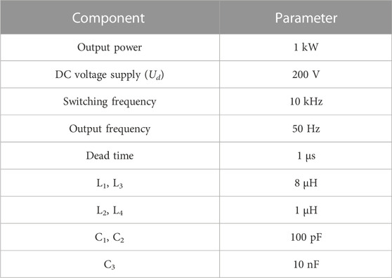
TABLE 1. Simulation parameters of the three-phase ARCP inverter.
3.1 Parameter design when the load current direction is positive
3.1.1 Design of resonant inductor and resonant capacitor
The design of the
Namely,
The equation can be rewritten as follows:
where K > 1, and the resonance duration period is defined by
The auxiliary switch opening time cannot be less than t. t can be determined by the following equation:
Meanwhile, the duration of t should satisfy
where
Combining the aforementioned equations yields
where K1 < 1. It can be concluded that
where K1 < 1 and K > 1.
3.1.2 Parameter design of C1, L2
This phase has a small resonance duration, so only t1 < t needs to be satisfied.
Its peak resonant current can be given by
The design should satisfy iL2 < iL1 in order to reduce losses and current stress.
Therefore, it is obtained that
where K2 < 1 and K3 < 1.
To simplify the design, iL1 can be simplified. This yields
3.2 Parameter design when the load current direction is negative
The analysis process is the same as when the load current direction is positive.
3.3 Simulation verification
The output three-phase voltage and its harmonic analysis are shown in Figure 4.
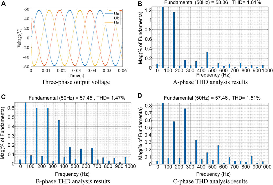
FIGURE 4. Output three-phase voltage waveform and THD analysis results. (A) Three-phase output voltage; (B) A-phase THD analysis results; (C) B-phase THD analysis results; (D) C-phase THD analysis results.
Figure 4A shows the output three-phase voltages, Figure 4B shows the results of the A-phase total harmonic distortion (THD) analysis with a value size of 1.61%, Figure 4C shows the results of the B-phase THD analysis with a value size of 1.47%, and Figure 4D shows the results of the C-phase THD analysis with a value size of 1.51%, which is not significantly different from the experimental tests in Section 4 and meets the design expectations.
Figure 5 shows the simulation diagram of the operation mode with positive load current direction, where the first picture shows the current and voltage waveforms on the switch side of S2, the second picture shows the current flowing through inductor L1, and the third picture shows the driving pulse of auxiliary switch S1.
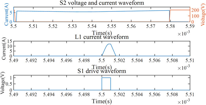
FIGURE 5. Key waveform with a positive load current direction.
A comparison with Figure 2 shows that the proposed topology achieves the desired soft-switching effect in the simulation verification.
Figure 6 shows the simulation diagram of the operation mode with negative load current direction, where the first picture shows the current and voltage waveforms on the switch side of S3, the second picture shows the current flowing through inductor L2, and the third picture shows the driving pulse of auxiliary switch S4. The comparison with Figure 2 is consistent with the analysis, and the desired soft-switching effect is achieved.
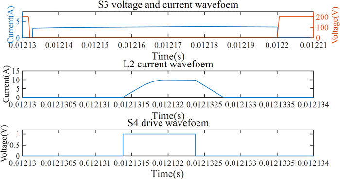
FIGURE 6. Key waveform with a negative load current direction.
The first graph in Figure 7 shows the turn-off waveform of auxiliary switch S1 in the operation mode with a positive load current direction. The second graph shows the turn-off waveform of auxiliary switch S4 in the operation mode with a negative load current direction. It can be seen that the proposed topology can satisfy the ZVS turn-off of the auxiliary switch and reduce the switching loss.
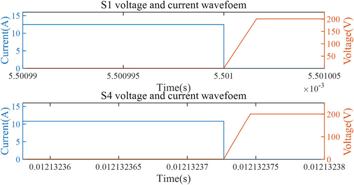
FIGURE 7. Auxiliary switch off waveform with positive and negative load current directions.
4 Experimental verification and analysis
Experimental verification was carried out to verify the correctness of the simulation strategy. In this verification, the parameters of the three-phase circuit were partially consistent, so only one-phase parameters are listed. The simulation parameters are shown in Table 2.
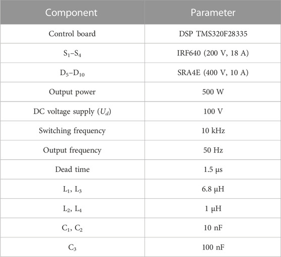
TABLE 2. Experimental parameters.
Figure 8 shows the hardware experimental platform of the proposed O-ARCP converter, including the basic circuits such as the main circuit, the auxiliary converter circuit, the filter, the main control circuit, and the driver circuit.
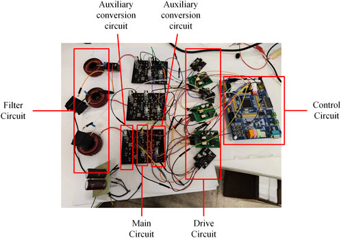
FIGURE 8. Experimental hardware platform.
Figure 9 shows the output three-phase voltage waveform.
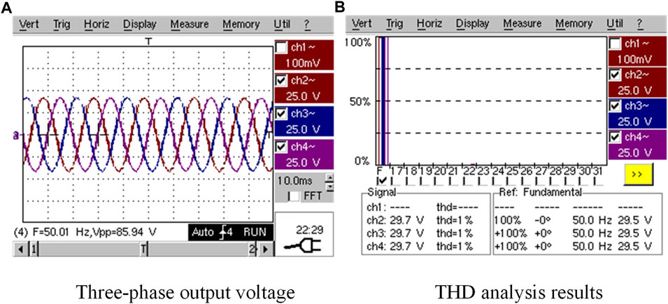
FIGURE 9. Three-phase voltage output and THD analysis results. (A) Three-phase output voltage; (B) THD analysis results.
Figure 9A shows the inverter output three-phase voltage, and Figure 9B shows the inverter THD analysis results. From Figure 9A, we can see that the inverter output voltage waveform Vpp is 85.94 V, and the frequency is 50.01 HZ. As can be seen from Figure 9B, the THD analysis results for all three channels are 1% and meet the design criteria. The experimental results do not have large errors with the simulation results.
Figure 10 shows the experimental graph of the ZVS turn-on and the ZVS turn-off waveform.
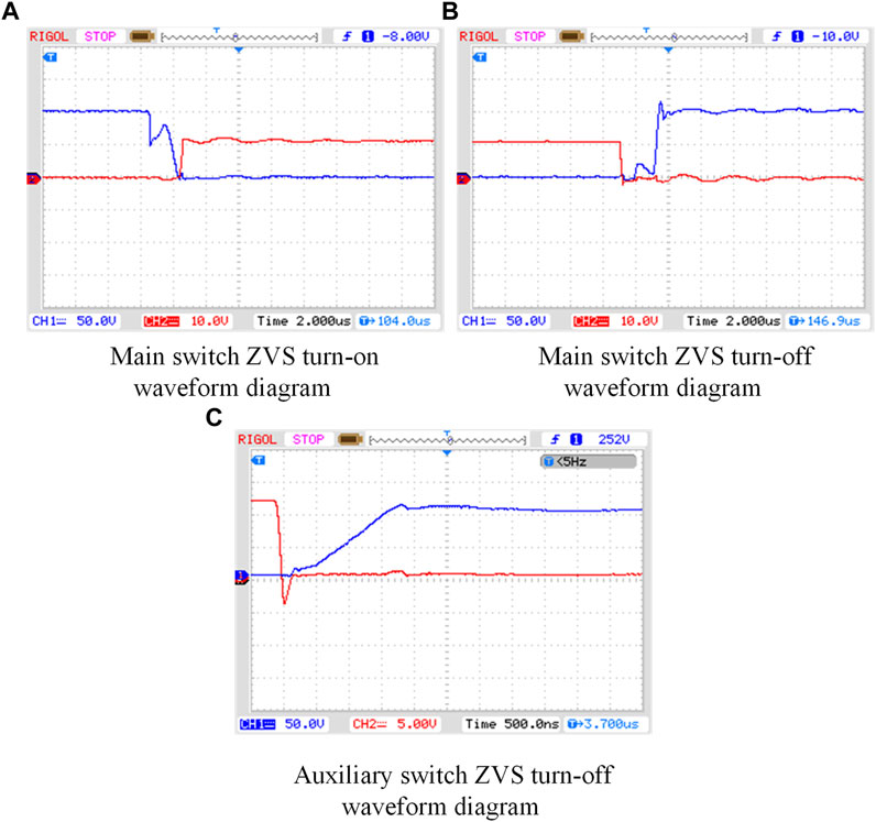
FIGURE 10. Experimental waveforms on both sides of the main and auxiliary switches. (A) Main switch ZVS turn-on waveform diagram; (B) Main switch ZVS turn-off waveform diagram; (C) Auxiliary switch ZVS turn-off waveform diagram.
Figure 10A shows the waveform diagram of the main switch ZVS turn-on moment, Figure 10B shows the waveform diagram of the main switch ZVS turn-off moment, and Figure 10C shows the waveform diagram of the auxiliary switch ZVS turn-off moment. The red lines represent the main switch drive signals, and the blue lines represent the voltage signals at both ends of the main switch.
It can be observed in Figure 10A that the voltage at both ends has changed to zero before the main switch is turned on. Therefore, the main switch meets the condition of the ZVS turn-on. In Figure 10B, after the main switch is turned off, the voltage at both ends is zero and rises slowly to the bus voltage after a period of time. Therefore, the main switch meets the condition of the ZVS turn-off. In Figure 10C, when the auxiliary switch is turned off, the voltage across the auxiliary switch is zero after taking approximately 2 μs to reach the bus voltage. Therefore, the auxiliary switch meets the conditions for the ZVS turn-off.
5 Comparison and analysis of inverters
5.1 Comparison of the number of devices used
Table 3 compares the number of components used in the auxiliary circuit.
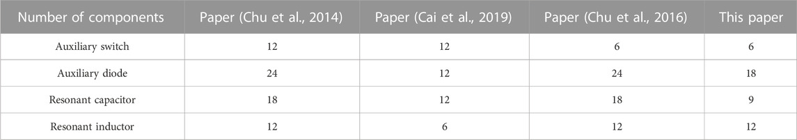
TABLE 3. Comparison of the number of auxiliary components.
Under the control strategy proposed in this paper, only half of the components are working in each sine wave cycle on average, so in practice, three auxiliary switches are working in each cycle, in addition to nine auxiliary diodes, five resonant capacitors, and six resonant inductors. The two groups of devices work alternately within the whole cycle, reducing the loss of the auxiliary circuit.
5.2 Comparative analysis of control strategies used
Figure 11 shows a comparison of the auxiliary switch control strategy described by Chu et al. (2016) and this paper. It can be seen from Fig. 11A that Chu et al. (2016) do not divide the action of the auxiliary switch into two moments according to the load current direction, and it is necessary to operate both switches S1 and S4 in one PWM cycle. In this paper, the control strategy is divided into two types according to the load current flow direction. Only the auxiliary switch S1 needs to be operated in each PWM cycle when the load current direction is positive, and only the auxiliary switch S4 needs to be operated in each PWM cycle when the load current direction is negative, thus avoiding the problem of operating both auxiliary switches S1 and S4 in each PWM cycle. The control strategy described by Chu et al. (2016) is longer than the one proposed in this paper by one δt2 and one δt4, and the losses generated by the auxiliary circuit in this control strategy are larger than those in this paper.
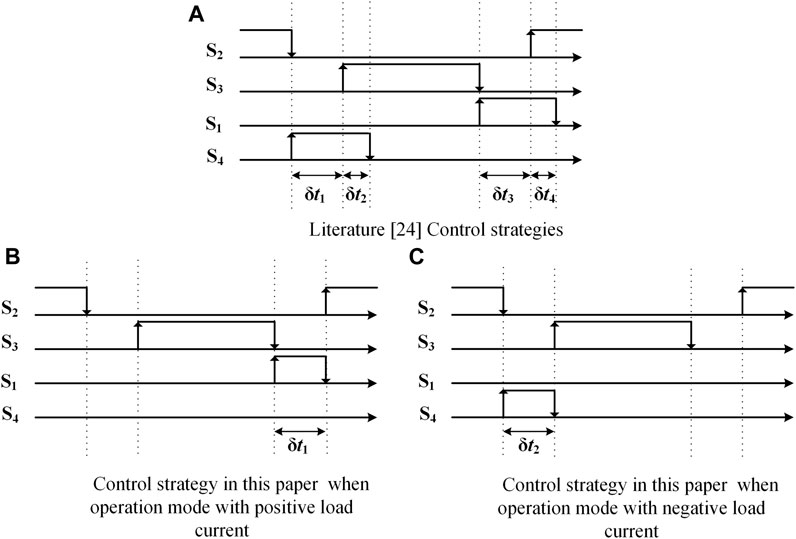
FIGURE 11. Control strategy comparison analysis chart. (A) Literature [24] Control strategies; (B) Control strategy in this paper when operation mode with positive load current; (C) Control strategy in this paper when operation mode with negative load current.
5.3 Efficiency comparison and analysis
Figure 12 shows the experimental efficiency curve of the proposed soft-switching inverter. When the output power is less than 300 W, both the soft-switching inverter proposed in this paper and the soft-switching inverter proposed by Chu et al. (2014) have less efficiency than the conventional hard-switched inverter. The reason is that the added auxiliary circuit generates more losses than the switching losses generated by the conventional hard-switched inverter.
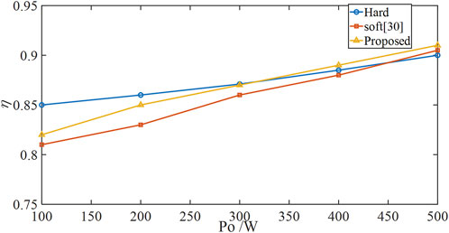
FIGURE 12. Efficiency comparison chart.
When the output power is greater than 300 W, the efficiency of the soft-switching inverter proposed in this paper starts to be greater than that of the conventional hard-switched inverter. In contrast, the soft-switching inverter described by Chu et al. (2014) is still smaller than the conventional hard-switched inverter.
The main reason for this effect is that the number of auxiliary devices used in this article is less than that described by Chu et al. (2014). Therefore, the losses generated by the auxiliary circuits are smaller. The second reason is that the auxiliary switching control strategy used by Chu et al. (2014) is similar to that described by Chu et al. (2016). The control strategy in this paper has a relatively short operating time of the auxiliary circuit. As a result, fewer additional power losses are incurred.
6 Conclusion
An efficient soft-switching topology is proposed in this paper, and after theoretical analysis and simulation experiments, the following conclusions are drawn.
1. Compared with the control strategies proposed in the literature (Chu et al., 2014; Chu et al., 2016), under the control strategy proposed in this paper, only one set of auxiliary components is under operation in every half cycle, and the auxiliary components work only once in a cycle, which greatly reduces the losses due to the auxiliary circuit.
2. Compared with Chu et al. (2014), the proposed topology in this paper reduces the number of auxiliary components used and reduces the size and cost of the inverter.
3. It is verified by simulation and experiment that the transmission efficiency of the grid-connected inverter can be improved in grid-connected or islanded mode.
Data availability statement
The original contributions presented in the study are included in the article/Supplementary material; further inquiries can be directed to the corresponding author.
Author contributions
CL and YW developed the idea. CL developed the theory, the calculations, and the simulations. YW supervised and reviewed this work. All authors contributed to the article and approved the submitted version.
Funding
The authors acknowledge financial support from the Natural Science Foundation of the Educational Department of Liaoning Province (Grant: J2020053) and the Technology Innovation Fund (Grant: 2020JJ26GX029), and would like to express many thanks for the support of the Dalian Key Laboratory of Smart Micro-grid and Green Recycling Industry. This work was supported by Dalian Polytechnic University.
Acknowledgments
The author is also very grateful to their mentor for his help.
Conflict of interest
The authors declare that the research was conducted in the absence of any commercial or financial relationships that could be construed as a potential conflict of interest.
Publisher’s note
All claims expressed in this article are solely those of the authors and do not necessarily represent those of their affiliated organizations, or those of the publisher, the editors, and the reviewers. Any product that may be evaluated in this article, or claim that may be made by its manufacturer, is not guaranteed or endorsed by the publisher.
References
Amirabadi, M., Baek, J., and Toliyat, H. A. (2014). Bidirectional soft-switching series AC-link inverter. IEEE Trans. Industry Appl. 51 (3), 2312–2320. doi:10.1109/tia.2014.2362963
Behera, S., Das, S. P., and Doradla, S. R. (2004). Quasi-resonant soft-switching inverter for low and high power factor loads. IEE Proceedings-Electric Power Appl. 151 (4), 451–459. doi:10.1049/ip-epa:20040355
Cai, M., Wasynczuk, O., and Saeedifard, M. (2019). A voltage-edge-rate-limiting soft-switching inverter based on auxiliary resonant pole. IEEE J. Emerg. Sel. Top. Power Electron. 7 (2), 736–744. doi:10.1109/jestpe.2019.2898890
Chen, Y. T. (1998). A new quasi-parallel resonant DC link for soft-switching PWM inverters. IEEE Trans. power Electron. 13 (3), 427–435. doi:10.1109/63.668102
Chibani, A., and Nakaoka, M. (October 1992). A new state-feedback control based 3 phase PWM inverter with improved parallel resonant DC link, Proceedings of the Conference record of the 1992 IEEE Industry applications society annual meeting. Houston, TX, USA. IEEE, 801–808.
Chu, E., Chen, Z., Xie, H., and Zhang, H. (2019). Modified double auxiliary resonant commutated pole inverter and its modulation strategy. IEEE J. Emerg. Sel. Top. Power Electron. 8 (4), 4467–4481. doi:10.1109/jestpe.2019.2939168
Chu, E., Wu, M., Huang, L., Hou, X., and Zhang, H. (2014). Research on a novel modulation strategy for auxiliary resonant commutated pole inverter with the smallest loss in auxiliary commutation circuits. IEEE Trans. Power Electron. 29 (3), 1103–1117. doi:10.1109/TPEL.2013.2261092
Chu, E., Zhang, T., and Wang, Z. (2022). Auxiliary resonant commutated pole soft-switching inverter with simple topology. J. Power Electron. 22 (2), 198–209. doi:10.1007/s43236-021-00352-3
Chu, E., Zhang, X., Sun, Q., Li, S., Xiong, H., and Yang, X. (2016). Three-phase double auxiliary resonant commutated pole inverter topology and analysis of its working principle. IET Power Electron. 9 (7), 1536–1545. doi:10.1049/iet-pel.2015.0393
De Andrade, D. A., Neto, R. M. F., de Freitas, L. C., Vieira, J., and Farias, V. (2001). A soft-switched current-controlled converter for induction machine drives. IEEE Trans. Power Electron. 16 (1), 64–71. doi:10.1109/63.903990
Deshpande, V. V., Doradla, S. R., and Divan, D. M. (1997). A current-prediction scheme for the PRDCL inverter-fed induction motor drive. IEEE Trans. power Electron. 12 (1), 64–71. doi:10.1109/63.554170
Divan, D. M., and Skibinski, G. (1989). Zero-switching-loss inverters for high-power applications. IEEE Trans. industry Appl. 25 (4), 634–643. doi:10.1109/28.31240
Divan, D. M. (1989). The resonant DC link converter-a new concept in static power conversion. IEEE Trans. Industry Appl. 25 (2), 317–325. doi:10.1109/28.25548
Gurunathan, R., and Bhat, A. K. S. (2007). Zero-voltage switching DC link single-phase pulsewidth-modulated voltage source inverter. IEEE Trans. power Electron. 22 (5), 1610–1618. doi:10.1109/tpel.2007.904169
Hui, S. Y. R., Gogani, E. S., and Zhang, J. (1996). Analysis of a quasi-resonant circuit for soft-switched inverters. IEEE Trans. power Electron. 11 (1), 106–114. doi:10.1109/63.484423
Jafar, J. J., and Fernandes, B. G. (2002). A new quasi-resonant DC-link PWM inverter using single switch for soft switching. IEEE Trans. Power Electron. 17 (6), 1010–1016. doi:10.1109/tpel.2002.805598
Kedarisetti, J., and Mutschler, P. (2011). A motor-friendly quasi-resonant DC-link inverter with lossless variable zero-voltage duration. IEEE Trans. power Electron. 27 (5), 2613–2622. doi:10.1109/tpel.2011.2174382
Li, R., and Xu, D. (2013). A zero-voltage switching three-phase inverter. IEEE Trans. Power Electron. 29 (3), 1200–1210. doi:10.1109/TPEL.2013.2260871
Li, Y. F. (2015). Active zero voltage switching tracking controller design for class E inverter to counteract the resonant components shifting. IET Power Electron. 8 (10), 2016–2025. doi:10.1049/iet-pel.2014.0310
Mandrek, S., and Chrzan, P. J. (2007). Quasi-resonant DC-link inverter with a reduced number of active elements. IEEE Trans. Industrial Electron. 54 (4), 2088–2094. doi:10.1109/tie.2007.895143
Mishima, T., Takami, C., and Nakaoka, M. (2013). A new current phasor-controlled ZVS twin half-bridge high-frequency resonant inverter for induction heating. IEEE Trans. Industrial Electron. 61 (5), 2531–2545. doi:10.1109/tie.2013.2274420
Pal A, Basu K. A, (2018). A soft-switched high-frequency link single-stage three-phase inverter for grid integration of utility scale renewables. IEEE Trans. Power Electron. 34 (9), 8513–8527. doi:10.1109/tpel.2018.2889795
Pan, Z. Y., and Luo, F. L. (2004). Novel soft-switching inverter for brushless DC motor variable speed drive system. IEEE Trans. Power Electron. 19 (2), 280–288. doi:10.1109/tpel.2003.823173
Pan, Z. Y., and Luo, F. L. (2005). Transformer based resonant DC link inverter for brushless DC motor drive system. IEEE Trans. power Electron. 20 (4), 939–947. doi:10.1109/tpel.2005.850972
Samani, R., Beyragh, D. S., and Pahlevani, M. (2018). A new grid-connected DC/AC inverter with soft switching and low current ripple. IEEE Trans. Power Electron. 34 (5), 4480–4496. doi:10.1109/tpel.2018.2863183
Wang, C. M., Lin, C. H., Lin, H. Y., and Hsu, S. (2014). Analysis, design and performance of a soft-switching single-phase inverter. IET Power Electron. 7 (9), 2412–2423. doi:10.1049/iet-pel.2013.0514
Wang, Q., and Wang, Y. (2020). Research on a novel high-efficiency three-phase resonant pole soft-switching inverter. IEEE Trans. Power Electron. 36 (5), 5845–5857. doi:10.1109/tpel.2020.3029186
Yu, W., Lai, J. S., Park, S. Y., Yang, L., Li, G., Li, H., et al. (2009). Effect of microwave irradiation on TATB explosive. IEEE Trans. Power Electron. 25 (4), 952–954. doi:10.1016/j.jhazmat.2009.02.124
Keywords: inverter, auxiliary resonant commutated pole, soft switching, zero voltage switching, zero current switching
Citation: Liu C and Wang Y (2023) Topology and control strategy optimization of an auxiliary resonant commutated pole-based, soft-switching grid-connected inverter. Front. Energy Res. 11:1200550. doi: 10.3389/fenrg.2023.1200550
Received: 05 April 2023; Accepted: 05 September 2023;
Published: 25 September 2023.
Edited by:
Jingyang Fang, Shandong University, ChinaReviewed by:
Qinglei Bu, Xi’an Jiaotong-Liverpool University, ChinaDehao Qin, Clemson University, United States
Copyright © 2023 Liu and Wang. This is an open-access article distributed under the terms of the Creative Commons Attribution License (CC BY). The use, distribution or reproduction in other forums is permitted, provided the original author(s) and the copyright owner(s) are credited and that the original publication in this journal is cited, in accordance with accepted academic practice. No use, distribution or reproduction is permitted which does not comply with these terms.
*Correspondence: Yanping Wang, d2FuZ3lwQGRscHUuZWR1LmNu