 Baiyi Liu
- 1Shanghai Jiao Tong University, Shanghai, China
- 2Ginlong Technologies Co., Ltd., Ningbo, China
The electromagnetic interference (EMI) is a key issue for most of electric or electronic devices, the researches of suitable analysis methods and solutions absorb much attentions. The research about electromagnetic interference (EMI) is normally based on two approaches (i.e., time domain analysis and frequency domain analysis). The frequency domain analysis is easier to apply theoretical model to analyze the circuit loop impedance of EMI noise which can provide guidance of EMI suppression, but it cannot reflect the real amplitude of EMI noise without the real waveforms of noise sources. The time domain analysis is usually based on circuit simulation to get the EMI noise directly, but it is time consuming. In order to combine the advantages of these two approaches, this paper proposes a high frequency equivalent circuit model of flyback converter and analyze the effect of each distributed parameters on the common mode (CM) and differential mode (DM) noise. The experimental result verified the accuracy and efficiency of the proposed method, which not only can correctly reflect the real waveforms of the circuit, but also can predict the EMI noise based on the constructed waveforms.
1 Introduction
In switch-mode power supplies (SMPS), to realize high power density design of power converters, the distance between components should be reduced which could strengthen the electromagnetic field coupling among the components, making the EMI issues more prominent. Therefore, effectively analyzing the mechanisms of EMI noise and proposing corresponding effective solutions are crucial for achieving high power density designs in SMPS.
The essential reason of EMI noise arises from the voltage transitions and current ripples induced by switching actions of the power converters. Consequently, constructing the switching waveforms of the main components in the power converters can effectively reflect the characteristics of the EMI noises. However, since the impact of EMI noises span high frequency bands, various distributed parameters of the circuit significantly influence the switching waveforms, rendering the corresponding differential equations exceedingly complex. As a result, current theoretical analyses of EMI noise are typically based on frequency domain analysis. Time domain analysis is mainly based on circuit simulation, but building and debugging a circuit simulation system has certain complexities. Therefore, it is of great significance to construct time-domain waveforms theoretically to analyze and predict EMI noise (Trinchero et al., 2015; Yang et al., 2020; Fu, 2019; Zhu et al., 2020; Takahashi et al., 2019; Ma et al., 2008; Liu et al., 2015; Emami et al., 2010; Kai et al., 2024; Fakhafkh and Ammous, 2017; Wang et al., 2012; Liang et al., 2012).
This paper utilizes the flyback converter as a platform, and based on its high frequency equivalent circuit model, provides a detailed analysis and solution of the differential equations corresponding to each switching process. This establishes the theoretical solution model for the switching waveforms in the flyback circuit. Building upon this foundation, this paper thoroughly examines the impact of various distributed parameters of the flyback circuit on the waveforms of different components, thereby deducing their influence on EMI noises (differential mode and common mode noises). Finally, through experimental verification, it is confirmed that the theoretically constructed switching waveforms of the flyback converter are highly accurate and can be effectively used to analyze the impact of distributed parameters on EMI noises.
2 EMI noise mechanisms of flyback circuit
When analyzing EMI noise in switch-mode power supply circuits, it is common to categorize the noise into differential mode and common mode components due to their distinct causes and transmission paths. Differential mode noise primarily originates from current ripples in the power loop of the circuits, thus its main transmission path lies between the line L and line N within the power loop. The DM noise transmission path of the flyback circuit is illustrated in Figure 1. Common mode noise, on the other hand, mainly arises from potential jumps during the switching process, leading to ground displacement currents. Therefore, its transmission path involves the loops between the line L and ground, as well as the line N and ground. In a flyback circuit, both the MOSFET of primary side and the diode of secondary side experience potential jumps during the switching instant, which can generate common mode noise. Figures 2, 3 show the transmission path of common-mode noise generated from the primary side and secondary side separately.
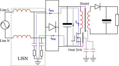
Figure 1. The differential-mode noise transmission path of the flyback circuit.
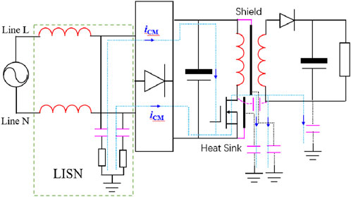
Figure 2. The primary side’s common-mode noise transmission path of the flyback circuit.

Figure 3. The secondary side’s common-mode noise transmission path of the flyback circuit.
Based on the noise transmission paths shown in Figures 1–3, one can intuitively analyze the impact of circuit’s distributed parameters on EMI noise propagation in the frequency domain. However, this method only reflects the effect of distributed parameters on noise within a given frequency band. In the absence of the original noise’s spectral information, this approach is suitable for qualitatively analyzing the impact of distributed parameters on EMI noise but does not facilitate predictive analysis of EMI during the design process of switch-mode power supplies. Generally, the waveforms at various points in the circuit are obtained via simulation and used for EMI prediction and design. However, constructing a waveform model that considers distributed parameters through circuit theory would be more beneficial for an in-depth analysis of these parameters' impact on EMI. Therefore, this paper will analyze the influence of distributed parameters on EMI noise sources by theoretically constructing the switching waveforms of the flyback circuit.
3 Theoretical model of flyback circuit waveforms
To construct relatively accurate switching waveforms for the flyback circuit, it is necessary to fully consider the effects of distributed parameters. For this purpose, the high-frequency equivalent circuit of the flyback transformer shown in Figure 4 is adopted in this paper. This circuit not only takes into account the leakage inductance, parasitic capacitance, excitation inductance, winding resistance, and core equivalent resistance, but also considers the impact of the parasitic capacitance of the primary side switch and the secondary side diode. This approach can more comprehensively reflect the influence of distributed parameters on the switching waveforms. Due to the majority of current mainstream flyback power supplies operate in DCM (Discontinuous Conduction Mode), which is in order to reduce winding losses and improve efficiency, this paper will use DCM as an example. Based on Figure 4, we will conduct a detailed analysis and construct the switching waveforms corresponding to each switching process.
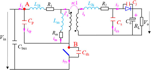
Figure 4. High frequency equivalent circuit model of flyback.
3.1 The waveforms of flyback circuit at turn off moment
At the turn-off moment of the flyback circuit, the primary switch is turned off and the secondary diode conducts (with a voltage drop VD). The voltage of the magnetizing inductance Lm is clamped by the output voltage, causing resonance between the primary leakage inductance Lk1, the primary capacitance Cp, and the switch’s drain-source capacitance Cds, as shown in Figure 5 which represents the equivalent circuit during the turn-off period of the flyback circuit. Based on Figure 5, the Equation 1 for the turn-off moment can be derived. In solving for the magnetizing inductance voltage VLm_off1(t), the influence of the secondary side resistance R2 and the magnetizing resistance Rm is neglected, assuming that the magnetizing current decreases linearly at this time.
Figure 5. The equivalent circuit of flyback circuit at the turn off moment.
By applying the Laplace transform to solve Equation 1, the time-domain equations for the switch capacitance voltage and magnetizing current at the turn-off moment can be obtained. Substituting these into Equation 2 allows further solution of the key circuit waveforms.
It is important to note that to completely solve Equation 1, the initial values of the switch junction capacitance voltage, the current through the switch, and the magnetizing current must be determined. At the turn-off moment, the current through the switch instantaneously transfers to the secondary side for “freewheeling,” meaning the magnetizing current remains constant (reaching its peak value Ipeak) and the switch current becomes zero. The voltage across the switch junction capacitance Cds) cannot change instantaneously and remains at zero. Therefore, at the turn-off moment, the initial values of the switch junction capacitance voltage, the current through the switch, and the magnetizing current satisfy Equation 3.
It should be noted that the oscillation frequencies corresponding to each switching process are different. Since resistance is frequency-dependent, a fixed resistance value cannot represent the actual winding resistance (such as R1 and R2) or core equivalent resistance (such as Rm) for each process. These values need to be estimated based on the oscillation frequency. At the turn-off moment, the resonance frequency of the primary circuit can be estimated using Equation 4. These resistances mainly act as damping during the LC resonance process. As long as their values do not affect the nature of the resonance (such as underdamped, critically damped, and overdamped resonance), they will not impact the analysis of the influence of other distributed parameters (such as transformer leakage inductance and parasitic capacitance) on the switch waveform. Therefore, the estimated value range for these resistances can be quite broad.
3.2 The waveforms of flyback circuit at discontinuous interval
During the discontinuous conduction period of the flyback circuit, the secondary side diode turns off, and the magnetizing inductance is no longer clamped by the output voltage. Instead, it participates in the resonance of the primary side circuit along with the primary leakage inductance L1k, the primary winding capacitance Cp, and the switch drain-source capacitance Cds. The resonant frequency can be calculated using Equation 5. As shown in Figure 6, the equivalent circuit during the discontinuous conduction period can be used to derive the corresponding circuit equations, as given in Equation 6. When the freewheeling time toff of the secondary side diode is determined, the initial values of the voltages and currents across the switch and the secondary winding during this period satisfy Equation 7.
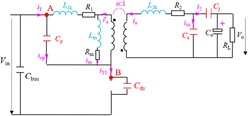
Figure 6. The equivalent circuit of flyback circuit at discontinuous interval.
Using the Laplace transform to solve Equation 6, the time-domain equations for the voltages across the switch and the secondary winding during the discontinuous conduction period can be obtained. Substituting these time-domain equations into Equation 8 allows the key waveforms of the circuit during the discontinuous conduction period to be determined.
3.3 The waveforms of flyback circuit at turn on moment
During turn on moment, the switch can be approximately represented as a conducting resistance Ron, and in view of its small value, it can be shorted. At this moment, to prevent a sudden change in the voltage across the primary parasitic capacitance of the transformer, a lead inductance L1w, which can be extracted by PCB simulation, is introduced for analysis. As shown in Figure 7, this is the equivalent circuit at the turn-on moment. The charging current also exhibits a steep spike due to the rate of change of the Vcp potential approaching a sudden change. Additionally, since the magnetizing inductance is large at the turn-on instant and the magnetizing current remains essentially constant, the current changes occurring in the circuit can be considered not to flow through the magnetizing loop. Therefore, the magnetizing inductance is effectively disconnected, which is why it is not reflected in the equivalent circuit shown in Figure 7.
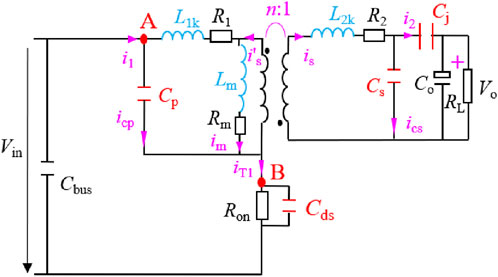
Figure 7. The equivalent circuit of flyback circuit at the turn on moment.
Based on Figure 7, the Equation 9 can be derived. When the duration td of the discontinuous stage is determined, the initial values of the voltage and current across the primary and secondary winding parasitic capacitors at the moment of turn-on satisfy Equation 10. By applying the Laplace transform to solve Equation 9, the time-domain equations for the port voltages (i.e., parasitic capacitor voltages) of the primary and secondary windings at the moment of turn-on can be obtained. Substituting these into Equation 11 allows further solution of other key waveforms in the flyback circuit at this moment.
At the turn-on moment, a peak in the primary current occurs, and the secondary side also experiences voltage and current oscillations. However, at this time, the oscillation frequencies of the primary and secondary sides are different. Their resonance frequencies are determined by their circuit parameters respectively and can be estimated using Equation 12, where frp represents the primary resonance frequency and frs represents the secondary resonance frequency.
3.4 The waveforms of flyback circuit at conduction interval
This article suggests that during the conduction period, the voltage of primary-side capacitor Vcp is clamped by the input voltage, and the magnetizing current can be considered to steadily increase under constant voltage excitation, while the secondary-side current is zero. Therefore, the equivalent circuit during the conduction period needs to consider the influence of the magnetizing loop, as shown in Figure 8. Based on this, the corresponding circuit Equation 13 can be derived, which can be simplified to Equation 14. In DCM mode, it can be assumed that the initial value of the primary current i1_on2 (0) is zero. However, when the oscillation time trn at the moment of turn-on is determined, Equation 15 can also be used to estimate i1_on2 (0).
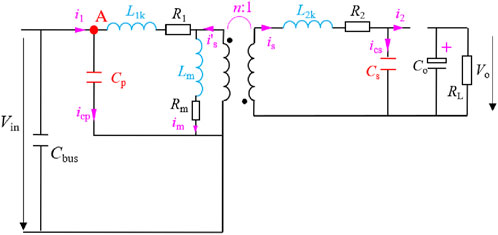
Figure 8. The equivalent circuit of flyback circuit at the conduction interval.
3.5 The waveforms of flyback circuit during full period
The previous sections have introduced the circuit equations and their solution methods for each switching process in the flyback circuit, which can be used to construct the main waveform characteristics of the circuit during each switching process. However, to fully draw the switch waveforms for the entire cycle, it is necessary to determine the duration of each switching process.
When analyzing the duration of each switching process, this article estimates using ideal primary and secondary current waveforms, as shown in Figure 9, ignoring the influence of winding resistances R1 and R2 on the switch waveforms. Although in the DCM mode of the flyback circuit, the circuit operation can be divided into four states: turn-off moment, discontinuous period, turn-on moment, and conduction period, considering that the waveform oscillation at the turn-on moment is relatively short, this article ignores its time proportion during analysis. Therefore, in Figure 9, only three time periods are shown: the conduction time ton, the diode freewheeling time toff, and the discontinuous time td.
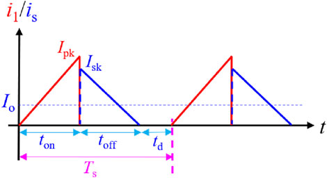
Figure 9. The input and output current waveforms with ideal assumption.
Given the output power Po and output voltage Vo, the average output current Io can be calculated using Equation 16. According to Figure 9, Io also satisfies Equation 17. During the period of toff, when ignoring the effect of R2, Equation 18 can be derived. During the period of ton, when ignoring the effect of R1, Equation 19 can be derived. The input peak current Ipk and the output peak current Isk satisfy the rule of ampere-turns balance, as shown in Equation 20. By combining Equations 16, 20, the conduction time ton and the output diode freewheeling time toff can be determined, as shown in Equation 21. The discontinuous time td is then equal to the switching cycle minus ton and toff, as shown in Equation 22.
Based on the above analysis and combining the time-domain equations for each stage, the required circuit waveforms for the entire cycle can be written. Taking the voltage of the primary-side MOSFET and the secondary-side diode as examples, their equations for the entire cycle can be represented by Equations 23, 24, respectively.
To specifically draw the switch waveforms, it is accepted to assume the following parameters: an output power Po of 28 W, an input voltage Vin of 380 V, an output voltage Vo of 12 V, a switching frequency fs of 65 kHz, primary and secondary winding turns ratio of 40:10, a load resistance Ro of 5.1Ω, a secondary-side diode forward voltage VD of 0.5 V, and relevant distributed parameters as shown in Table 1.

Table 1. The distributed parameters of flyback circuit.
According to the analysis in Section 3-1, the values of R1, R2, and Rm are affected by frequency. Based on the given parameters, the resonant frequency fr1 of the primary circuit at the turn-off moment can be calculated as 5.18 MHz. Accordingly, it is assumed that at this time, R1 = 30Ω, Rm = 2Ω, and R2 = 5Ω. During the discontinuous period, the primary resonant frequency fr2 is 741 kHz, and it is assumed that at this time, R1 = 10Ω, Rm = 1Ω, and R2 = 3Ω. At the turn-on moment, it is assumed that R1 = 30Ω, Rm = 30Ω, R2 = 5Ω, L1w = 10nH, and R1w = 5Ω. During the conduction period, it is assumed that R1 = 30Ω, Rm = 30Ω, and R2 = 1Ω.
Based on the given parameters and combining Equations 23, 24, the complete cycle waveforms of the switch transistor’s drain-source voltage and the secondary-side diode voltage can be plotted, as shown in Figure 10.
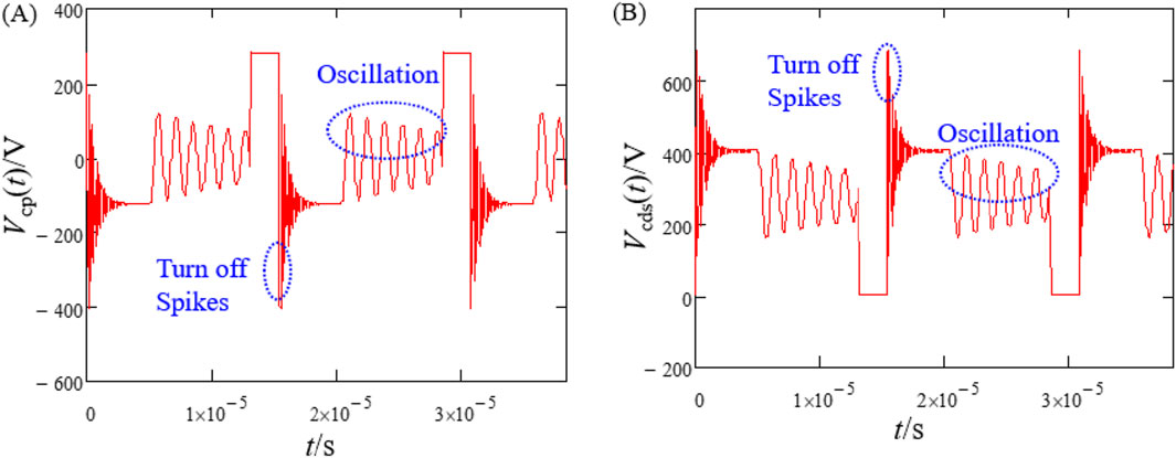
Figure 10. The complete cycle waveform of the primary-side MOSFET’s drain-source voltage and secondary-side diode voltage. (A) Voltage waveform of primary-side MOSFET’s drain-source. (B) Voltage waveform of secondary-side diode.
4 The distributed parameters influence on differential and common-mode noise
According to the analysis in Section 3, the distributed parameters of the flyback circuit have a significant impact on various voltage and current waveforms. The spikes and oscillations in these waveforms are also the fundamental causes of EMI noise generation. Therefore, performing Fourier decomposition on these voltage and current waveforms can reveal the distribution of the noise spectrum they generate.
According to the analysis in Section 3-1, the generation mechanism of differential-mode noise is mainly due to the current ripple in the primary power loop. Therefore, to analyze the impact of distributed parameters on differential-mode noise, Fast Fourier Transform (FFT) can be performed on the primary current i1. Common-mode noise is primarily caused by ground distribution currents arising from potential jumps in the circuit. Thus, to analyze the impact of distributed parameters on common-mode noise, FFT can be performed on the primary switch transistor voltage Vcds and the secondary diode voltage VD.
4.1 The distributed parameters influence on differential mode noise
Based on the analysis in Section 3, different primary current waveforms corresponding to various distributed parameters can be constructed and subjected to FFT decomposition to obtain the corresponding noise spectrum, as shown in Figure 11. It can be concluded that an increase in capacitance Cp, Cds, and primary leakage inductance L1k will worsen the differential-mode noise in the low-frequency range but improve it in the high-frequency range. It is observed that due to the smaller value of Cp, its impact is much less than that of Cds. Moreover, as Cp, Cds, and L1k increase, the frequency corresponding to the noise peaks in the mid-to-high frequency range of differential-mode noise decrease. This undoubtedly requires the filter to enhance its low-frequency filtering performance, increasing the difficulty of filter design. The distributed parameters L2k and Cs of the secondary circuit have essentially no effect on differential-mode noise.
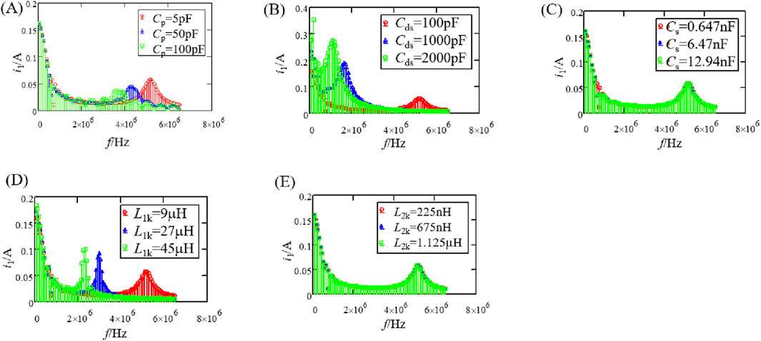
Figure 11. FFT results of the primary current i1 under different parasitic parameters. (A) Different values of Cp. (B) Different values of Cds. (C) Different values of Cs. (D) Different values of L1k. (E) Different values of L2k.
4.2 The distributed parameters influence on common mode noise
Similarly, by constructing the primary switch transistor voltage waveforms and secondary diode voltage waveforms corresponding to different distributed parameters, and performing FFT decomposition to obtain the corresponding common-mode noise spectrum, as shown in Figures 12, 13, the following conclusions can be drawn:
(1) Due to changes in the secondary winding leakage inductance L2k and parasitic capacitance Cs, the FFT results of Vcds and VD remain essentially unchanged. Therefore, the secondary circuit parameters have essentially no effect on common-mode noise.
(2) When the primary winding parasitic capacitance Cp and leakage inductance L1k increase, the frequency corresponding to the peaks of common-mode noise in the mid-to-high frequency range decrease, while the high-frequency common-mode noise is reduced. However, the impact on low-frequency common-mode noise is relatively minor.
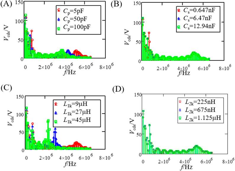
Figure 12. FFT results of the MOSFET voltage Vcds under different parasitic parameters. (A) Different values of Cp. (B) Different values of Cs. (C) Different values of L1k. (D) Different values of L2k.
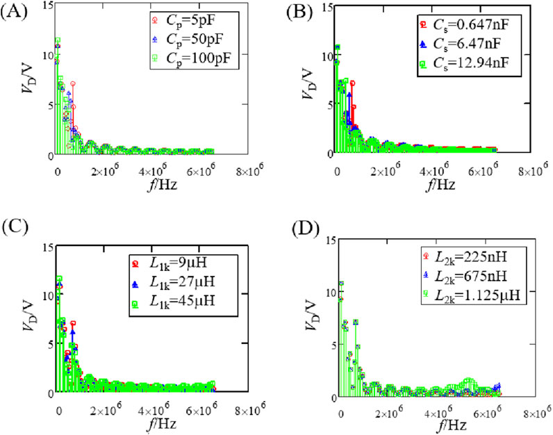
Figure 13. FFT results of the diode voltage VD under different parasitic parameters. (A) Different values of Cp. (B) Different values of Cs. (C) Different values of L1k. (D) Different values of L2k.
5 Experimental verification
The main purpose of this experiment is to verify two aspects, one is to confirm the accuracy of the theoretically constructed switching waveforms, and the other is to validate the effectiveness of analyzing the impact of distributed parameters on EMI noise based on these theoretically constructed switching waveforms. The flyback converter prototype used in this chapter is shown in Figure 14, and its circuit distributed parameter data as shown in Table 1.
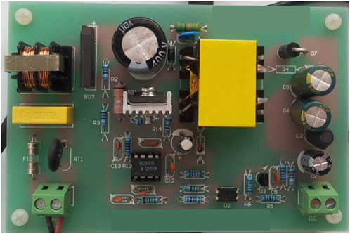
Figure 14. The prototype of flyback converter.
As shown in Figure 15, it includes comparison diagrams between the theoretically calculated main switching waveforms and the measured waveforms. It can be seen that the theoretically calculated switching waveforms accurately reflect the characteristics of each switching waveform during every switching process. There are some differences in peak amplitudes, mainly because there are errors between the values of circuit parameters used in the theoretical analysis and their actual values. However, this does not hinder the use of theoretical switching waveforms for analyzing the impact of flyback distributed parameters on its EMI noise. It should be noted that the time corresponding to each stage of these theoretically calculated waveforms is given based on the measured values, rather than calculated according to the formulas in Section 3–5. This is because Equations 21, 22 ignore the effect of winding resistance, and due to errors in the values of parameters such as leakage inductance and magnetizing inductance, it is impossible to achieve the same calculation results for each stage time as the measured values. To facilitate the comparison of theoretical switching waveforms and measured waveforms, this paper uses the actual measured values of each duration in the theoretical analysis.
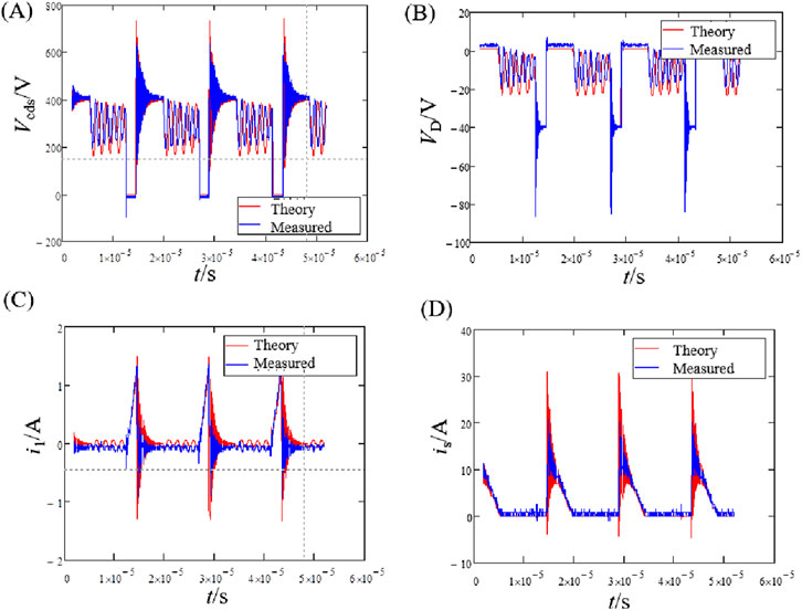
Figure 15. Comparisons of theoretical waveforms and measured waveforms. (A) Waveform of Vcds. (B) Waveform of VD. (C) Waveform of I1. (D) Waveform of Is.
To verify the correctness of using the constructed switching waveforms to analyze the impact of distributed parameters on EMI noise, this paper measured the differential and common-mode noise for different values of primary winding capacitance Cp and secondary winding capacitance Cs, as shown in Figure 16. It can be concluded that as Cp increases, its impact on low-frequency differential and common-mode noise is relatively minor, and the frequency corresponding to the peaks of differential and common-mode noise at mid-to-high frequency decrease. In contrast, changes in Cs have essentially no effect on the differential and common-mode noise of the entire converter. This conclusion is consistent with the results of theoretical analysis, further validating the effectiveness of the proposed theoretical method for time-domain analysis of the impact of flyback distributed parameters on EMI noise.
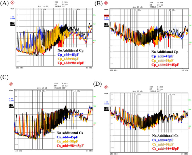
Figure 16. Experimental results of parasitic parameters’ effect on DM and CM noise. (A) The effect of Cp on CM noise. (B) The effect of Cp on DM noise. (C) The effect of Cs on CM noise. (D) The effect of Cs on DM noise.
6 Conclusion
This paper constructs theoretical time-domain waveforms for the flyback circuit considering transformer distributed parameters, analyzes the impact of transformer distributed parameters on voltage and current waveforms, as well as their effect on EMI noise. Experimental validation confirms the correctness and effectiveness of the established model. The following conclusions can be drawn:
(1) The constructed theoretical time-domain waveforms match the measured results, accurately expressing the details of the entire cycle’s voltage and current waveforms, such as the oscillation characteristics of each part.
(2) Analyzing the impact of flyback circuit distrib1uted parameters on differential and common-mode noise based on the constructed theoretical waveforms aligns with the trends of the measured noise results, which can guide the design of transformer distributed parameters and EMI rectification.
(3) The distributed parameters of the primary circuit in the flyback circuit have a larger impact on its EMI noise, while those of the secondary circuit have a smaller effect.
Data availability statement
The original contributions presented in the study are included in the article/supplementary material, further inquiries can be directed to the corresponding author.
Author contributions
BL: Writing–original draft. RL: Writing–review and editing. JJ: Writing–review and editing. YW: Writing–review and editing. PX: Writing–review and editing.
Funding
The author(s) declare that no financial support was received for the research, authorship, and/or publication of this article.
Conflict of interest
Authors BL, JJ, YW, and PX were employed by Ginlong Technologies Co., Ltd.
The remaining author declares that the research was conducted in the absence of any commercial or financial relationships that could be construed as a potential conflict of interest.
Generative AI statement
The author(s) declare that no Generative AI was used in the creation of this manuscript.
Publisher’s note
All claims expressed in this article are solely those of the authors and do not necessarily represent those of their affiliated organizations, or those of the publisher, the editors and the reviewers. Any product that may be evaluated in this article, or claim that may be made by its manufacturer, is not guaranteed or endorsed by the publisher.
References
Emami, Z., Farzanefard, H., and Motahari, S. R. (2010). “Precise prediction of conducted EMI in PWM flyback converters,” in 2010 18th Iranian conference on electrical engineering, 765–771.
Fakhafkh, L., and Ammous, A. (2017). New simplified model for predicting conducted EMI in DC/DC converters. Electr. Eng. 3, 1087–1097. doi:10.1007/s00202-016-0474-2
Fu, K. C. W. (2019). Evaluation method of flyback converter behaviors on common-mode noise. IEEE Access 7, 28019–28030. doi:10.1109/access.2019.2902462
Kai, T., Kashihara, T., and Kobayashi, K. (2024). “EMI noise analysis using frequency domain simulation considering dynamic semiconductor characteristics in flyback converter circuits,” in 2024 IEEE joint international symposium on electromagnetic compatibility, signal and power integrity: EMC Japan/asia-pacific international symposium on electromagnetic compatibility (EMC Japan/APEMC okinawa), 156–158.
Liang, B., Wei, K., and Yue, Y. (2012). Prediction of the conducted EMI in PWM converter system with parasitic parameters considered. Sci. China-Technological Sci. 10, 2829–2836. doi:10.1007/s11431-012-4925-3
Liu, J., Wang, Y., Jiang, D., and Cao, Q. (2015). “Fast prediction for conducted EMI in flyback converters,” in 2015 IEEE international conference on computational electromagnetics, 247–249.
Ma, W., Zhao, Z., Meng, J., Pan, Q., and Zhang, L. (2008). Precise methods for conducted EMI modeling, analysis, and prediction. Sci. China 6, 641–655. doi:10.1007/s11431-008-0082-0
Takahashi, K., Ibuchi, T., and Funaki, T. (2019). Frequency-domain EMI simulation of power electronic converter with voltage-source and current source noise models. IEICE Trans. Commun. 9, 1853–1861. doi:10.1587/transcom.2018ebp3301
Trinchero, R., Stievano, I. S., and Canavero, F. G. (2015). EMI prediction of switching converters. IEEE Trans. Electromagn. Compat. 5, 1270–1273. doi:10.1109/temc.2015.2419974
Wang, Z., Wang, S., Kong, P., and Lee, F. C. (2012). DM EMI noise prediction for constant on-time, critical mode power factor correction converters. IEEE Trans. Power Electron. 7, 3150–3157. doi:10.1109/tpel.2011.2182059
Yang, L., Wang, S., Zhao, H., and Zhi, Y. (2020). Prediction and analysis of EMI spectrum based on the operating principle of EMC spectrum analyzers. IEEE Trans. Power Electron. 1, 263–275. doi:10.1109/tpel.2019.2914468
Keywords: time domain, distributed parameters, flyback, EMI, equivalent circuit
Citation: Liu B, Li R, Ji J, Wang Y and Xu P (2025) Time domain analysis of flyback EMI based on distributed parameters theory. Front. Electron. 6:1538379. doi: 10.3389/felec.2025.1538379
Received: 02 December 2024; Accepted: 17 January 2025;
Published: 13 February 2025.
Edited by:
Wenping Zhang, Tianjin University, ChinaReviewed by:
Lin Subin, Fuzhou University, ChinaQingbin Chen, Fuzhou University, China
Kaining Fu, Xiamen University of Technology, China
Copyright © 2025 Liu, Li, Ji, Wang and Xu. This is an open-access article distributed under the terms of the Creative Commons Attribution License (CC BY). The use, distribution or reproduction in other forums is permitted, provided the original author(s) and the copyright owner(s) are credited and that the original publication in this journal is cited, in accordance with accepted academic practice. No use, distribution or reproduction is permitted which does not comply with these terms.
*Correspondence: Rui Li, liruiqd@sjtu.edu.cn