 Wenkuan (Kevin) Man
 Thomas Bifano*
- Boston University Photonics Center, Boston University, Boston, MA, United States
Introduction: This work presents a prototype electromagnetic actuation deformable mirror (DM) assembly with stress-resilient face sheet design.
Methods: The DM face sheet design includes slender micromachined silicon pillars that are integrated with a silicon face sheet to reduce unpowered face sheet surface distortion caused by actuator adhesion stress.
Results: The assembled deformable mirror prototype allowed bi-directional actuation with total stroke exceeding 20 μm. A two-step control method was used to improve the prototype dynamic performance, allowing settling time on the order of 1 ms. Prescribed references shapes were made on the prototype deformable mirror using closed-loop control.
Discussion: While the simplified DM produced in this work has only 19 actuators and therefore has limited capacity to control complex shapes, the design and fabrication processes described and demonstrated in this work provide a promising approach to development of high-stroke magnetic DMs.
1 Introduction
Deformable mirrors (DMs) are devices that can correct wavefront aberrations and achieve wavefront control through active control. DMs are most often used in adaptive optics (AO) systems, in which many actuators in parallel are used to distort the mirror surface in direct response to a measured wavefront distortion or in indirect response to a measure of image quality. AO is now widely used in ground-based large-aperture telescope imaging to compensate effects of atmospheric turbulence. DMs have also been applied in other fields, including microscopy (Booth, 2007; Sherman et al., 2002; Ziph-Schatzberg et al., 2009), communication (Ziph-Schatzberg et al., 2009; Li et al., 2014), vision science (Horsley et al., 2005; Chen et al., 2007), laser beam shaping (Anscombe, 2010; Schroeder et al., 2010; Tran et al., 2014; Jochmann et al., 2013) and pulse shaping (Hasegawa and Hayasaki, 2021).
Metrics of performance of DMs include actuator stroke, actuator number, actuation response time, mirror diameter, and mirror surface quality, among others. DM actuation has been demonstrated using a wide range of modalities, including thermal, mechanical, electrostatic, piezoelectric, and magnetic actuators. Guided by application-specific constraints, DMs have been produced with apertures ranging from meter scale to millimeter scale.
In many DM architectures, arrays of actuators are adhesively bonded to a nominally planar, reflective face sheet. Surface-normal exertion of the actuators locally deforms the face sheet. A DM design parameter is the mechanical stiffness of the face sheet, which needs to be large enough to avoid unwanted deformation of the face sheet due to residual stresses resulting from adhesive assembly, but small enough to allow adequate actuator stroke, given the maximum achievable surface-normal force that the actuator can apply to the face sheet. In the past, a common manufacturing and assembly approach for this type of DM has been to use low stress adhesives to bond actuators to the face sheet, and to design the face sheet to be stiff enough to so that its flatness error would be below some threshold value after actuator adhesion.
In this work, we describe a protype DM made using a previously reported design innovation that relaxes this design constraint by moving the adhesion surfaces to the distal ends of an array of slender posts attached to the face sheet, thereby substantially reducing the effect of residual adhesive stresses on face sheet deformation. This allowed us to use a thin, compliant face sheet, allowing large stroke. The prototype DM uses permanent magnets adhesively bonded to the distal ends of the slender posts and a fixed array of independently addressable electromagnetic, current-driven actuation coils to shape the face sheet surface.
Electromagnetically actuated DMs have been reported previously. Appealing aspects of this type of DM, from a manufacturing standpoint, is that the actuation uses low voltage and can be achieved with low-cost electronic drivers; drive coils are easily fabricated from wound conductors; and permanent magnets that are displaced by applied magnetic fields can be purchased at low cost. Among the earliest prototype demonstrations of such DMs was a device made by Divoux et al. (1998). Many alternative approaches and geometries of including large-format DMs for astronomical applications (Hamelinck, 2010), space-based adaptive optics, (Doelman et al., 2017), and adaptive optics for imaging (Cugat et al., 2001). Performance tradeoffs with respect to DM design characteristics have been detailed elsewhere (Madec, 2012). A differentiating aspect of the current work is the use of MEMS fabrication with deep reactive ion etching to create a monolithic single-crystal silicon mirror face sheet with integral posts. That approach substantially reduces the impact of adhesion-induced stresses in assembly (Man and Bifano, 2023). In addition, the MEMS fabrication approach allows smaller inter-actuator spacing, or pitch, allowing more compact DM formats. Finally, the prototype DM described in this work allows a unique combination of high actuator stroke (∼20 µm), small actuator pitch (∼1.5 mm), and high actuator speed (>500 Hz settling time).
The number of actuators required in a deformable mirror for a given application is determined by the spatial frequency of aberrations to be compensated. In the simplest applications requiring only control of focus or astigmatism, DMs with tens of actuators can be sufficient (Jiang et al., 1991). In astronomical imaging and coronagraphic applications, DMs with thousands of actuators are often required. For the purposes of this prototype demonstration, a hexagonal distribution of only 19 actuators was chosen, to simplify fabrication and experimentation.
A cross-sectional schematic of the prototype concept is depicted in Figure 1.
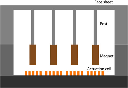
Figure 1. Cross sectional schematic of the prototype DM structure actuated by a coil array.
2 The design (face sheet and actuation system)
The face sheet was designed to be comprised of a thin (10 µm) single crystal circular element supported by an integrated array of single crystal silicon posts, each measuring 500 µm long and 300 µm in diameter, and distributed laterally in a hexagonal array with 1.5 mm spacing. These two subsystems (face sheet and post array) were fabricated out of silicon on insulator (SOI) polished wafer with a 10 µm thick device layer and 500 µm thick handle layer, connected by a 0.5 µm thick thermally grown silicon dioxide layer. Etching of the handle layer to define posts and face sheet frame was achieved through deep reactive ion etching (DRIE). The fabricated face sheet has circular mirror aperture with diameter of 12 mm. Nineteen posts were distributed in the hexagonal array.
A photograph and two SEM micrographs of the fabricated face sheet with integral posts are depicted in Figure 2, for a test device made with 37 posts measuring in a hexagonal layout with 1.5 mm post spacing. This mirror face sheet measures 12 mm in diameter and is 10 µm thick and was fabricated using deep reactive ion etching (DRIE) of a polished silicon on insulator (SOI) wafer having a 500 µm thick handle layer and a 10 µm thick device layer. A photoresist lithography mask was used to define the etching geometry. DRIE processing parameters were optimized to reduce the cross sections of the posts near their attachments to the mirror. The eight peripheral through holes in the SOI wafer were used for alignment of the face sheet with separately fabricated silicon template with eight alignment pins and nineteen cylindrical cavities. Magnets were manually deposited into the cavities in the template, and each was topped with a small drop of adhesive. The face sheet and the template were manually assembled, forcing each magnet to contact a corresponding post. The adhesive was cured using UV illumination, and the template was removed, leaving the magnets permanently affixed to the post ends. This assembly was then aligned with a fixed array of electromagnetic coils, with a predefined gap between the free ends of the magnets and the tops of the coils. The gap was fixed using precision shims and precision spring loading of the face sheet and coil assemblies.
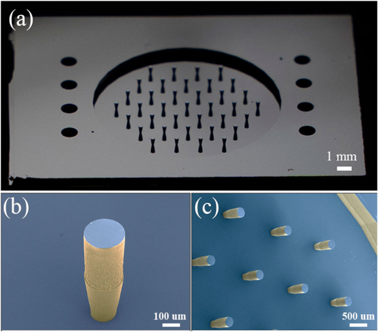
Figure 2. Images of the fabricated face sheet with integral posts. (A) Photo of fabricated face sheet integrated with posts; (B) SEM image of a single post and (C) SEM image of fabricated posts on the face sheet.
An electromagnetic model developed in MATLAB was used to simulate the electromagnetic field of the prototype DM.
The electromagnetic field simulation was based the Biot-Savart Law for a single coil turn:
Where H(z) is induced magnetic field along the central axis of the coil, I current in the coil, r is the radius of the coil, z is the elevation above the coil central axis. For a multiple turn coil, the total magnetic field is the sum of magnetic field of each loop, using the corresponding radius and elevation of that loop. If a cylindrical magnet is placed above the coil, with cross-sectional area A and height h, the force exerted on the magnet by the coil is the integral of the magnetic field gradient along the z-axis, with integral limits corresponding to the z coordinates spanned by the magnet:
Where Fz is the total force exerted on the magnet, and Br is the remanence of the magnet. Equation 1 and Equation 2, along with well-known mathematical models for mechanical stiffness of an elastic plate in response to a surface-normal actuator force (Young, 1989) can be used to develop designs for an electromagnetic DM, given constraints and performance objectives for the design. Constraints include power (e.g., the maximum power that can be effectively dissipated through resistive heating when driving each actuator), geometry (e.g., coils need to conform to actuator pitch limitations), and materials (e.g., permanent magnet remanence for commercially available magnets is limited). Objectives include stroke (e.g., ± 10 µm was desired for the prototype, influencing minimum gap selection) and resonant frequency (e.g., >500 Hz). A MATLAB numerical model combining these factors was developed, and the effects of changing coil geometries (e.g., number of turns in the coil, coil wire diameter, and number of coil layers), actuator gap, magnet geometry, and applied current were simulated to determine the corresponding actuator performance.
In this model, cylindrical permanent magnets were simulated based on the characteristics of the actual magnets used in the prototype: 300 µm in diameter and 500 µm tall, with magnetic remanence of 1.4 T. The simulated electromagnetic field corresponded to the field generated by the actual coils: with inner and outside diameters of 200 µm and 1,100 μm, respectively.
Through this simulation, a prototype electromagnetic coil geometry was selected, comprised of a multiple turn spiral coil with 6 turns in plane and a total of four planes stacked atop one another along the z-axis. The designed coil has 200 µm inner diameter and 1,100 µm outer diameter and was made from copper wire with 75 µm diameter. The properties of commercially available magnets were used in the simulation: each magnet measured 300 µm in diameter and 500 µm tall, with magnetic remanence of 1.4 T. The simulation included parametric optimization of applied force for a given input current, which is dependent on gap, coil geometry, and magnet properties. The simulated value of force as a function of gap for this geometry is shown in Figure 3.
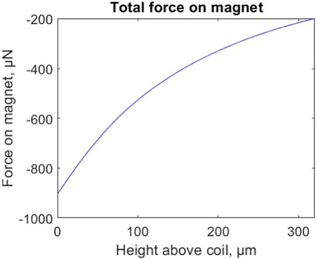
Figure 3. Simulated force on magnet from induced magnetic field as a function of gap between the top of the coil and the bottom of the magnet, with coil input current of 0.5A, coil diameter of 1,100 μm, comprised of a six-turn spiral four layers deep. Based on mechanical simulations of the edge-supported face sheet, a central actuator exerting a force of 800 µN would be sufficient to achieve 10 µm deflection.
An additional design parameter is the geometry of the integral posts depicted in Figure 2. This geometry does not affect actuation force or stroke but has an impact on mirror face sheet stresses due to adhesion to magnets (Man and Bifano, 2023). Long, slender posts help to reduce the deformation of the mirror face sheet due to those stresses.
3 DM protype assembly
Miniature custom copper wire coils were fabricated for this project (Audemars Microtec, Cadempino, Switzerland). Coils were wound from 75 µm diameter copper wire with 2 µm thick insulating polyimide sheathing to form a multi turn inductor with 6 turns in plane and 4 spiral layers along the coil center axis. Each coil has two 7 mm long leads. The body of the coil has an inside diameter of 200 µm and outside diameter of 1,100 µm. Photographs of a fabricated multi turn copper coil are shown in Figure 4. The measured dimensions and electrical resistance of the coil is shown in Table 1.
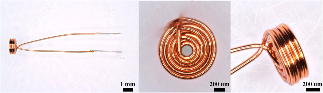
Figure 4. Photos of customized multi turn copper solenoid from different perspectives.

Table 1. Mean values of dimensions and resistance for multi turn solenoids.
Sample coils were power tested by applying current to them and ramping that current slowly from 100 mA to the point of failure, which occurred due to heat-induced breakdown of the wire insulation. This occurred at a current of 750 mA, corresponding to an approximate power of 225 mW (for a coil with 0.3 Ω resistance).
A coil array mounting device was fabricated in aluminum and assembled on an aluminum base to form actuation system. This mounting device allows independent electrical connections to both leads of each coil to allow current control through a custom-made printed circuit board (PCB). Nineteen coils were placed into the mounting device, orienting the coils in a hexagonal arrangement that matches the face sheet integral post array, with 1.5 mm spacing. The assembled actuation system with 19 actuators is shown in Figure 5.
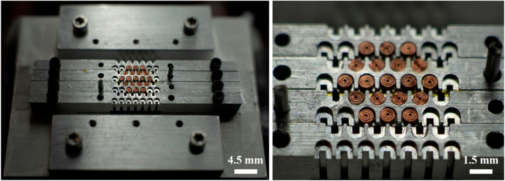
Figure 5. Photo of assembled actuation subsystem. 19 coils are positioned into coil mounting plates that are attached to a base plate. Two aluminum shim plates (at the top and bottom of the left image) provide reference mounting planes for the DM face sheet structure.
Nineteen cylindrical permanent neodymium magnets were attached through adhesive bonding to the free ends of the face sheet posts through parallel assembly using a precision fabricated alignment template and an external electromagnet to hold the permanent magnets in place as the adhesive cured. Precision alignment holes in the face sheet assembly and the actuator coil assembly allowed pin alignment of the actuator array with attached permanent magnets to the coil actuator array. A spring-loaded aluminum top plate and spacer shims were used to control the gap between the face sheet assembly with attached permanent magnets and the coil actuator array.
4 Characterization and measurement
The fabricated face sheet surface profiles were measured using a surface mapping interferometer (Zygo NewView™ 9000, Zygo Corporation) before assembly, both with and without magnets attached. A custom-built partitioned aperture wavefront (PAW) surface measuring device (Barankov and Mertz, 2013) was employed to measure face sheet surface topography during static actuation tests and shape control tests. A commercial multiple channel voltage driver system from Boston Micromachines Corporation was used to interface with the control computer, and a custom-designed 19 channel voltage-to-current conversion circuit was designed, built and used to provide actuation power to the 19 independent actuator coils. Local dynamic response of the assembled DM face sheet was measured and recorded using a capacitive displacement gauge (ADE, MicroSense 3401). Advanced drive control (two step control, described in the next section) was achieved using a digital delay generator (DG646, Stanford Research System) and amplifier modules (SIM 954, SIM 983 and SIM980, Stanford Research System).
5 Results and discussion
A cross-sectional schematic of the process used to manufacture the face sheet with integral posts is illustrated in Figure 6A. The process begins with a double-side polished SOI wafer comprised of a 10 µm thick single crystal silicon device layer, a 0.5 µm thick thermally grown silicon dioxide layer, and a 500 µm thick single crystal silicon handle layer. The handle layer is patterned lithographically with photoresist that serves as a mask for the DRIE etching process. The handle layer is etched using DRIE, and etching is stopped by the buried oxide layer. This, etch defines the post array, the face sheet edge-supporting frame, and the through-holes for subsequent device alignment and assembly. Next, the exposed oxide layer is removed, to eliminate stress that it might exert on the face sheet. Finally, the device layer is patterned to complete etching of the alignment holes.
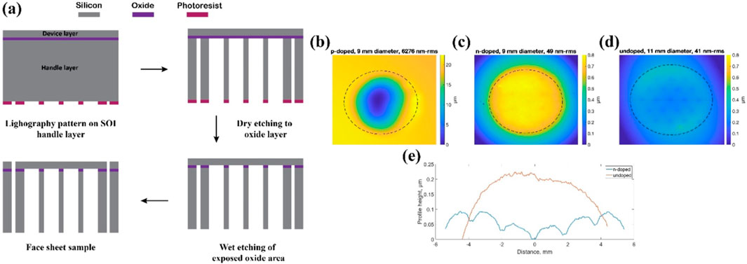
Figure 6. (A) Schematic of face sheet fabrication process; (B–D) Measured surface profile of face sheets with differently doped device layers; and (E) Comparison of surface profiles through the main diameter of the n-doped and undoped surface maps.
SOI wafers can be doped with phosphorous (n-type) or boron (p-type) to alter electrical conductivity of the device layer, as is needed in some electronics applications. One result of such doping is the creation of residual stresses in the device layer. We found that these residual stresses could be substantial, deforming the face sheet after DRIE etching to form the face sheet and post array. DRIE-etched SOI wafers with device layers having different doping conditions (n-type doped, p-type doped and undoped) were used to demonstrate this effect on the face sheet assembly (Figures 6B–E). After etching, the three face sheets were measured using a surface mapping interferometer. The p-type doped face sheet had a concave surface with a peak deformation of 20 μm, and a flatness error over the face sheet aperture of more than 6 µm-rms. The n-type doped face sheet had a convex surface with a peak deformation of 800 nm, and a flatness error over the face sheet aperture of 49 nm-rms. The undoped device layer had a nominally flat surface, with peak deflection of 300 nm and a flatness error over the face sheet aperture of 41 nm-rms. The result demonstrates that it is important to use SOI wafers with undoped device layers to achieve a flat face sheet after DRIE etching.
A face sheet with a 12 mm diameter active aperture and 19 integral posts was fabricated, and cylindrical magnets were adhesively attached to the posts as described previously. All magnets were oriented with the same magnetic polarity. Magnetic repulsion among the magnets resulted in a net outward force at the magnet layer, which was then translated through the posts to exert a bending moment on the face sheet. This moment loading on the face sheet at the periphery of the actuator array caused a large, circumferentially symmetric, downward deflection of the face sheet inside the actuator array (spanning 9 mm) and a smaller, circumferentially symmetric downward deflection of the face sheet outside of the actuator array (between the 9 mm actuator edge and the 12 mm face sheet aperture. The resulting face sheet deformation is shown in the surface map of Figure 7B and in the cross section of Figure 6D. The face sheet peak deformation was ∼3 μm, leading to a flatness error over the face sheet aperture of 828 nm-rms. This error is substantial, though potentially correctable using the actuators.
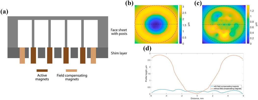
Figure 7. (A) Cross-sectional schematic of post-mounted actuator magnets and rigid field compensating magnets; (B) Measured topography of a face sheet with 19 actuator magnets alone, illustrating substantial face sheet deformation due to actuator magnet in-plane repulsion that generates bending moments in the face sheet; (C) Measured topography of the same face sheet with magnetic repulsion compensated through the addition of a ring of rigidly mounted field-compensating magnets; and (D) Comparison of surface profiles across the main diameter of the two surface maps.
A design modification was developed to counteract this magnetic repulsion. A peripheral ring of identical “field compensating” magnets were embedded rigidly in a shim layer, surrounding actuator magnets. A cross-sectional schematic of this approach is shown in Figure 7A. These field-compensating magnets exert a counterbalancing magnetic field, substantially reducing the net moment that is transferred from the actuator magnets to the face sheet.
In the final prototype design, nineteen field-compensating cylinder magnets were adhesively mounted in a shim structure and distributed evenly around the post array. The peak-to-valley face sheet surface flatness was measured to be less than 635 nm after this design modification within the circular area defining the mirror, with a flatness error over the that same area of 127 nm-rms as shown in Figure 7C and in the cross section of Figure 7D. It was found that this nominal unpowered surface flatness could be reduced to 85 nm-rms through subsequent application of closed-loop control.
With actuator magnets and field-compensating attached, the face sheet assembly and shim plate were aligned with the coil assembly The shim, comprised of alignment holes and field-compensating magnets, was designed with precise thickness to control the gap between the tops of the coils and the bottoms of the magnets. This gap was nominally set to be 20 µm. A spring-loaded clamp compressed the three layers (face sheet and frame, shim, and coil assembly) with uniform pressure, leaving the clear aperture of the face sheet free from obstruction. A photograph of the assembled prototype DM is shown in Figure 8.
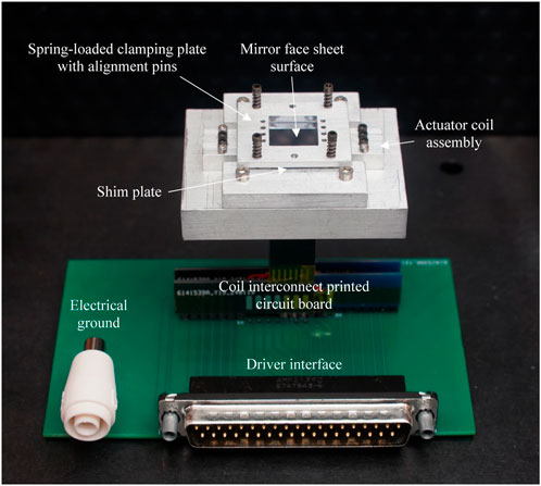
Figure 8. Photo of assembled DM prototype device with 3D actuator coils.
The final component of the prototype DM system is the current driver required for actuation of the inductive coils. A commercial 140-channel actuation system (Boston Micromachines Corporation MultiDM Driver) was adapted for this purpose. The architecture of the Boston Micromachines Corporation driver includes a PCB backplane comprised of a high-speed (10 kHz), low voltage (0–5 V) digital to analog (D/A) voltage converter array with a USB interface. For the prototype driver, custom-designed PCBs and an auxiliary power supply were integrated with the MultiDM driver backplane. The hybrid driver was capable of driving up to 19 channels at high current (0.7 A/channel) and high speed (10 kHz). The output of this driver was connected to the coil array using a custom-designed PCB that was integrated with the coil array assembly.
The surface topography of the face sheet of the assembled prototype DM was measured using a custom-built PAW photometric optical measuring device in response to actuation commands. A design goal was to achieve bidirectional peak deflection of at least ± 10 µm when energizing only the central actuator coil. Using the previously described current driver, a quasistatic current input was applied to the central actuator coil in the array. Negative peak displacement (actuator coil repelling magnet) reached −10 µm when the coil was energized with +0.63 A, with a surface map corresponding to that condition shown in Figure 9A. Positive peak displacement (actuator coil attracting magnet) reached +11 µm when the coil was energized with −0.58 A, with a surface map corresponding to that condition shown in Figure 9B. Surface deformation measurements were made for twenty different drive current conditions, ranging from −0.58 A to +0.63 A. At each condition, the peak actuation deflection was recorded. The results are shown in Figure 9C. Peak actuation displacement varies monotonically and nearly linearly with input current. For the same actuation displacement, higher current is required to repel the magnet than to attract it. This is consistent with the physical interpretation that electromagnetic field strength weakens slightly as the magnet-coil gap increases, as predicted by Equation 2.
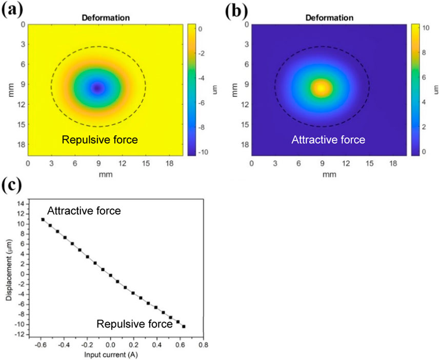
Figure 9. Static actuation tests of assembled DM with 19 magnets attached. (A) Negative peak displacement; (B) Positive peak displacement; (C) Peak displacement as function of different input currents; The black dashed circles in (A, B) outline the face sheet areas.
The data shown in Figure 9C correspond to the measured displacement of the mirror at a location above the central actuator in the DM when that actuator is energized. Displacements of the mirror measured at a location above any other actuator in the DM when that actuator is energized will be lower, for a given input drive current. While the exerted electromagnetic force is the same for all actuators subjected to a given input drive current, the mirror surface-normal stiffness is lowest at its center and increases toward its edges. From a simplified elastic analysis (Table 11.2.19 in reference (Young, 1989)), it is expected that the mirror displacement above an energized outermost actuator, which is located halfway between the mirror center and edge, will be 56% of that of the mirror displacement above the energized central actuator, given the same input current. This difference can be considered when using the mirror in a control system to compensate wavefront errors.
Interactuator stroke was also measured for this assembled DM, by actuating two adjacent actuators in opposite directions. In this case, the relevant measurable parameter is the maximum peak-to-valley difference between the face sheet deflections at the locations of those two actuators. In adaptive optics control, this parameter (interactuator stroke) is important because it determines the achievable amplitude at the highest spatial frequencies that the DM can correct. The measured interactuator stroke is shown in Figure 10, for current of +0.28 A applied to one actuator and −0.33 A applied to a neighboring actuator, with all other actuators unenergized. The interactuator stroke, defined as the difference between the highest and lowest points on the face sheet is 4.5 µm.
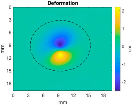
Figure 10. Interactuator stroke measurement. Two adjacent actuators in the prototype DM were energized in opposite directions with moderate current input (about half the maximum allowable current). The resulting net surface deformation of the mirror was found to have a peak-to-valley difference of 4.5 µm. This test is used in DM characterization to evaluate the achievable interactuator stroke.
The DM prototype’s dynamic actuation response was also measured. A 0.5 Hz square wave current input from 0.00 A to 0.26 A (corresponding to a displacement from 0.0 µm to 4.8 µm) was applied to the central actuator coil. Displacement of the face sheet directly over the actuator location was measured with a capacitance gage displacement sensor, averaging over a circular area of approximately 10 mm2. The measured actuator current and face sheet displacement were recorded, with results depicted in Figure 11. The dynamic step response of a MEMS mirror comprised of a fixed-edge elastic plate perturbed by a surface-normal point actuator can be approximated as a second order damped oscillation (Timoshenko and Woinowsky-Krieger, 1959). The theoretical natural frequency of such a resonator was derived analytically by Young (1989). The oscillation resonant frequency was 590 Hz and the damping ratio was 0.0059.
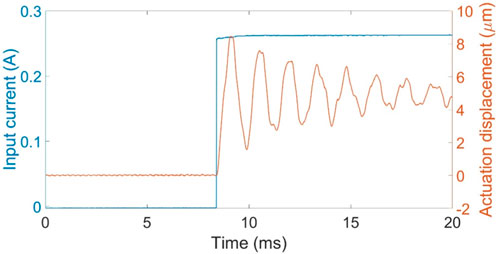
Figure 11. Dynamic displacement of the face sheet in response to a step change in input current. Blue data is input current, and the orange data is actuation displacement response.
For underdamped second order MEMS oscillators, advanced drive techniques have been developed to increase settling time. These techniques rely on changing the actuator input signal from that of a single step to one with two smaller steps separated by a precise delay, exploiting superposition of the linear elastic plate responses to the two steps to effectively cancel the oscillatory part of the mirror’s dynamic response (Imboden et al., 2016). A two-step open loop control approach was used to demonstrate a way to reduce face sheet oscillation and decrease settling time. In two-step control, an input step change corresponding to a fraction of the single-step input is applied to the second order system, which then begins its oscillatory response. At a time corresponding to ½ of the oscillation period, the remaining fraction of the single step input is added to the control signal. For the prototype DM, the first step was 52% of the total (0 A–0.135 A), while the second step was the remaining 48% of the total (0.135 A–0.260 A), applied 0.85 ms after the first step. The result of this two-step open-loop input control was to eliminate much of the oscillation in face-sheet displacement, though some more complex, lower amplitude oscillations remain evident in the measured response as shown in Figure 12.
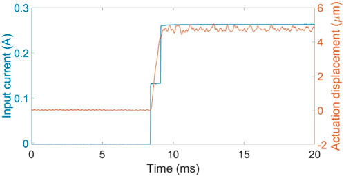
Figure 12. Dynamic actuation in a 19-actuator device with the center actuator driven using two-step control. Blue data is input current, and the orange data is actuation displacement response.
Closed loop control was conducted to achieve three prescribed shapes, tilt, astigmatism and defocus with the 19 actuator DM prototype.
In the closed loop control, the surface shape measured by the PAW sensor was used as the control feedback signal. The control algorithm proceeded as follows
1) Determine the location of an actuator’s peak influence on the face sheet by energizing that actuator with a nominal positive current input while all other actuators remained unenergized. Measure the resulting topography of the face sheet. Use an image analysis algorithm to locate the (x,y) position of the peak deflection. Repeat for all 19 actuators, establishing an array of 19 (x,y) control locations.
2) Provide the controller with desired reference displacement of the mirror ri at each of the control locations, where i is the coordinate index (19 in all).
3) Energize all actuators with an initial control input current uni, where n is the iteration number (initial value = 1), and i is the coordinate index. For simplicity, start with uni = 0.
4) Measure the mirror surface shape. Determine the current displacement dni at each control location, where n is the iteration number (integral values >1), and i is the coordinate index.
5) Establish the displacement error eni at each control location: eni= dni- ri.
6) Update the control input current un+1i= uni–g(eni) to all actuators, where g is an experimentally determined integral gain constant.
7) Repeat steps 4-6, incrementing n each time.
The control loop was iterated until steady state was reached. The number of iterations required to reach steady state depends strongly on the integral gain used in the control loop. Typically, steady state was reached in ten iterations. This control loop was implemented quasistatically, with each iteration taking ∼5 s. Nearly all of that time was associated with surface measurement.
Reference shapes and achieved shapes are shown in Figure 11 for three different shapes, and two polarities of each. For a 1.5 µm peak-to-valley tilt reference shape, the measured surface profile showed final surface error (the difference between reference shape and achieved shape) of about ∼40 nm-rms within the controlled region for both polarities, as shown in Figures 13A, B. For a 1.0 µm peak-to-valley astigmatism reference shape, the measured surface profile showed final surface error (the difference between reference shape and achieved shape) of about ∼35 nm-rms within the controlled region for both polarities, as shown in Figures 13C, D. For defocus reference shapes, the maximum achievable concave shape (attractive actuation) had a peak-to-valley range of 22 µm and the maximum achievable convex shape (repulsive actuation) had a peak-to-valley range of 17 μm, as shown in Figures 13E, F. In both cases, the final surface error (the difference between reference shape and achieved shape) was about ∼330 nm-rms. This larger shape error is attributed to the large range of displacements associated with this relatively extreme amplitude reference shape, along with the relatively small number of actuators in the prototype array.
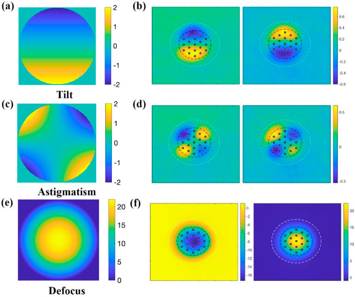
Figure 13. DM shape control through closed-loop control. Reference shape of tilt, astigmatism and defocus (A, C, E) and corresponding achieved shapes by DM (B, D, F). Face sheet edges are denoted by the white dotted lines in the surface maps, while active control regions for the reference shapes are denoted by black dotted lines. All scale bars in µm.
6 Conclusion
In this work, an electromagnetically actuated continuous surface deformable mirror has been designed, fabricated, and tested. The 19-actuator DM prototype made using 3D coils actuators was successful in many aspects of performance. A repeatable process for prototype fabrication was developed and demonstrated. With the prototype, individual actuator stroke was shown to be >10 µm in both directions, and collective actuator stroke was shown to have a range of 37 µm in positive and negative focus shape control experiments. Interactuator stroke exceeded 4 µm. A technique to flatten the DM prototype using compensating magnets and active control yielded prototype face sheet flatness of 85 nm-rms.
There were other areas in which the prototype did not meet performance targets. Its fundamental resonant frequency was about 580 Hz, somewhat less than the targeted 1 kHz. The most straightforward way to increase the resonant frequency would be to stiffen the face sheet by making it thicker, though that would also reduce achievable stroke.
Another area in which the prototype DM performance was less than ideal was in its dynamic behavior. Underdamping of the structure led to oscillation in response to step changes in actuator input current that took up to tens of milliseconds to decay to steady state. Advanced control techniques could be used to avoid underdamped oscillations, and the simplest of these, two-step control, proved effective in reducing the problem to some extent.
Data availability statement
The raw data supporting the conclusions of this article will be made available by the authors, without undue reservation.
Author contributions
WM: Conceptualization, Data curation, Formal Analysis, Funding acquisition, Investigation, Methodology, Project administration, Resources, Software, Supervision, Validation, Visualization, Writing–original draft, Writing–review and editing. TB: Conceptualization, Data curation, Formal Analysis, Funding acquisition, Investigation, Methodology, Project administration, Resources, Software, Supervision, Validation, Visualization, Writing–original draft, Writing–review and editing.
Funding
The author(s) declare that financial support was received for the research, authorship, and/or publication of this article. Office of Naval Research Grant N00014-17-1-2438 Boston Micromachines Corporation, Agmt dtd 4/28/2023.
Conflict of interest
TB acknowledges a financial interest in Boston Micromachines Corporation, which produces commercially available DMs.
The remaining authors declare that the research was conducted in the absence of any commercial or financial relationships that could be construed as a potential conflict of interest.
Generative AI statement
The author(s) declare that no Generative AI was used in the creation of this manuscript.
Publisher’s note
All claims expressed in this article are solely those of the authors and do not necessarily represent those of their affiliated organizations, or those of the publisher, the editors and the reviewers. Any product that may be evaluated in this article, or claim that may be made by its manufacturer, is not guaranteed or endorsed by the publisher.
References
Anscombe, N. (2010). Direct laser writing. Nat. Photonics 4 (1), 22–23. doi:10.1038/nphoton.2009.250
Barankov, R., and Mertz, J. (2013). Single-exposure surface profilometry using partitioned aperture wavefront imaging. Opt. Lett. 38 (19), 3961–3964. doi:10.1364/OL.38.003961
Booth, M. J. (2007). Adaptive optics in microscopy. Philosophical Trans. R. Soc. A Math. Phys. Eng. Sci. 365 (1861), 2829–2843. doi:10.1098/rsta.2007.0013
Chen, D. C., Jones, S. M., Silva, D. A., and Olivier, S. S. (2007). High-resolution adaptive optics scanning laser ophthalmoscope with dual deformable mirrors. J. Opt. Soc. Am. A 24 (5), 1305–1312. doi:10.1364/josaa.24.001305
Cugat, O., Basrour, S., Divoux, C., Mounaix, P., and Reyne, G. (2001). Deformable magnetic mirror for adaptive optics: technological aspects. Sensors Actuators A Phys. 89 (1), 1–9. doi:10.1016/S0924-4247(00)00550-1
Divoux, C., Cugat, O., Reyne, G., Boussey-Said, J., and Basrour, S. (1998). Deformable mirror using magnetic membranes: application to adaptive optics in astrophysics. IEEE Trans. Magnetics 34 (5), 3564–3567. doi:10.1109/20.717841
Doelman, N., Overtoom, T., Kuiper, S., Nieuwkoop, E., Russchenberg, T., van Riel, M., et al. (2017). “Electromagnetic deformable mirror for space applications,” in International conference on space optics — ICSO 2016, 10562. SPIE, 170. doi:10.1117/12.2296161
Hamelinck, R. F. M. M. (2010). Adaptive deformable mirror: based on electromagnetic actuators. Eindhoven, NL: Technische Universiteit Eindhoven. PhD Dissertation.
Hasegawa, S., and Hayasaki, Y. (2021). Femtosecond laser processing with adaptive optics based on convolutional neural network. Opt. Lasers Eng. 141, 106563. doi:10.1016/j.optlaseng.2021.106563
Horsley, D. A., Park, H., Laut, S. P., and Werner, J. S. (2005). “Characterization for vision science applications of a bimorph deformable mirror using phase-shifting interferometry,” in Ophthalmic Technol. XV, 5688, 26. doi:10.1117/12.591848
Imboden, M., Chang, J., Pollock, C., Lowell, E., Akbulut, M., Morrison, J., et al. (2016). High-speed control of electromechanical transduction: advanced drive techniques for optimized step-and-settle response of MEMS micromirrors. IEEE Control Syst. Mag. 36 (5), 48–76. doi:10.1109/MCS.2016.2584338
Jiang, W., Ling, N., Rao, X., and Shi, F. (1991). “Fitting capability of deformable mirror,” in Active and adaptive optical systems, 1542. San Diego, 130–137. doi:10.1117/12.48800
Jochmann, A., Irman, A., Bussmann, M., Couperus, J., Cowan, T., Debus, A., et al. (2013). High resolution energy-angle correlation measurement of hard X rays from laser-thomson backscattering. Phys. Rev. Lett. 111 (11), 114803. doi:10.1103/physrevlett.111.114803
Li, Z., Cao, J., Zhao, X., and Liu, W. (2014). Combinational-deformable-mirror adaptive optics system for atmospheric compensation in free space communication. Opt. Commun. 320, 162–168. doi:10.1016/j.optcom.2014.01.042
Madec, P.-Y. (2012). Overview of deformable mirror technologies for adaptive optics and astronomy. SPIE: SPIE Astronomical Telescopes + Instrumentation.
Man, W., and Bifano, T. G. (2023). A design approach to reducing stress and distortion caused by adhesive assembly in micromachined deformable mirrors. Micromachines 14 (4), 740. doi:10.3390/mi14040740
Schroeder, C. B., Esarey, E., Geddes, C., Benedetti, C., and Leemans, W. P. (2010). Physics considerations for laser-plasma linear colliders. Phys. Rev. Special Topics—Accelerators Beams 13 (10), 101301. doi:10.1103/physrevstab.13.101301
Sherman, L., Ye, J. Y., Albert, O., and Norris, T. B. (2002). Adaptive correction of depth-induced aberrations in multiphoton scanning microscopy using a deformable mirror. J. Microsc. 206 (1), 65–71. doi:10.1046/j.1365-2818.2002.01004.x
Tran, T.-K.-T., Chen, X., Svensen, Ø., and Akram, M. N. (2014). Speckle reduction in laser projection using a dynamic deformable mirror. Opt. express 22 (9), 11152–11166. doi:10.1364/oe.22.011152
Young, W. C. (1989). Roark's formulas for stress and strain. United States: New York, NY (USA): McGraw Hill Book Co., 763. (in English).
Keywords: adaptive optics, deformable mirror (DM), precision optical fabrication, MEMS, precision assembly
Citation: Man W( and Bifano T (2025) Electromagnetic deformable mirror fabricated using silicon micromachining and stress-resilient assembly. Adv. Opt. Technol. 14:1511907. doi: 10.3389/aot.2025.1511907
Received: 15 October 2024; Accepted: 02 January 2025;
Published: 22 January 2025.
Edited by:
Linh Nguyen, The University of Sydney, AustraliaCopyright © 2025 Man and Bifano. This is an open-access article distributed under the terms of the Creative Commons Attribution License (CC BY). The use, distribution or reproduction in other forums is permitted, provided the original author(s) and the copyright owner(s) are credited and that the original publication in this journal is cited, in accordance with accepted academic practice. No use, distribution or reproduction is permitted which does not comply with these terms.
*Correspondence: Thomas Bifano, dGdiQGJ1LmVkdQ==