 Sebastian Fexer
94% of researchers rate our articles as excellent or good
Learn more about the work of our research integrity team to safeguard the quality of each article we publish.
Find out more
TECHNOLOGY AND CODE article
Front. Space Technol. , 21 October 2022
Sec. Space Debris
Volume 3 - 2022 | https://doi.org/10.3389/frspt.2022.867853
This article is part of the Research Topic Space Environment Characterization View all 7 articles
To enable the detection of micrometeoroids and small-sized space debris (MMSD) in the sub-mm range, in situ detectors aboard a spacecraft are the tool of choice. Unfortunately, only a few projects have been sent to space until today. However, knowledge of the MMSD population is important to keep the reference models up-to-date and gain more insights into factors like the amount of debris and its distribution along certain orbits. This will be crucial for the safety of current and future spaceflight missions. Present-day in situ detection systems mostly rely on impact recognition and characterization using different methods. One of them is the perforation of a special detection area during such an event. These areas consist of one or more layers provided with conductive traces. Any interruption of one of these lines can be recognized using some kind of electrical continuity testing method or the determination of the resistance. This goes along with some drawbacks, like the difficult or even impossible multi-event recognition along one line. The proposed concept relies on a reflectometric approach. In doing so, for example, pulses are being sent along a well-defined transmission line, which is a part of the detection area. Any alteration in the characteristic line impedance, for instance, due to an impact, will generate reflections back into the generator. Their evaluation can provide the location as well as the complex impedance of the perturbation.
It is undeniable that orbital debris has become a growing threat for not only space missions, such as satellites, but also human spaceflight. To conquer this problem, one aspect is the mitigation of space debris during the mission conception. Furthermore, concepts for cleaning up existing debris in space do exist and are currently evaluated.
But to keep present and future missions safe, the current debris situation has to be closely monitored. This is also important to keep models like ESA MASTER or NASA ORDEM up to date. In situ methods, in contrast to earth-bound techniques (mostly as part of space situational awareness programs, for example, via radar stations), have the advantage that also the detection of MMSD/sub-mm particles can be made possible. It is deeply desirable for the space debris community to develop new in situ detection concepts and add further data to the European Detector Impact Database (EDID) (Bunte and Jurke, 2021).
Unfortunately, there have only been a small number of missions utilizing some kind of in situ technique until today. Used methods include acoustic sensors and ionization detectors as well as resistive grids or other conductive arrangements, often in combination to improve the detection accuracy. One drawback is the physical space occupied by those systems in the past. They require a certain detection area to offer a good probability of impact during the mission duration, and therefore this space is not available for other equipment like antennas or other externally mounted payloads.
In the project SOLID (Bauer and Romberg, 2016), a novel in situ detection method has been presented, which relies on the impact-induced destruction of embedded conducting traces in the solar panels of a satellite. In the majority of cases, these represent the largest external system on a satellite and therefore statistically maximize the number of possible impact. Furthermore, the detector acts as an underlying system for an already existing and necessary system, which is also preferable in terms of cost and feasibility. The drawback of wire-based methods like these is that each line will be dysfunctional after a direct impact and is not available for detection after such an event. Also, multiple small impacts along one line cannot be detected at all or at least localized.
In this article, an improved detection method, based on the conducting trace principle, is presented. It not only considers those traces as a conductive element but also takes into account their properties in the high-frequency domain as a transmission line. This enables further insights and can overcome some limitations of the traditional principles. With the advent of more and more miniaturized radio frequency devices and systems like smartphones/IoT/5G, compact beam forming, and radar systems, a large number of specialized RF COTS (commercial off-the-shelf) integrated circuits have also been placed on the market. This could allow to integrate this technique into a compact and energy-efficient evaluating and processing unit.
Furthermore, this article shall provide an overview of existing methods and a short outline of the theory as well as a proposed novel principle and the resulting advantages.
In the following section, a brief overview of some selected in situ detection systems utilizing some kind of conductive wire method is given.
In 2001, ESA contracted DEBIE (Debris-In-Orbit-Evaluator) (Kuitunen and Drolshagen, 2001) was flown aboard the ESAs PROBA satellite. This detection system is not based on the evaluation of broken conductive wires but relies on a wire grid and an aluminum foil in conjunction with plasma detectors. The grid is only used for shielding purposes, and the actual detection takes place in between the foil with dedicated detectors. In addition, the momentum alteration is being sensed utilizing piezo sensors. Its detector size is described as 100 × 100 mm. DEBIE2 has been mounted on the exterior of the International Space Station’s Columbus module. (Menicucci and Drolshagen, 2013).
The Japanese Space Agency JAXA presented a conductive grid-based detection system in 2009 (Kitazawa and Sakurai, 2009). The number of broken strips as well as the respective time can be measured. With this information, the size of an impact hole can be estimated together with a corresponding timestamp. This system uses a mixed-analog–digital approach to detect the time of an impact in the first place, and when a suspected impact takes place, the evaluation system is switched to a second mode. In the first operation mode, all lines are measured simultaneously regarding their resistance. After impact detection, the lines are sequentially multiplexed to find out which lines are damaged.
In 2017, the SOLID (Solar Generator-Based Impact Detector) in situ debris detector (Bauer and Romberg, 2016) was flown as a payload of the research satellite TechnoSat. This system also makes use of the conductive PCB trace approach but this time integrated into the solar panels of a satellite, sandwiched between the cells themselves and the honeycomb structure. This avoids the occupation of the valuable space on the outer skin of the spacecraft. The detector is based on a double-layered trace grid using a multiplexed DC measuring approach. The size of the detector grid can be adapted toward the actual installed solar panel surface.
The NASA SDS/DRAGONS (Space Debris Sensor/Debris Resistive/Acoustic Grid Orbital NASA-Navy Sensor) (Hamilton and Liou, 2017) technology demonstrator was planned to operate outside the International Space Station. It uses two conductive grids, approximately 15 cm apart. Acoustic piezoelectric sensors are used to measure the impact time as well as provide some additional information regarding the impact position and particle size. The traces of the grid are evaluated for their resistance value and are used to provide a higher spatial resolution of the penetration site. The overall detection area is approximately 1 square meter.
The TDR method (or equivalent principles) is already in use in numerous applications. The following paragraphs shall give a brief overview of some use-cases, mostly for ground-based analysis, but also some attempts for use in aerospace are presented. A more detailed technical insight is given in Section 3.1.
A prominent example of the use of TDR systems is the cable- and wire-fault analysis. These kinds of measurements are, for example, useful in power-plant environments, as well as aircraft, and readily commercially available (Furse and Haupt, 2001; Shumaker et al., 2012).
Larger scale TDR systems for the detection of structural damage in civil engineering are examined, for example, for the detection of cracks in concrete. They have been presented, for instance, in Bishop et al. (2011) or Furse et al. (2009). Different transmission line architectures, such as coaxial cables or parallel lines of defined impedance, are being used. Also, systems do exist to measure the water content in soil due to changes in the dielectric constant of the surrounding medium for example, described in Ledieu et al. (1986). They are available commercially as well. Small-scale TDR systems on microstrip bases have also been used for structural health monitoring, for e.g., in carbon fibers (Todoroki et al., 2014).
Furthermore, publications for the use of structural monitoring in space-based applications do exist: in Bilén and Gilchrist, (2001), a concept is presented, where an electromagnetic tether is designed as a coaxial transmission line. With the use of such a line with a well-known impedance, the possibility of monitoring structural damages of the tether is given.
NASA presents a concept in its Technical Briefs, which proposes the use of a conductive structure and electrical measurement principles, such as TDR, to detect damages, for example, of the outer skin of space habitats (Williams, 2013).
The goal of a proposed system in this article, however, is to develop a small-scale version of such a monitoring device by taking the advantage of recent miniaturized COTS components.
In direct current (DC) environments, like the conventional continuity testing method for detecting faulty wires, these wires are just treated as a conducting metal. But when a line is driven with an alternating/transient signal and the physical length is a significant fraction of the wavelength (usually
The reflection coefficient has a value between −1 (short circuit) and +1 (open line). Zero resembles a matched line (ZL = Z0). From this reflection coefficient Γ, the characteristic impedance ZL can be calculated (2):
Focusing on PCB traces, these have to be modeled with a specific characteristic (wave) impedance when used in the discussed RF/high-speed environments to avoid reflections. The simplest one is the so-called microstrip line, but also more complicated structures like the sandwiched stripline arrangements are imaginable. The characteristic impedance for a single line depends on the dielectric constant ϵr of the used PCB material as well as the physical dimensions (Hammerstad and Jensen, 1980). Also, an effective dielectric constant ϵeff < ϵr is introduced, since the fields are not entirely inside the substrate.
When this transmission line consideration for PCB traces mostly means additional design effort for digital circuit engineers, we can make use of this fact to gather more information on the physical condition of our traces.
A well-known principle for the characterization of high-frequency transmission lines is time-domain reflectometry (TDR) (Hiebel, 2006; Dunsmore, 2012).
With the TDR method, a pulse or step from a generator is being sent along a transmission line. Any discontinuities lead to an altered characteristic impedance and therefore result in reflections. These reflections are travelling back along the line toward the generator and can then be evaluated inside the TDR receiver. Considering a microstrip transmission line with an effective permittivity of ϵeff, the distance of a measured impedance discontinuity is given by (3):
Figure 1 exemplarily shows the reflection behavior of some selected cases of pulse excitation, for e.g., of a microstrip transmission line. The injected pulse is shown in black. Graph A shows a terminated line, and since no reflection occurs (ZL = Z0), just the excitation signal is visible. Graph B displays an open line (ZL → ∞), for example, one which is not terminated properly or cut through. Graph C finally shows a terminated transmission line that has a higher characteristic impedance ZL at a certain point (ZL > Z0). In the case of a microstrip transmission line, a reduced trace width can be the reason. A typical microstrip impedance profile for a trace with different widths along the line is displayed in Figure 2.
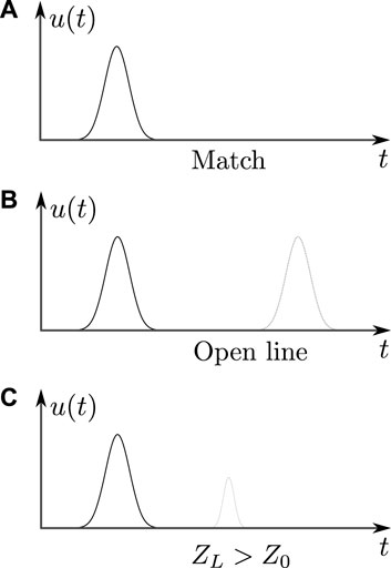
FIGURE 1. Selected reflection pulse behaviors of transmission lines. The excitation pulses are drawn in black and the reflected ones in light gray. (A) Matched line, no reflection. (B) Open line. (C) Matched line with an impedance discontinuity ZL inside the line.
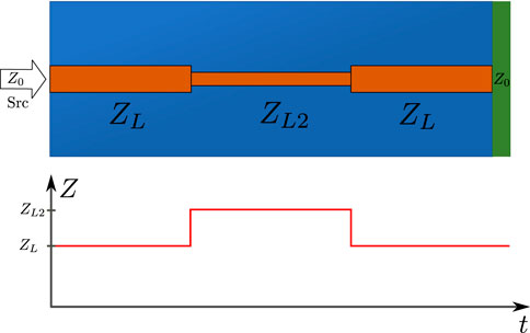
FIGURE 2. Illustration of microstrip trace with segments of different widths, resulting in different characteristic impedance (upper picture). The generator as well as the match have the impedance of the line (Z0 = ZL). The excitation signal is a step function or integral of an impulse. The lower graph resembles the corresponding impedance profile along the line.
The accuracy of the distance measurement mainly depends on the exact knowledge of the propagation velocity (and hence the dielectric behavior). Other aspects which have to be taken into account in practice are the sampling properties of the receiver. The spatial resolution, namely, the accuracy to tell apart two closely spaced discontinuities, is correlated to the propagation time between their two locations and the system rise time and is given by (4) (Tektronix, 2007):
However, there are even more accuracy degrading factors (e.g., unwanted reflections), which can be reduced using appropriate signal processing (Dunsmore, 2012). Other related methods for reflectometric measurements not discussed here are frequency-domain reflectometry, where a frequency sweep is being applied to the device under test and the result is being transformed back to the time-domain using inverse Fourier transform as well as spread-spectrum time-domain reflectometry.
Applying the idea of not only measuring the conductance of a trace but also the characteristic impedance at any place (and of course also complete interruptions) adds some new interesting insights into the detection principle. Partly damaged traces can be detected, since a change in the trace width and alteration in the surrounding dielectric lead to a different characteristic wave impedance at that exact position. For an exposed conductor system, there might also be the possibility to detect micro-abrasion and degradation over time caused by very small MMSD. Figure 3 displays an example of one detection layer. Impacts 1 and 2 cannot be detected and localized using the continuity or resistive method, but the reflectometric approach makes these damages visible. Impacts 3 and 4 share a common partly damaged line, which would be invisible in the continuity testing method and therefore reduce the estimated size of the impact.

FIGURE 3. Partly damaged PCB traces can still serve detection purposes: impact (2) can still be detected, even if the same traces are already damaged by impact (1). Impacts (3) and (4) share a common damaged line; their locations on the line can also be recognized. Generator/evaluation unit and/or terminations are not displayed in the picture for clarity.
Existing wire- or PCB trace-based detectors utilizing a continuity test are only able to detect a single impact per trace or a resistance change of the entire line. If the trace is completely damaged once, no current for measurement can flow anymore. The proposed reflectometric method is able to still detect the impact if there are already previous damages along the line, and also partial impacts can be detected. If one of the considered single detection layers is connected to an evaluation unit at only one side, it is possible to detect one to two complete impacts which cut the line completely. This is the case if the second impact is located closer to the evaluation circuit. Depending on the specific setup, namely, evaluating the reflections from both sides of the grid, there is even the possibility to detect a minimum of two and up to four total impacts per line. Figure 4 shows an exemplary setup of a double-layered detection grid with reflectometric evaluation from one side each, while the other side is terminated. Considering only the vertical lines and that impact one took place before impact 3, the alteration of the impedance profile can still be detected. The same is the case for the horizontal lines if impact 2 happened before impact 3. As a consequence, the position of impact 3 can be completely determined, even though the traces have been completely cut before.
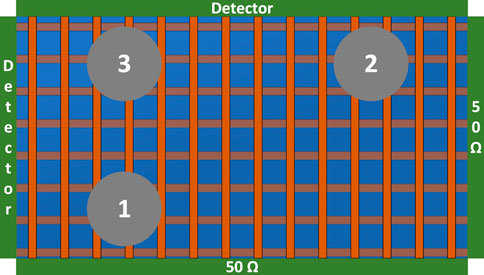
FIGURE 4. Resistive grid (continuity testing) would not be able to detect impact (3) after impacts (1) and (2). The use of a technique based on reflectometry could avoid this “blind spot” along already broken traces.
A double-layered conductor grid with perpendicularly arranged traces has been used, for e.g., in SOLID, and is necessary for the exact determination of an impact site in two dimensions. The novel concept presented in this article could also support the usage of only one detection layer (with some limitations). A use-case could be if there are some constraints regarding complexity or cost. However, this goes along with a limited detection capability. If the evaluation circuit is only connected to one side of the grid, it might be possible to detect an impact position and also measure the shape and size of an object in the y direction. Also, a second impact detection on the very same lines is possible, if this one is located closer to the evaluation circuit than the previous impact. With the connection of such a circuit on both sides of the detection grid, we again get the possibility to characterize an impact from both sides. A second impact and third impact can be detected and partly characterized (from one side) if located closer to one of the detection circuits.
Similar to already existing systems, a multitude of traces have to be merged to be driven by the main evaluation unit using switching devices like multiplexers. In this case, since we are dealing with high frequencies and fast pulses, suitable devices like DC-compatible microelectromechanical system (MEMS) switches have to be used. To minimize the number of channels, also meander-shaped structures are imaginable since the concept can distinguish the areas between the bends. The reflectometric method can also be used in addition and on top of the traditional and more simple evaluation concept since also DC-compatible multiplexers are used here. This adds a secondary layer of redundancy.
In this section, CAE software CST (Dassault Systemes CST Studio Suite, 2022) has been used. The software application is a so-called full-wave numerical electromagnetic simulator, which discretizes a 3D model and simulates the electromagnetic behavior including material characteristics and coupling. Multiple solvers are available for different use-cases, such as time-domain, frequency-domain, or eigenmodes. For the following simulations, the time-domain solver has been used. Numerous simulations with damaged and partly damaged single lines and different excitation signals have been conducted. Exemplarily, the following microstrip transmission line PCB has been modeled. Figure 5 shows a microstrip line with a length L of 150 mm and a trace width w of 0.45 mm with two holes, each with a diameter of 2 mm. The hole displayed on the left side cuts away half of the trace width, whereas the hole on the right side has been moved between different positions in the vertical position. In the first position, the hole just touches the trace at its lateral side and then moves further inside until it is completely cut. The system is being fed from the left side and terminated from the right, and the equivalent pulse rise time (10–90%) tr is around 44 ps. The resulting curve shows the impedance along the time, whereas the latter one directly corresponds to the position along the line, considering the propagation velocity. It can be seen that the further the second hole moves inside the trace area, the higher its characteristic impedance gets. So a direct relationship between the intrusion depth of a hole and the resulting impedance is given. To demonstrate the effect of the detectability of an impact, even if the trace has already been partially hit before, the hole in the center has been introduced. Vice versa, even if the hole on the right side completely cuts the trace, the first hole can still be detected.
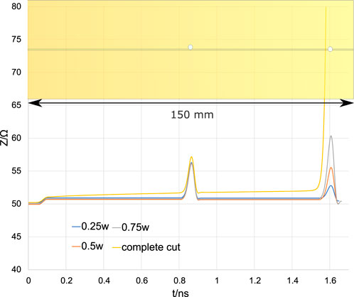
FIGURE 5. Illustration of an impedance curve for different hole indentations of the right hole. The overlay shows the corresponding holes in the microstrip, and the right one in the position of a complete trace cut. The microstrip itself is being fed from the left-hand side, and the right-hand side is terminated.
To validate the simulation results and to get an impression of how accurate different measurement methods tend to be, various measurements have been carried out. A 304.8 mm long microstrip line on top of a 1.27 mm thick Rogers TMM3 PCB and a nominal strip width of 2.88 mm have been fabricated. This results in a characteristic impedance of 50 Ω. The rather large strip width of the first prototypes has been chosen for practical and production reasons (thickness) and to achieve good results even with manual machining/drilling. It is proposed that later versions feature much narrower strips. The PCB is equipped with two SMA-style soldering connectors.For the measurement of the line properties and its characterization, two different devices relying on different measurement principles and in varying price ranges have been used: a Rohde & Schwarz ZVB20 vector network analyzer with a time-domain option (20 GHz, FDR) and a USB-driven Sympuls TDR meter (80 ps rise time). After calibration of the devices, the reference plane had to be evaluated to exclude parts of the test fixture/connectors. For this purpose, a custom-made short was used. For the measurement of the PCB itself, the second port of the PCB trace has been terminated with 50 Ω. The computer simulation was configured to roughly have the same behavior as the vector network analyzer (fmax = 20 GHz). This again is equivalent to a pulse rise time (10–90%) of around 44 ps.
After the first measurement of the line without any perturbation, holes of 1, 2, and 3 mm diameter have been drilled in the exact half of the board (at position 15.24 cm) and centered on the edge of the trace and just covering half of it (see Figure 6).
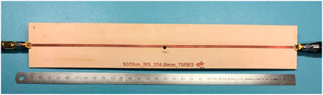
FIGURE 6. Photograph of measured microstrip PCB trace with the offset hole in the center of the PCB. The board is being fed from the right-hand side.
In addition, computer simulations with the same PCB and hole setup have been made in CST Studio for comparison. The results of both measurements and the corresponding simulation are shown in Figure 7 and Table 1. The distance has been calculated from the average dielectric constant ϵr, eff given in the datasheet.
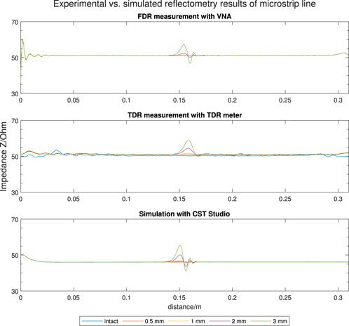
FIGURE 7. Measured and simulated reflectometry results of microstrip line impedance with different hole sizes at the center location. The physical position is 15.24 cm. The hole covers half of the strip laterally.
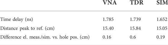
TABLE 1. Time delays and resulting distance calculated with the average ϵr of TMM3 material between the assumed reference plane and the TDR peak position. Also given is the difference of measured/simulated value vs. physical hole position (15.24 cm).
It can also be seen that the first and third graphs have a quite good match regarding their TDR responses. One can draw a conclusion from the response curve to hole size. The second graph, recorded with the cost-efficient TDR meter, has a coarser spatial resolution. Even though the 1 mm hole (respectively half of it) can only be detected hardly, larger holes can be clearly distinguished. But it has to be mentioned again that the used strip width for practical use is intended to be much narrower in future prototypes, which shall lead to more responsivity even for a small impact.
Although the devices have all been calibrated to a reference plane and the delay values respective distances offset to remove the fixture, there is still quite a small time/distance deviation between the graphs. This is because the calibration plane could not often be determined very exactly, due to a not well-defined impedance and therefore the electrical length of the soldered connectors. This could be improved by the use of high-grade solderless measurement-grade connectors for the prototype and introducing reference features at the PCB level to conduct differential distance measurements, also for calibration.
The impedance, as well as the distance calculation for the graph, has been calculated with the nominal value for the dielectric constant, given in the datasheet of the TMM3 material of ϵr = 3.27 ± 0.032 (mentioned previously). The given tolerance can be neglected for the impedance since it leads to insignificant changes in the decimal place. However, a tolerance of the dielectric constant could lead to an impact on the total spatial accuracy. Calculated for a reflection at 1.5 ns, the deviation can be in the millimeter range. But assuming an evenly distributed and well-defined dielectric constant of a specific PCB lot combined with an exact calibration, this possible inaccuracy could be reduced.
In the following measurement, the same setup which has been used previously was utilized, but in this case, the PCB trace features two holes with a spacing of 70 mm (Figure 8). The first one has a diameter of 3 mm and the second one of 2 mm, each positioned on the edge of the PCB trace. This experiment shall demonstrate the capability to detect not only multiple perturbations but also the possible accuracy if the ambiguous impedance and length of a soldered standard PCB connector are not taken into account. Alongside the measurement, a simulation has been conducted as well. The results are shown in Figure 9 and Table 2.
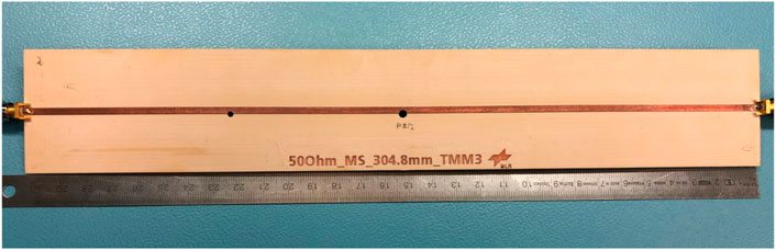
FIGURE 8. Photograph of measured microstrip PCB trace with two offset holes of different sizes in the center of the PCB, 7 cm apart. The board is being fed from the right-hand side.
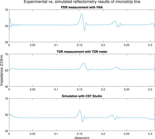
FIGURE 9. Measured and simulated reflectometry results of microstrip line impedance with two different holes (3 and 2 mm diameter) at the center location and 7 cm apart. The holes cover half of the strip laterally.
TABLE 2. Time delays and resulting distance were calculated with reference ϵr between the two perturbation maxima for the two measurement devices and the computer simulation.
The outcome shows that the two holes can be clearly distinguished in both graphs. Furthermore, it can be seen that the distance inaccuracy shown in the previous section could be drastically reduced due to the relative measurement on PCB. This strengthens the assumption that this can be attributed to inaccurate knowledge of the electrical length of the SMA solder connector. However, the simulation has the largest deviation from the true value, and this might have its root cause due to the discrete nature of the mesh and is a matter of further investigation.
In this article, a novel concept for an improved conductive trace-based in situ space debris detector is presented. With this concept, even more information about the impact can be collected compared to existing approaches. Completely cut as well as partially damaged lines can be, depending on the case, used multiple times, and impact types can be distinguished from each other. The reflectometry approach could be used in addition to the common methods, but it offers the option to reduce the layer complexity at the detection site as well. The upcoming miniaturized RF COTS parts of the last couple of years could enable the practical implementation of a compact onboard-reflectometer including the necessary RF routing network. First prototypes have been fabricated and evaluated with different measurement methods, which showed promising results. Even with lower-cost commercial measurement equipment and longer pulse rise times (and thus reduced cost and complexity), characteristics of the impact of different sizes can be seen. Future work on the project will also include more in-depth analysis of thinner lines to improve detection capabilities for small impactors. This shall also cover multi-line boards regarding their its RF behavior, such as line coupling and resonance and the corresponding calibration strategy. An important figure of merit will also be the achievable accuracy of the measurements, both in simulation and practice and under different circumstances (materials and environment). Also, a suitable material for lamination into the structure of a solar panel has to be evaluated. The used substrate material has to be carefully chosen for a stable dielectric constant. However, temperature compensation techniques will be unavoidable to improve accuracy. The detection concept and system have been patented under Hauer et al. (2018) and Hauer and Fexer (2017). These patents include the idea to integrate such a detection concept into certain antenna types (e.g., wire or spiral antennas) and to monitor the impact on these kinds of structures. Also, possible RF COTS parts are under investigation and being sourced.
The raw data supporting the conclusion of this article will be made available by the authors, without undue reservation.
The author confirms being the sole contributor of this work and has approved it for publication.
The author declares that the research was conducted in the absence of any commercial or financial relationships that could be construed as a potential conflict of interest.
All claims expressed in this article are solely those of the authors and do not necessarily represent those of their affiliated organizations, or those of the publisher, the editors, and the reviewers. Any product that may be evaluated in this article, or claim that may be made by its manufacturer, is not guaranteed or endorsed by the publisher.
Bauer, W., and Romberg, O., (2016). “Debris in-situ impact detection by utilization of cube-sat solar panels (4S Symposium),” in Proceedings of the Small Satellites, Systems & Services (4S) Symposium, Valletta, Malta.
Bilén, S. G., and Gilchrist, B. E. (2001). Electrodynamic-tether time-domain reflectometer for analyzing tether faults and degradation. AIP Conf. Proc. 552, 461–466. doi:10.1063/1.1357962
Bishop, J. A., Pommerenke, D. J., and Chen, G. (2011). A rapid-acquisition electrical time-domain reflectometer for dynamic structure analysis. IEEE Trans. Instrum. Meas. 60, 655–661. doi:10.1109/TIM.2010.2058551
Bunte, K. D., and Jurke, K.-N., (2021). “Data of European in-situ impact detectors for environment model validation,” in Proceedings of the 8th European Conference on Space Debris (ESA Space Debris Office).
Dassault Systemes CST Studio Suite (2022). Electromagnetic field simulation software. Available at: https://www.3ds.com/products-services/simulia/products/cst-studio-suite/(Accessed 07 23, 2022).
Dunsmore, J. P. (2012). Handbook of microwave component measurements (3rd Edition 2014,). John Wiley & Sons Ltd, Chichester, West Sussex, United Kingdom.
Furse, C., and Haupt, R. (2001). Down to the wire [aircraft wiring]. IEEE Spectr. 38, 34–39. doi:10.1109/6.898797
Furse, C., Smith, P., and Diamond, M. (2009). Feasibility of reflectometry for nondestructive evaluation of prestressed concrete anchors. IEEE Sens. J. 9, 1322–1329. doi:10.1109/JSEN.2009.2019309
Hamilton, J., and Liou, J.-C. (2017). “Development of the space debris sensor,” in Proceedings of the 7th European Conference on Space Debris (ESA Space Debris Office).
Hammerstad, E., and Jensen, O. (1980). Accurate models for microstrip computer-aided design. IEEE MTT-S Int. Microw. Symp. Dig., 407–409. doi:10.1109/MWSYM.1980.1124303
Hiebel, M. (2006). Grundlagen der vektoriellen Netzwerkanalyse. (3rd. Edition 2011). Munich: Rohde & Schwarz GmbH&Co. KG.
Kitazawa, Y., and Sakurai, A. (2009). “Development of a new type sensor for in-situ space debris measurement,” in IAC-09.A6.1.9 (International Astronautical Congress).
Kuitunen, J., and Drolshagen, G. (2001). “Debie - first standard in-situ debris monitoring instrument,” in Proceedings of the Third European Conference on Space Debris (ESA Space Debris Office), 185–190.
Ledieu, J., De Ridder, P., De Clerck, P., and Dautrebande, S. (1986). A method of measuring soil moisture by time-domain reflectometry. J. Hydrology 88, 319–328. doi:10.1016/0022-1694(86)90097-1
Menicucci, A., and Drolshagen, G. (2013). “Flight and post-flight impact data analysis from DEBIE2 (debris in-orbit evaluator) on board of ISS,” in Proceedings of the 6th European Conference on Space Debris (ESA Space Debris Office).
Shumaker, B. D., Campbell, C. J., Sexton, C. D., Morton, G. W., McConkey, J. B., and Hashemian, H. M. (2012). in Cable condition monitoring for nuclear power plants 2012 Future of Instrumentation International Workshop (FIIW) Proceedings, 1–4. doi:10.1109/FIIW.2012.6378325
Tektronix (2007). TDR impedance measurements: A Foundation for Signal Integrity. Beaverton, Oregon: Tektronix Inc.
Todoroki, A., Kurokawa, H., Mizutani, Y., Matsuzaki, R., and Yasuoka, T. (2014). Self-sensing time domain reflectometry method for damage monitoring of a cfrp plate using a narrow-strip transmission line. Compos. Part B Eng. 58, 59–65. doi:10.1016/j.compositesb.2013.10.047
Keywords: space debris, micrometeoroid, in situ, detector, reflectometry, time domain reflectometry
Citation: Fexer S (2022) A novel evaluation method for in situ space debris detection based on conductive traces. Front. Space Technol. 3:867853. doi: 10.3389/frspt.2022.867853
Received: 01 February 2022; Accepted: 19 August 2022;
Published: 21 October 2022.
Edited by:
Vitali Braun, IMS Space Consultancy, GermanyReviewed by:
Wensheng Huang, National Aeronautics and Space Administration (NASA), United StatesCopyright © 2022 Fexer. This is an open-access article distributed under the terms of the Creative Commons Attribution License (CC BY). The use, distribution or reproduction in other forums is permitted, provided the original author(s) and the copyright owner(s) are credited and that the original publication in this journal is cited, in accordance with accepted academic practice. No use, distribution or reproduction is permitted which does not comply with these terms.
*Correspondence: Sebastian Fexer, c2ViYXN0aWFuLmZleGVyQGRsci5kZQ==
Disclaimer: All claims expressed in this article are solely those of the authors and do not necessarily represent those of their affiliated organizations, or those of the publisher, the editors and the reviewers. Any product that may be evaluated in this article or claim that may be made by its manufacturer is not guaranteed or endorsed by the publisher.
Research integrity at Frontiers
Learn more about the work of our research integrity team to safeguard the quality of each article we publish.