
95% of researchers rate our articles as excellent or good
Learn more about the work of our research integrity team to safeguard the quality of each article we publish.
Find out more
ORIGINAL RESEARCH article
Front. Phys. , 20 January 2025
Sec. Chemical Physics and Physical Chemistry
Volume 12 - 2024 | https://doi.org/10.3389/fphy.2024.1534301
This article is part of the Research Topic Calculation and Design of Two-dimensional Thermoelectric and Piezoelectric Materials, Volume II View all articles
 Xiuzhi Du1
 Zhaoming Huang2*
Two-dimensional (2D) materials present novel electronic and catalytic performances, showing a promising application as nano-device. In this investigation, a family of 2D material, X2B6 (X = K, Na and Rb), is predicted with puckered crystal structure by elemental mutation method. The dynamic and thermal stability of the X2B6 monolayer is addressed. The anisotropic mechanical properties of the X2B6 monolayer is obtained by the Young’s modulus (296–406 N/m) and the Poisson’s ratio (0.36–0.35). Interestingly, the K2B6 and Rb2B6 monolayers demonstrate a metallic band structure, while the Na2B6 monolayer is a semiconductor with an ultra-narrow bandgap only about 0.42 eV. Then, the ultra-high electron mobility in the Na2B6 monolayer is calculated as about 9942 cm2.V−1.s−1, and the excellent optical performance of the Na2B6 monolayer is also addressed. More importantly, the advantageous catalytic activity in hydrogen evolution reduction (HER) and oxygen evolution reactions (OER) is explored in these X2B6 monolayers. Our work suggests a theoretical guidance to use the X2B6 monolayer as a high-speed electronic devices and highly efficient catalyst.
2D materials have attracted considerable focus after the preparation of the graphene [1], which shows the excellent thermal and catalytic performances [2–4]. While the zero bandgap limits the application of graphene in power devices [5, 6], and then the transition metal dichalcogenides (TMDs) materials are proposed with decent bandgaps larger than that of the bulk one [7]. For example, the MoS2 monolayer presents novel optical absorption characteristics as a potential photocatalyst [8, 9], which also can be prepared as photoluminescence [10]. In particular, the Janus MoSSe monolayer, as popular asymmetric TMDs, further demonstrates a novel thermal and phononic properties with a polar nature [11–13]. Likewise, 2D Janus materials explain different characteristic on both sides, such as adsorbed [14], catalytic [15], mechanical [16] and electronic properties [17]. All these obtained novel performances of the 2D materials also can be tuned by strain engineering [18, 19], interface coupling [20, 21], external electric field [22] and temperature [23] etc.
Using the nanoscale materials as a catalyst in the hydrogen evolution reaction (HER) and oxygen evolution reaction (OER) is also popular [24–26], because more active sites can be exposed [27–30]. For example, the ability of the OER of the CoO2 and FeO2 monolayers can be improved by decreasing 40% overpotential under external strain [31]. The barrier of the biphenylene network in HER is obtained as low as −0.03 eV by the decent atomic doping [32]. The intrinsic defect is also a popular strategy to tune the HER and OER performances of the 2D materials [33]. Besides, to further extend the application range of 2D material, the heterostructure is constructed, which can induce novel electronic and catalytic properties because of the built-in electric field across the interface [17]. PtS2/arsenene heterostructure is constructed with a −0.487 eV potential for the HER, which is lower than the origin PtS2 and arsenene monolayers [34]. C2N/WS2 heterostructure can facilitates OER with potential of about 1.81 eV [35]. Besides, the prediction of new 2D materials is also an important approach to expand the properties for nano-devices [36, 37]. For example, Ag2S monolayer acts a semiconductor with auxetic mechanical properties using as nano-electronics [38]. The band edge positions of the SnP2S6 monolayer promises the redox potential of the water splitting as a photocatalyst [39]. IV–VI monolayers present ultrahigh carrier mobility, which also act as an excellent HER catalyst [40]. Recently, 2D boron based compound has been proposed to possess excellent electronic and catalytic properties. For example, the Janus B2P6 is predicted as potential photocatalyst for water splitting [41], and the band edge energy also can be tuned by external strain [42]. The Li2B2 monolayer is calculated with a high hole mobility of 6.8 × 103 cm2⋅V− 1⋅s− 1 using as high-speed electronic devices [43]. The auxetic B4N monolayer shows an apparent mechanical anisotropy coupled with robust structural stability in future nano-mechanical devices [44]. All these point that exploring the boron (B) based 2D materials as advanced functional material presents significant prospects.
In this work, we propose a novel 2D materials, X2B6 (X = K, Na and Rb) monolayer, using elemental mutation method by the prototype of Li2B6 monolayer [43]. The stability of the predicted K2B6, Na2B6 and Rb2B6 monolayers is addressed by phonon spectrum and the ab initio molecular dynamics (AIMD) simulations. The mechanical and the electronic performances are investigated by the density functional theory (DFT). Then, the ultra-high electron mobility and the optical light absorption properties are obtained in the Na2B6 monolayer. The unique catalytic activity of these X2B6 monolayer in HER and OER is studied.
All the calculations in this investigation were implemented by Vienna ab initio simulation package (VASP) using first-principle method, which is based on the DFT [45–47]. The core electrons was addressed in the simulations using projector augmented wave potentials (PAW) [48, 49]. The Perdew–Burke–Ernzerhof (PBE) was carried out to demonstrate the exchange correlation method based on the generalized gradient approximation [50–52]. To correct the weak van der Waals interaction in the HER and OER system, the DFT-D3 method was used by Grimme functional [53]. Furthermore, the Heyd–Scuseria–Ernzerhof (HSE06) calculations were explored to investigate the electronic and optical performances of the Na2B6 monolayer [54]. It is worth noting that the spin effect was not taken into account in the calculation of electronic properties, because we found that the obtained band structure with the spin turned on and off are exactly the same, shown as Supplementary Figure S1. The Monkhorst–Pack with a k-point grids as 11 × 11 × 1 and 17 × 17 × 1 were used in the relaxation and self-consistent simulations, respectively. The vacuum space was set as 25 Å, which can optimize the interaction of nearby layers. The parameter of the convergence for force and energy are set as 0.01 eVÅ−1 and 0.01 meV, respectively. In the simulation of the phonon spectra, the PHONOPY code was used based on the density functional perturbation theory [55, 56].
First, the atomic structure of the K2B6, Na2B6 and Rb2B6 monolayers are predicted with the puckered crystal structure showing a space group of Pca21, by elemental mutation method using the prototype of structure from the Li2B6 monolayer [43]. The optimized structure of the X2B6 monolayer is presented as Figure 1A and the obtained lattice parameters of the a (or b) in unit-cell of the K2B6, Na2B6 and Rb2B6 monolayers are 4.311 (or 3.554), 4.313 (or 3.616) Å and 4.312 (or 3.552) Å, respectively, which is smaller than that of the Li2B6 monolayer. The bond length of X–B (LXB) and the B–B (LBB) in the K2B6, Na2B6 and Rb2B6 monolayers are obtained as LXB = 2.850 Å and LBB = 5.018 Å, LXB = 2.523 Å and LBB = 3.598 Å, LXB = 2.978 Å and LBB = 5.450 Å, respectively. Furthermore, the cohesive energy of the K2B6, Na2B6 and Rb2B6 monolayers is calculated as 6.794 eV/atom, 5.974 eV/atom and 6.048 eV/atom, respectively, which is obtained by (2EX + 6EB–EXB)/8, where EX, EB and EXB are used to present the total energy of an X, B atoms and the X2B6 system, respectively. Thus, the calculated cohesive energy of the X2B6 system is also larger than that the predicted IV–VI system (about 3.37–3.81 eV/atom) [57] and comparable with the CB monolayer (about 6.13 eV/atom) [58], showing a stability for these K2B6, Na2B6 and Rb2B6 monolayers. Besides, the dynamic stability of the K2B6, Na2B6 and Rb2B6 monolayers is also studied by phonon spectra obtained in Figure 1B. Obviously, no imaginary frequency can be found in the phonon spectra of these X2B6 monolayer, suggesting the dynamic stability of the K2B6, Na2B6 and Rb2B6 monolayers. The highest frequency of the optical branch of the K2B6, Na2B6 and Rb2B6 monolayers is about 34 THz which is smaller than the prototype of the Li2B6 system.
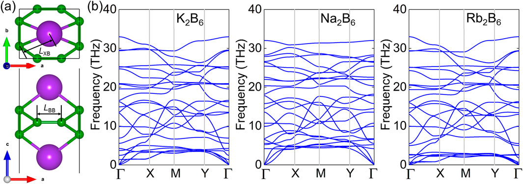
Figure 1. (A) The crystal structure and the (B) phonon spectrum of the X2B6 monolayer. The green and the purple atoms are B and X atoms, respectively.
Then, the thermal stability of the K2B6, Na2B6 and Rb2B6 monolayers is also investigated by the AIMD method by the Nosé−Hoover heat bath functional [59]. The supercell of the X2B6 monolayer is obtained as 7 × 4 × 1 to prevent the lattice translational constraints, which also presents 192 atoms [60]. Besides, the structure of the X2B6 monolayer is totally relaxed under 300 K and 600 K for 10 ps, after the complete calculations. One can see that the crystal structure of the X2B6 monolayer is still undamaged shown as the insets of Figure 2. The temperature and energy of the X2B6 monolayer system in the AIMD calculations are also convergent demonstrated as Figure 2, explaining a clear thermal stability at 300 K. Furthermore, the K2B6 and Na2B6 monolayers are also stable at 600 K because the structure is still intact, while the structure of the Rb2B6 monolayer can be melted down at 600 K, shown as Figure 2.
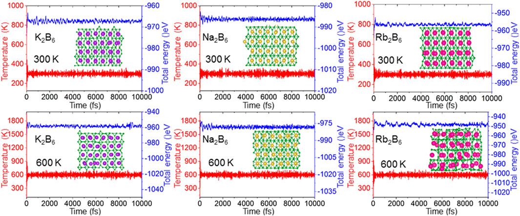
Figure 2. The energy and the temperature of the X2B6 monolayer in the AIMD calculations, the inset is the relaxed structure of the X2B6 monolayer at 300 K and 600 K for 10 ps.
Then, the mechanical properties of these X2B6 monolayer is investigated by the orientation dependences of Young’s modulus using [61] Equation 1 as follows:
where θ explains the angle of a direction shown as Figure 1A. The calculated Young’s modulus of the K2B6, Na2B6 and Rb2B6 monolayers is demonstrated in Figures 3A, C, E, respectively. One can see that K2B6, Na2B6 and Rb2B6 monolayers present the anisotropic Young’s modulus with the maximal and minimal values at θ = 90° and θ = 0°, respectively, shown as Figures 3A, C, E. The obtained maximal Young’s modulus of the K2B6, Na2B6 and Rb2B6 monolayers are 296 N/m, 397 N/m and 406 N/m, respectively. Then, the orientation dependent Poisson’s ratio of the X2B6 monolayer is also studied by [57] Equation 2 as follows:
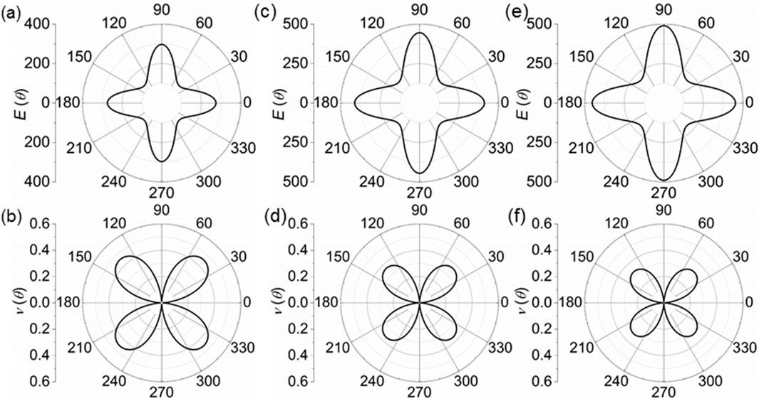
Figure 3. The obtained (A, C, E) Young’s modulus and the (B, D, F) Poisson’s ratio of the (A, B) K2B6, (C, D) Na2B6 and (E, F) Rb2B6 monolayers.
The calculated Poisson’s ratio of the K2B6, Na2B6 and Rb2B6 monolayers are demonstrated by Figures 3B, D, F, respectively. Obviously, the maximal Poisson’s ratio of the K2B6, Na2B6 and Rb2B6 monolayers are obtained as about 0.35, 0.29 and 0.26, respectively, with the θ about 45°. Such obtained Young’s modulus and Poisson’s ratio of the X2B6 monolayer is also higher than that of the carbon monochalcogenides [62] and biphenylene [61].
Furthermore, the band structure of the K2B6, Na2B6 and Rb2B6 monolayers is calculated shown by Figure 4 using PBE method. The K2B6 and Rb2B6 monolayers present a semi-metallic property, shown as Figures 4A, C, while the Na2B6 monolayer suggests semiconductor nature with the direct bandgap that the conduction band minimum (CBM) and the valence band maximum (VBM) are located at the Г point, shown as Figure 4B. In order to obtain a more accurate bandgap of the Na2B6 monolayer, HSE06 functional is explored. Interestingly, the Na2B6 monolayer presents an ultra-narrow bandgap as about 0.42 eV, smaller than the As2X3 system [63], shown as Supplementary Figure S2. It is worth noting that such ultra-narrow bandgap in Na2B6 monolayer is also reported in the PbN/CdO heterostructure (about 0.128 eV) [64], which can serve as a promising efficient nano-electronic and catalyst [65, 66]. Besides, the projected band structure of the Na2B6 monolayer is also demonstrated by Figure 4B. Obviously, B atoms almost contribute to the band energy comparing with the Na atoms.
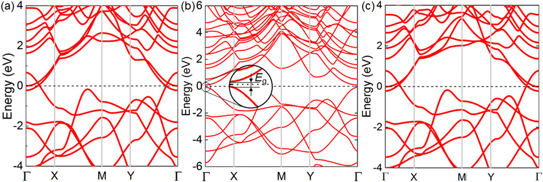
Figure 4. The PBE obtained band structure of the (A) K2B6, (B) Na2B6 and (C) Rb2B6 monolayers. The Fermi level is set as 0 eV.
Since the ultra-narrow bandgap is obtained as about 0.42 eV for the Na2B6 monolayer, the potential application as nano-devices is promising. Thus, the carrier mobility of the Na2B6 monolayer is necessary to be investigated. The electrons and holes mobility of the Na2B6 monolayer along the transport directions (a and b demonstrated in Figure 1A) is explored using the Bardeen-Shockley method [45] which is calculated by Equation 3 as follows:
where elementary charge, the Planck constant and the Boltzmann constant are e, ћ and kB, respectively. The effective mass of the electron and hole is represented using the m*, which is calculated by Equation 4 as follows:
where k and Ek are the wave vector and electronic energy, respectively. C represents the elastic modulus of the monolayered Na2B6, which is obtained by C = [∂2E/∂((l–l0)/l0)/S0. In this equation, the original lattice constant, the free energy and difference of the lattice constant by the strain are expressed as l, E and l0, respectively. S0 is used to represent the area of the Na2B6 monolayer. The energy difference of the Na2B6 system by the external uniaxial strain is calculated as Figure 5A. Furthermore, E is the potential constant of the Na2B6, which is obtained using E = ΔEedge/((l–l0)/l0), where the ΔEedge is difference of the CBM or VBM energy tuned by external strain in the a or b directions. As shown in Figure 5B, the CBM and the VBM of the Na2B6 monolayer can be obviously increased and decreased, respectively, when the external strain is applied. Besides, Figure 5B demonstrates that the dependence of VBM energy of the Na2B6 monolayer is obvious under applied strain, suggesting the large potential constant in the Na2B6 monolayer for holes.
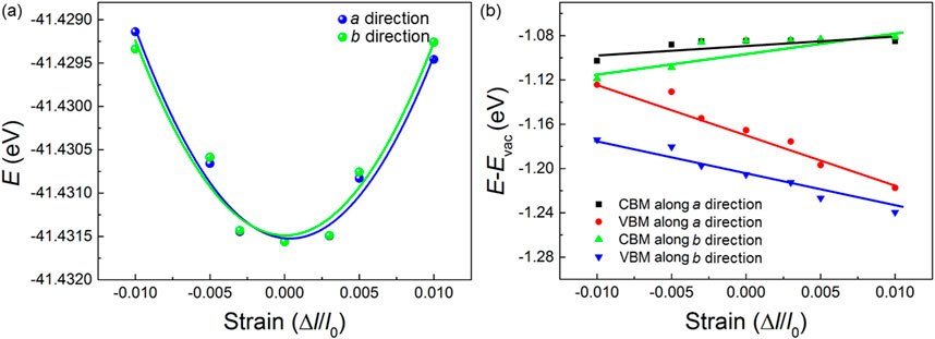
Figure 5. The obtained (A) total and (B) band energy positions of the Na2B6 monolayer under different external strain.
Next, the calculated effective mass of the Na2B6 monolayer along a and b directions are shown as Table 1. One can see that the effective mass of electrons and holes is relatively uniform in transport direction. The calculated deformation potential constant of the hole is larger than that of the electrons in the Na2B6 monolayer shown as Table 1. Besides, the elastic modulus of Na2B6 monolayer is also explained as Table 1. It is worth noting that the elastic modulus of the Na2B6 monolayer is obtained as 409 N.m−1 and 420 N.m−1, respectively, which is consistent with the previous calculation results of Young’s modulus along a and b directions. Therefore, the apparent isotropic carrier mobility of the Na2B6 monolayer is also obtained that electron shows a fast mobility as about 9942 cm2.V−1.s−1 and 5486 cm2.V−1.s−1 along a and b directions, respectively. While the hole mobility in Na2B6 monolayer is calculated as 650 cm2.V−1.s−1 and 862 cm2 V−1 s−1, along a and b directions, respectively. In the same transport direction, the huge difference between electrons and holes allows them to be effectively separated, about 15 (a direction) times and 6 (b direction) times, suggesting the potential application as photocatalyst. Besides, the calculated electron mobility of the Na2B6 monolayer is even higher than that of other 2D materials, such as B2P6 monolayer (5888 cm2.V−1.s−1) [42], Li2B6 monolayer (6800 cm2.V−1.s−1) [43] and MoSi2N4 (2169 cm2.V−1.s−1) [67].
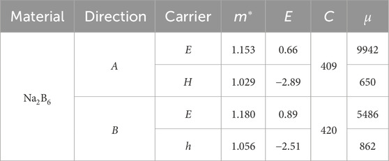
Table 1. The obtained effective mass (m*) and the deformation potential constant (E, eV) of the Na2B6 monolayer. The calculated elastic modulus (C, N·m−1) and carrier mobility (μ, cm2·V−1.s−1) of the Na2B6 monolayer along transport directions.
Considering the ultra-narrow bandgap obtained for semiconductor of the Na2B6 monolayer, the optical absorption spectrum is further calculated by HSE06 method, which is defined as [8] Equation 5 as follows:
where ε1(ω) shows the real parts and the ε2(ω) suggests the imaginary part of the dielectric constant. ω is demonstrating the angular frequency. While the complex dielectric function is calculated by ε(ω) = ε1(ω) + iε2(ω), where ε1 can be calculated from ε2 via the Kramers–Kronig relation. Furthermore, the ε1(ω) and ε2(ω) can be decided as Equation 6 as follows:
where
Shown as Figure 6A, the optical absorption ability is presented that the light absorption peak of the Na2B6 monolayer is about 11.8 × 105 cm−1 with the wavelength about 335 nm. Such excellent optical absorption performance of the Na2B6 monolayer is more advantages than that of other 2D materials such as AlN/Zr2CO2 heterostructure (3.79 × 105 cm−1) [68], CdO/Arsenene heterostructure (8.47 × 104 cm−1) [69] and SiSe monolayer (7.98 × 105 cm−1) [57].
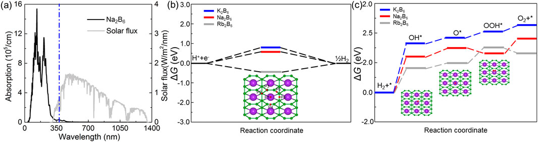
Figure 6. (A) The calculated optical absorption spectrum of the Na2B6 monolayer. The free energy of the in the (B) HER and (C) OER of the K2B6, Na2B6 and Rb2B6 monolayers. The insets represent the structures of the intermediates in the HER and OER.
Then, the catalytic properties of K2B6, Na2B6 and Rb2B6 monolayers are investigated by calculating the Gibb’s free energy of the system. First, the overall process of HER and the OER in water splitting is demonstrated as Equations 7–10 as follows:
where the main reactions in the HER process are:
where * indicates the active site on the Na2B6 monolayer. It can be seen that the intermediate product of the HER process is only H*. As an efficient catalyst, its Gibb’s free energy should satisfy ΔGH = 0 as much as possible. The most excellent Gibb’s free energy in HER of these X2B6 monolayer are obtained as Na2B6 monolayer, shown as Figure 6B, as about 0.64 eV, which is even lower than that of the MoSi2N4 (2.33 eV) [67]. Besides, in the OER reaction, the intermediate products are OH*, O* and OOH*. This process can be expressed as Equations 11–14 as follows:
One can see that the rate-determining step in the OER of the K2B6, Na2B6 and Rb2B6 monolayers is first step with the overpotentials about 1.78 eV, 2.19 eV and 2.28 eV, respectively, shown as Figure 6C. The insets in Figure 6C also demonstrated the adsorption configuration of intermediate. Moreover, the calculated OER catalytic activity of these X2B6 monolayers is also lower than that of the PtS2/arsenene heterostructure (5.516 eV) and WSSe monolayer (2.39 eV). It is worth noting that the most stable HER and OER adsorption configuration of these system is demonstrated by binding energy (Eb), which is obtained as Eb = Esystem–Epure–E, where Esystem, Epure and E are the energy of the adsorbed X2B6, pure X2B6 monolayer and single intermediates, respectively. The lower binding energy imply the more stable configuration of the H*, OH*, O* and OOH*, showing as inset of Figures 6B, C.
In summary, the first-principle calculations are explore to predict the structural, electronic, mechanical, optical and catalytic properties systematically of the novel K2B6, Na2B6 and Rb2B6 monolayers. All these X2B6 monolayers present a stability structure, with an anisotropic Young’s modulus (296–406 N/m) and the Poisson’s ratio (0.36–0.35). Then, the ultra-narrow bandgap (0.42 eV) is obtained in the Na2B6 monolayer with high electron mobility as about 9942 cm2. V−1.s−1. in decent transport direction. Furthermore, the excellent light absorption properties of the Na2B6 monolayer is also investigated. All these X2B6 monolayers suggest a low Gibb’s free energy in HER and OER, suggesting the potential applications as efficient nanodevice and catalyst.
The raw data supporting the conclusions of this article will be made available by the authors, without undue reservation.
XD: Data curation, Formal Analysis, Funding acquisition, Writing–original draft. ZH: Methodology, Software, Supervision, Writing–review and editing.
The author(s) declare that financial support was received for the research, authorship, and/or publication of this article. This work was financially supported by Natural science research project of colleges and universities in Anhui Province (Grant No. 2023AH053094); Key teaching research project of Chuzhou Polytechnic (Grant No. 2022jyxm03).
The authors declare that the research was conducted in the absence of any commercial or financial relationships that could be construed as a potential conflict of interest.
The author(s) declare that no Generative AI was used in the creation of this manuscript.
All claims expressed in this article are solely those of the authors and do not necessarily represent those of their affiliated organizations, or those of the publisher, the editors and the reviewers. Any product that may be evaluated in this article, or claim that may be made by its manufacturer, is not guaranteed or endorsed by the publisher.
The Supplementary Material for this article can be found online at: https://www.frontiersin.org/articles/10.3389/fphy.2024.1534301/full#supplementary-material
2. Ren K, Chen Y, Qin H, Feng W, Zhang G. Graphene/biphenylene heterostructure: interfacial thermal conduction and thermal rectification. Appl Phys Lett (2022) 121:082203. doi:10.1063/5.0100391
3. Wang G, Zhi Y, Bo M, Xiao S, Li Y, Zhao W, et al. 2D hexagonal boron nitride/cadmium sulfide heterostructure as a promising water-splitting photocatalyst. physica status solidi (2020) 257:1900431. doi:10.1002/pssb.201900431
4. Ren K, Liu JZ, Palummo M, Sun M. Editorial: theoretical study of two-dimensional materials for photocatalysis and photovoltaics. Front Chem (2024) 12:1387236. doi:10.3389/fchem.2024.1387236
5. Jariwala D, Sangwan VK, Lauhon LJ, Marks TJ, Hersam MC. Carbon nanomaterials for electronics, optoelectronics, photovoltaics, and sensing. Chem Soc Rev (2013) 42:2824–60. doi:10.1039/c2cs35335k
6. Zhang C, Xu J, Song H, Ren K, Yu ZG, Zhang Y-W. Achieving boron–carbon–nitrogen heterostructures by collision fusion of carbon nanotubes and boron nitride nanotubes. Molecules (2023) 28:4334. doi:10.3390/molecules28114334
7. Zhang H, Chhowalla M, Liu Z. 2D nanomaterials: graphene and transition metal dichalcogenides. Chem Soc Rev (2018) 47:3015–7. doi:10.1039/c8cs90048e
8. Ren K, Sun M, Luo Y, Wang S, Yu J, Tang W. First-principle study of electronic and optical properties of two-dimensional materials-based heterostructures based on transition metal dichalcogenides and boron phosphide. Appl Surf Sci (2019) 476:70–5. doi:10.1016/j.apsusc.2019.01.005
9. Mak KF, Lee C, Hone J, Shan J, Heinz TF. Atomically thin MoS2: a new direct-gap semiconductor. Phys Rev Lett (2010) 105:136805. doi:10.1103/physrevlett.105.136805
10. Splendiani A, Sun L, Zhang Y, Li T, Kim J, Chim C-Y, et al. Emerging photoluminescence in monolayer MoS2. Nano Lett (2010) 10:1271–5. doi:10.1021/nl903868w
11. Ren K, Qin H, Liu H, Chen Y, Liu X, Zhang G. Manipulating interfacial thermal conduction of 2D Janus heterostructure via a thermo-mechanical coupling. Adv Funct Mater (2022) 32:2110846. doi:10.1002/adfm.202110846
12. Qin H, Ren K, Zhang G, Dai Y, Zhang G. Lattice thermal conductivity of Janus MoSSe and WSSe monolayers. Phys Chem Chem Phys (2022) 24:20437–44. doi:10.1039/d2cp01692c
13. Zhang K, Guo Y, Ji Q, Lu AY, Su C, Wang H, et al. Enhancement of van der Waals Interlayer Coupling through Polar Janus MoSSe. J Am Chem Soc (2020) 142:17499–507. doi:10.1021/jacs.0c07051
14. Ren K, Wang K, Zhang G. Atomic adsorption-controlled magnetic properties of a two-dimensional 2D Janus monolayer. ACS Appl Electron Mater (2022) 4:4507–13. doi:10.1021/acsaelm.2c00740
15. Wang G-Z, Chang J-L, Tang W, Xie W, Ang YS. 2D materials and heterostructures for photocatalytic water-splitting: a theoretical perspective. J Phys Phys D Appl Phys (2022) 55:293002. doi:10.1088/1361-6463/ac5771
16. Ren K, Zhang G, Zhang L, Qin H, Zhang G. Ultraflexible two-dimensional Janus heterostructure superlattice: a novel intrinsic wrinkled structure. Nanoscale (2023) 15:8654–61. doi:10.1039/d3nr00429e
17. Zhao L, Huang L, Wang K, Mu W, Wu Q, Ma Z, et al. Mechanical and lattice thermal properties of Si-Ge lateral heterostructures. Molecules (2024) 29:3823. doi:10.3390/molecules29163823
18. Zhang L, Ren K, Li J, Cui Z, Cheng H. The First-Principles Study of External Strain Tuning the Electronic and Optical Properties of the 2D MoTe2/PtS2 van der Waals Heterostructure. Front Chem (2022) 10:934048. doi:10.3389/fchem.2022.934048
19. Wang K, Ren K, Hou Y, Yang D, Zhang G. Strain effects on the magnon-magnon interaction and magnon relaxation time in ferromagnetic CrGeTe3. Phys Rev Appl (2024) 21:054036. doi:10.1103/physrevapplied.21.054036
20. Sun M, Chou J-P, Ren Q, Zhao Y, Yu J, Tang W. Tunable Schottky barrier in van der Waals heterostructures of graphene and g-GaN. Appl Phys Lett (2017) 110:173105. doi:10.1063/1.4982690
21. Luo Y, Wang S, Shu H, Chou J-P, Ren K, Yu J, et al. A MoSSe/blue phosphorene vdw heterostructure with energy conversion efficiency of 19.9% for photocatalytic water splitting. Semiconductor Sci Technology (2020) 35:125008. doi:10.1088/1361-6641/abba40
22. Shu H, Zhao M, Sun M. Theoretical Study of GaN/BP van der Waals Nanocomposites with Strain-Enhanced Electronic and Optical Properties for Optoelectronic Applications. ACS Appl Nano Mater (2019) 2:6482–91. doi:10.1021/acsanm.9b01422
23. Huang L, Ren K, Zhang G, Wan J, Zhang H, Zhang G, et al. Tunable thermal conductivity of two-dimensional SiC nanosheets by grain boundaries: implications for the thermo-mechanical sensor. ACS Appl Nano Mater (2024) 7:15078–85. doi:10.1021/acsanm.4c01803
24. Luo Y, Sun M, Yu J, Schwingenschlögl U. Pd4S3Se3, Pd4S3Te3, and Pd4Se3Te3: candidate two-dimensional Janus materials for photocatalytic water splitting. Chem Mater (2021) 33:4128–34. doi:10.1021/acs.chemmater.1c00812
25. Luo Y, Ren K, Wang S, Chou J-P, Yu J, Sun Z, et al. First-Principles Study on Transition-Metal Dichalcogenide/BSe van der Waals Heterostructures: A Promising Water-Splitting Photocatalyst. J Phys Chem C (2019) 123:22742–51. doi:10.1021/acs.jpcc.9b05581
26. Luo Y, Wang S, Ren K, Chou JP, Yu J, Sun Z, et al. Transition-metal dichalcogenides/Mg(OH)2 van der Waals heterostructures as promising water-splitting photocatalysts: a first-principles study. Phys Chem Chem Phys (2019) 21:1791–6. doi:10.1039/c8cp06960c
27. Wang G, Gong L, Li Z, Wang B, Zhang W, Yuan B, et al. A two-dimensional CdO/CdS heterostructure used for visible light photocatalysis. Phys Chem Chem Phys (2020) 22:9587–92. doi:10.1039/d0cp00876a
28. Wang G, Li Z, Wu W, Guo H, Chen C, Yuan H, et al. A two-dimensional h-BN/C2N heterostructure as a promising metal-free photocatalyst for overall water-splitting. Phys Chem Chem Phys (2020) 22:24446–54. doi:10.1039/d0cp03925j
29. Ye H, Ren K, Wang P, Wang L. The investigation of the NH3-SCR performance of a copper-based AEI-CHA intergrown zeolite catalyst. Front Chem (2022) 10:1069824. doi:10.3389/fchem.2022.1069824
30. Ren K, Leng B, Zhang C, Sun Q, Tang W. The dynamic investigation of intrinsic vibration characteristics of a stranding machine by the finite element method. Front Phys (2023) 11:203. doi:10.3389/fphy.2023.1159064
31. Pu M, Guo Y, Guo W. Strain-mediated oxygen evolution reaction on magnetic two-dimensional monolayers. Nanoscale Horiz (2022) 7:1404–10. doi:10.1039/d2nh00318j
32. Ren K, Shu H, Huo W, Cui Z, Xu Y. Tuning electronic, magnetic and catalytic behaviors of biphenylene network by atomic doping. Nanotechnology (2022) 33:345701. doi:10.1088/1361-6528/ac6f64
33. Ouyang Y, Ling C, Chen Q, Wang Z, Shi L, Wang J. Activating inert basal planes of MoS2 for hydrogen evolution reaction through the formation of different intrinsic defects. Chem Mater (2016) 28:4390–6. doi:10.1021/acs.chemmater.6b01395
34. Ren K, Tang W, Sun M, Cai Y, Cheng Y, Zhang G. A direct Z-scheme PtS2/arsenene van der Waals heterostructure with high photocatalytic water splitting efficiency. Nanoscale (2020) 12:17281–9. doi:10.1039/d0nr02286a
35. Kumar R, Das D, Singh AK. C2N/WS2 van der Waals type-II heterostructure as a promising water splitting photocatalyst. J Catal (2018) 359:143–50. doi:10.1016/j.jcat.2018.01.005
36. Zhu Z, Guan J, Liu D, Tománek D. Designing isoelectronic counterparts to layered group V semiconductors. ACS Nano (2015) 9:8284–90. doi:10.1021/acsnano.5b02742
37. Li R, Cheng Y, Huang W. Recent progress of Janus 2D transition metal chalcogenides: from theory to experiments. Small (2018) 14:1802091. doi:10.1002/smll.201802091
38. Peng R, Ma Y, He Z, Huang B, Kou L, Dai Y. Single-layer Ag2S: a two-dimensional bidirectional auxetic semiconductor. Nano Lett (2019) 19:1227–33. doi:10.1021/acs.nanolett.8b04761
39. Jing Y, Zhou Z, Zhang J, Huang C, Li Y, Wang F. SnP2S6 monolayer: a promising 2D semiconductor for photocatalytic water splitting. Phys Chem Chem Phys (2019) 21:21064–9. doi:10.1039/c9cp04143e
40. Huang Z, Ren K, Zheng R, Wang L, Wang L. Ultrahigh carrier mobility in two-dimensional IV–VI semiconductors for photocatalytic water splitting. Molecules (2023) 28:4126. doi:10.3390/molecules28104126
41. Sun M, Schwingenschlögl U. B2P6: a two-dimensional anisotropic Janus material with potential in photocatalytic water splitting and metal-ion batteries. Chem Mater (2020) 32:4795–800. doi:10.1021/acs.chemmater.0c01536
42. Ren K, Shu H, Huo W, Cui Z, Yu J, Xu Y. Mechanical, electronic and optical properties of a novel B2P6 monolayer: ultrahigh carrier mobility and strong optical absorption. Phys Chem Chem Phys (2021) 23:24915–21. doi:10.1039/d1cp03838a
43. Ren K, Yan Y, Zhang Z, Sun M, Schwingenschlögl U. A family of LixBy monolayers with a wide spectrum of potential applications. Appl Surf Sci (2022) 604:154317. doi:10.1016/j.apsusc.2022.154317
44. Wang B, Wu Q, Zhang Y, Ma L, Wang J. Auxetic B4N monolayer: a promising 2D material with in-plane negative Poisson's ratio and large anisotropic mechanics. ACS Appl Mater Inter (2019) 11:33231–7. doi:10.1021/acsami.9b10472
45. Van de Walle CG, Martin RM. Absolute’’deformation potentials: formulation and ab initio calculations for semiconductors. Phys Rev Lett (1989) 62:2028–31. doi:10.1103/physrevlett.62.2028
46. Capelle K. A bird's-eye view of density-functional theory. Braz J Phys (2006) 36:1318–43. doi:10.1590/s0103-97332006000700035
47. Grimme S, Antony J, Ehrlich S, Krieg H. A consistent and accurate ab initio parametrization of density functional dispersion correction (DFT-D) for the 94 elements H-Pu. J Chem Phys (2010) 132:154104. doi:10.1063/1.3382344
48. Kresse G, Furthmüller J. Efficient iterative schemes for ab initio total-energy calculations using a plane-wave basis set. Phys Rev B (1996) 54:11169–86. doi:10.1103/physrevb.54.11169
49. Kresse G, Joubert D. From ultrasoft pseudopotentials to the projector augmented-wave method. Phys Rev B (1999) 59:1758–75. doi:10.1103/physrevb.59.1758
50. Oganov AR, Glass CW. Crystal structure prediction using ab initio evolutionary techniques: principles and applications. J Chem Phys (2006) 124:244704. doi:10.1063/1.2210932
51. Kresse G, Furthmüller J. Efficiency of ab-initio total energy calculations for metals and semiconductors using a plane-wave basis set. Comp Mater Sci (1996) 6:15–50. doi:10.1016/0927-0256(96)00008-0
52. Perdew JP, Burke K, Ernzerhof M. Generalized gradient approximation made simple. Phys Rev Lett (1996) 77:3865–8. doi:10.1103/physrevlett.77.3865
53. Grimme S. Semiempirical GGA-type density functional constructed with a long-range dispersion correction. J Comput Chem (2006) 27:1787–99. doi:10.1002/jcc.20495
54. Heyd J, Peralta JE, Scuseria GE, Martin RL. Energy band gaps and lattice parameters evaluated with the Heyd-Scuseria-Ernzerhof screened hybrid functional. J Chem Phys (2005) 123:174101. doi:10.1063/1.2085170
55. Togo A, Tanaka I. First principles phonon calculations in materials science. Scripta Materialia (2015) 108:1–5. doi:10.1016/j.scriptamat.2015.07.021
56. Togo A, Oba F, Tanaka I. First-principles calculations of the ferroelastic transition between rutile-type and CaCl2-type SiO2 at high pressures. Phys Rev B (2008) 78:134106. doi:10.1103/physrevb.78.134106
57. Ren K, Ma X, Liu X, Xu Y, Huo W, Li W, et al. Prediction of 2D IV–VI semiconductors: auxetic materials with direct bandgap and strong optical absorption. Nanoscale (2022) 14:8463–73. doi:10.1039/d2nr00818a
58. Ren K, Shu H, Huang L, Wang K, Luo Y, Huo W, et al. Predicted XN (X = C, Si, Ge, and Sn) monolayers with ultrahigh carrier mobility: potential photocatalysts for water splitting. J Phys Chem C (2023) 127:21006–14. doi:10.1021/acs.jpcc.3c06284
59. Nosé S. A unified formulation of the constant temperature molecular dynamics methods. J Chem Phys (1984) 81:511–9. doi:10.1063/1.447334
60. Ren K, Wang S, Luo Y, Chou J-P, Yu J, Tang W, et al. High-efficiency photocatalyst for water splitting: a Janus MoSSe/XN (X = Ga, Al) van der Waals heterostructure. J Phys Phys D Appl Phys (2020) 53:185504. doi:10.1088/1361-6463/ab71ad
61. Luo Y, Ren C, Xu Y, Yu J, Wang S, Sun M. A first principles investigation on the structural, mechanical, electronic, and catalytic properties of biphenylene. Scientific Rep (2021) 11:19008. doi:10.1038/s41598-021-98261-9
62. Sun M, Schwingenschlögl U. Unique omnidirectional negative Poisson’s ratio in δ-phase carbon monochalcogenides. J Phys Chem C (2021) 125:4133–8. doi:10.1021/acs.jpcc.0c11555
63. Fujiwara K, Shibahara M. Thermal transport mechanism at a solid-liquid interface based on the heat flux detected at a subatomic spatial resolution. Phys Rev (2022) 105:034803. doi:10.1103/physreve.105.034803
64. Cheng Z, Wang Y, Zheng R, Mu W. The prediction of two-dimensional PbN: opened bandgap in heterostructure with CdO. Front Chem (2024) 12:1382850. doi:10.3389/fchem.2024.1382850
65. Wang J, Li Y, Deng L, Wei N, Weng Y, Dong S, et al. High-performance photothermal conversion of narrow-bandgap Ti2O3 nanoparticles. Adv Mater (2017) 29:1603730. doi:10.1002/adma.201603730
66. Vo TQ, Kim B. Interface thermal resistance between liquid water and various metallic surfaces. Int J Precision Eng Manufacturing (2015) 16:1341–6. doi:10.1007/s12541-015-0176-0
67. Ren K, Shu H, Wang K, Qin H. Two-dimensional MX2Y4 systems: ultrahigh carrier transport and excellent hydrogen evolution reaction performances. Phys Chem Chem Phys (2023) 25:4519–27. doi:10.1039/d2cp04224j
68. Ren K, Zheng R, Lou J, Yu J, Sun Q, Li J. Ab initio calculations for the electronic, interfacial and optical properties of two-dimensional AlN/Zr2CO2 heterostructure. Front Chem (2021) 9:796695. doi:10.3389/fchem.2021.796695
Keywords: two-dimensional material, X2B6, mobility, catalyst, first-principle calculations
Citation: Du X and Huang Z (2025) The prediction of X2B6 monolayers with ultrahigh carrier mobility. Front. Phys. 12:1534301. doi: 10.3389/fphy.2024.1534301
Received: 25 November 2024; Accepted: 31 December 2024;
Published: 20 January 2025.
Edited by:
Guangzhao Wang, Yangtze Normal University, ChinaReviewed by:
Yi Luo, Jiangsu Ocean Universiity, ChinaCopyright © 2025 Du and Huang. This is an open-access article distributed under the terms of the Creative Commons Attribution License (CC BY). The use, distribution or reproduction in other forums is permitted, provided the original author(s) and the copyright owner(s) are credited and that the original publication in this journal is cited, in accordance with accepted academic practice. No use, distribution or reproduction is permitted which does not comply with these terms.
*Correspondence: Zhaoming Huang, amltbXltYWN5QDE2My5jb20=
Disclaimer: All claims expressed in this article are solely those of the authors and do not necessarily represent those of their affiliated organizations, or those of the publisher, the editors and the reviewers. Any product that may be evaluated in this article or claim that may be made by its manufacturer is not guaranteed or endorsed by the publisher.
Research integrity at Frontiers
Learn more about the work of our research integrity team to safeguard the quality of each article we publish.