
95% of researchers rate our articles as excellent or good
Learn more about the work of our research integrity team to safeguard the quality of each article we publish.
Find out more
REVIEW article
Front. Phys. , 16 June 2022
Sec. Radiation Detectors and Imaging
Volume 10 - 2022 | https://doi.org/10.3389/fphy.2022.872691
This article is part of the Research Topic Novel Ideas for Accelerators, Particle Detection and Data Challenges at Future Colliders View all 17 articles
The WADAPT (Wireless Allowing Data And Power Transmission) consortium has been formed to identify the specific needs of different projects that might benefit from wireless communication technologies with the objective of providing a common platform for research and development in order to optimize effectiveness and cost. Wireless technologies have developed extremely fast over the last decade and are now mature enough to be a promising alternative to cables and optical links, with a possibility of revolutionizing detector design. Although wireless readout has the qualities and properties to be used in many collider detectors, this article focuses on the transmission of large amount of data from vertex detectors at high rate, low power budget and in potential high radiation environment. For vertex detectors, the 60 GHz band has proven to be adequate and commercial products are already available, providing 6 Gbps data links. This technology allows efficient partitioning of detectors in topological regions of interest, with the possibility of adding intelligence on the detector to perform four-dimensional reconstruction of the tracks and vertices online, in order to attach the tracks to their vertex with great efficiency even in difficult experimental conditions, and conveniently substitutes a mass of materials (cables and connectors). Early transceiver module products have been successfully tested for signal confinement, crosstalk, electromagnetic immunity and resistance to radiation. In the long run, emerging 140 GHz bands could also be used for higher data rates (>100 Gbps) at future high energy and luminosity hadron colliders.
The WADAPT consortium [1] chose to firstly investigate the relevance of wireless techniques for data transfer within vertex detectors, where commercially-available products in the 60 GHz band [2] would be adequate. The present ATLAS [3] and CMS [4] experiments have been designed for nominal operation at luminosity of 2 × 1034 cm−2s−1 and 60 interactions per beam crossing. Pileup lead to a number of mismeasured or misidentified tracks, and add extra energy to calorimeter measurements. Pileup confuses the trigger and also the offline reconstruction and interpretation of events. It also increases the execution time for the reconstruction of events in the High Level Trigger and the offline analysis.
The High Luminosity LHC (HL-LHC) is potentially able to deliver a luminosity up to 7.5 × 1034cm−2s−1, increasing the interaction rate and collision pileup beyond existing or envisioned data readout technologies. The detector systems in the experiment will currently need a trigger to sustain a pileup up to 200 interactions per 25 ns beam crossing. The first event selection and data reduction is typically done by a fast trigger decision within 3–6 microseconds after a collision where 40 million events per second are currently reduced to about 100 kHz and at HL-LHC this will be increased by an order of magnitude. In present experiments this decision is based on information from all detector systems except the tracker. For HL-LHC the CMS experiment has developed a data reduction method with pT filtering in the tracker which opens for the use of tracking data in the trigger [5].
The tracker is the most granular detector system in the experiment that is used to associate charged particles with the correct interaction vertices. The tracking detector would ideally read out all information for every single bunch crossing, perform reconstruction in real time, and then apply trigger criteria to filter events or if possible directly process the data in an event filter farm. The challenge is however to read out the very granular detector in time for the fast trigger decision or before data in the pipelined front-end electronics gets overwritten. The data rate needed to read out all hit clusters of 1-2 pixels in the next generation pixel detectors is between 50 and 100 Tbps1. Data from tracking detectors at the two big LHC experiments are today transferred with optical links. The main benefit with optical links compared to wire links is that they are electrically decoupled and free from crosstalk. The weakness of optical links is the size of the connectors, their alignment constrains, and the sensitivity to mechanical damage. Wire/copper links suffer from bandwidth limitation at higher data rates. Furthermore, the tracker is built in a modular way that does not follow the topology of the physics event. The readout is bound to the modularity of the tracker, which is not optimal for a fast trigger decision based on event topology. The advantage of wireless technology is that it is not constrained to the mechanical modularity of the tracker. The technology offers already today data rate comparable with present optical links and no connectors are needed. The next generation of hadron colliders, which might be the envisioned, FCC, would even be more challenging with a peak luminosity of 30 × 1035 cm−2s−1, leading to a pileup up to 1,000 interactions per 25 ns beam crossing, and more granular detectors. Although the current electron-positron colliders do not introduce stringent requirements on the trigger capabilities, the experiments would certainly benefit from the wireless technology. For both types of collider experiments, minimizing the amount of material in the region of the tracking detectors will reduce multiple scattering and nuclear interactions that degrade the precision on the measurement of track momentum and interaction vertices, and in addition will reduce the number of fake hits arising from secondaries. Both CMS and ATLAS upgrades aim at reducing passive material by embedding serial powering [7] or by using DC-DC converters with reduced mass [8].
Well-chosen detector technology and geometry, combined with wireless techniques might help in reducing the amount of cables and optimizing their path, and thus minimizing the geometrical inefficiency. The total or even partial removal of cables and connectors will result in cost reductions, simplified installation and repair, and reductions in detector dead material. These two last aspects are especially important in tracking detectors and they may become particularly important in case of limited access or/and hostile environment.
For a full exploitation of the advantages of integrating a wireless point-to-point readout, new architectures will be necessary.
According to the Shannon-Hartley theorem, the physical data rate at which information can be transmitted over a communication channel is limited by the channel bandwidth and the signal-to-noise ratio2. The fast development of the wireless technologies is linked to the improvements made in the electronics, especially the semiconductor devices and the new simulation capacity [9–15]. This technological evolution is expected to continue in the coming years. Some of the main strategies to improve the performance of radio communication systems are the following:
Over the last decade the spectral efficiency, meaning the data rate of the physical layer that could be transmitted in a given radio frequency bandwidth, has been increased by a factor 100. This efficiency is obtained by the use of higher order modulation coding scheme and multiple data streams (MIMO). The use of these advanced techniques requires intensive digital signal processing, increasing the complexity of the chipset design, the size, as well as the power consumption. The recent progress in terms of computing capability and energy per operation brought by the advanced FinFET and FDSOI technologies comes along with this increase in signal processing complexity, containing the power consumption, heat dissipation and manufacturing cost.
According to the Shannon-Hartley theorem, another strategy to increase the throughput is to increase the spectrum bandwidth. Since the radio frequency frontend and antenna have a bandwidth limited in a proportion of the carrier frequency (typically a maximum of 15–20%), then larger signal bandwidths require transmission at higher frequency, which became feasible, once again, with the progresses made on the electronics.
According to the Free Space Path Loss equation, the attenuation of a 60 GHz transmission at 1 m is about 68 dB, which is 21.6 dB higher than a 5 GHz transmission. Consequently at constant transmit power and using a given modulation scheme, the communication range will be 12 times shorter. This shorter signal range has the benefit that it will mitigate co-channel interference making a high-density channel-reuse design possible.
The higher frequencies lead to smaller sizes of the RF passive components, including antennae, which can be easily integrated into electronic systems. The application-related antenna must be carefully chosen according to many parameters such as directivity/gain, angle aperture, bandwidth, etc. A wide range of antenna topologies can be produced on chip, in package or on advanced printed circuits boards. The use of RF lenses to increase the gain and the directivity of the antenna is also a possibility at this frequency.
Improvements lie in carefully selecting the communication protocol. For a radio communication channel to work, a large amount of the transmission time is devoted to transmitter and receiver synchronisation, medium access, medium sensing, legacy standard-protection mechanism or transmission error compensation. The distribution of a system clock in particle physics detectors will facilitate the transmitter-receiver synchronisation.
Two main transceiver architectures may be considered at mmw frequencies (Figure 1).
Coherent architecture requires precise frequency synthesis (using Phase Locked Loop), and time and frequency synchronization mechanism achieved by digital base-band circuit [16]. This architecture allows complex amplitude and phase modulations, achieving high spectral efficiency, but leads to high power consumption.
On the contrary non-coherent architecture allows amplitude modulation only (On Off Keying, Amplitude Shift Keying or Pulse Amplitude Modulation). The receiver can implement a simple envelope detector, a comparator and digital interface, without any frequency reference or digital base band processing. The quadratic envelope detector provides negative gain, so that the overall receiver noise figure increases and affects the receiver sensitivity. For this reason, this architecture is more dedicated to short range and low power communication.
In the last decade there has been tremendous advances in silicon technologies that have made it possible to build high performance RF transceivers operating in the millimeter-wave (mmw) band. Non- coherent architecture brings high data rate (up to 10 Gbps at 60 GHz) and low power (<10 pJ/bit) for short-range applications [17]. Recent advance in antenna and packaging design allows the integration of the mmw antenna on chip [17] or in package [18] with good efficiency. Commercial products are now available for mass market applications with 3 main competitors (Lattice (SiBeam), Molex (Keyssa) and STMicroelectronics (Figure 2), proposing different integration schemes function of the application. Strong efforts have also been put on the compatibility with high/low speed digital protocols (USB3, PCIe, Gig Ethernet, UART) for a seamless cable replacement. In parallel a HEP dedicated 60 GHz Integrated Chip was under development in Heidelberg, using 130 nm SiGe BICMOS technology [19] in order to assess the feasibility and performance of the wireless link and establish solid foundation for designing the final reading system. The first prototype was designed to handle a data rate of 4.5 Gbps over a link distance of 1 m. Estimated power consumption for a first full prototype readout is about 150 mW.
Research is progressing [20] towards very high data rate wireless communication systems, using channel aggregation or channel bonding in W or D-band (110–170 GHz), where huge bandwidths (35 GHz aggregated) are available for short range communications. Channel bonding is particularly relevant for the aggregation of data from multiple detectors. A total of 16 channels of 7 Gbps each can be aggregated in a D-band transceiver, reaching 100 Gbps. The data can be sent over a few tens of meter range using directive planar antennas, such as transmit arrays [21], or over light plastic waveguide material [22].
Possible wireless applications encompass HEP experiments at high-energy colliders, neutrino physics experiments, astroparticle-physics experiments and low energy experiments at the intensity frontier for a large range of particle physics detectors. The first step taken by the WADAPT consortium is to bring the proof of concept in the context of data transmission through a typical vertex detector.
Present and future collider experiments require more and more bandwidth for the handling of ever increasing data rates. It is especially true for highly granular tracking detectors operated at high beam luminosities. The performance is currently limited because of insufficient readout bandwidth. An example is the ATLAS Phase II New Inner Tracker Pixel Detector with five-barrel layers, four end-cap rings and a silicon strip detector with four layers and six end-cap disks, in 1 m radius. The readout should operate at up to 4 MHz (25 µs) L0 rate. At downlink a broadcast trigger and control signal will be sent at 160 Mbps while 10k up-links will transmit data at a rate of 5 Gbps. The data readout problematic, based on wired transmission strategy, is addressed in [23]. Different cabling schemes are evaluated with the goal of 5 Gbps data transmission per cable, while reducing as much as possible the material within the small detector volume. The proposed alternative for future colliders is to replace the innermost dense wired network by a multi-hop point-to-point wireless network, streaming the data radially from the centre to outer enclosure (Figure 3) [24].
The worldwide license-free 60 GHz band (57–66 GHz) [25] is very attractive in order to achieve high data rate transfer.
These features, the high path loss, high material penetration loss, narrow beam-width, Line-Of-Sight (LOS) mode of propagation, and operation in a controlled environment, makes the 60 GHz band optimal for short range operation as in the considered detector, where the signal propagates over a 10 cm distance between layers. In addition, the use of the high carrier frequency translates into small form factor for passives (antenna), which will reduce the material budget. This provides an extremely desirable frequency re-use that can handle a large number of transceivers in a small area as in the HEP detectors and other detector systems. Signal is routed through each layer from the bottom receiver to the transmitter at top side. This multi-hop concept requires that the wave front stay confined between the two considered layers, and does not crosstalks with neighbours.
Feasibility studies regarding the integration of the 60 GHz wireless technologies in silicon tracking detector were performed [26], based on a commercial coherent transceiver from Hittite [27]. Several aspects relevant for the implementation of 60 GHz links were studied: transmission losses, interference effects, absorbing materials and the influence of the antenna design and directivity, power consumption. The results of these studies are reported in Sections 3.1–3.4. More recently, tests have been conducted using non-coherent transceiver prototypes from STMicroelectronics [28], especially for latency, connectivity and radiation hardness.
The data throughput of a wireless read-out system, as depicted in Figure 3, is maximized when links with maximum bandwidth are densely packed. The main challenge is to avoid crosstalk between parallel and subsequent chained links.
Transmission and reflection tests have been performed with a spare silicon strip detector module from the ATLAS barrel detector (Figure 4A). The module is mounted on a 2D movable stage and placed in line of sight of two horn antennas for transmission and reception. The module is irradiated with linearly polarized waves in the range from 57.3 to 61.3 GHz. A spectrum analyzer measures the power transmitted through the module in the radio frequency band without down conversion. The transmitted power is normalized to the power in the absence of module in-between. Figure 4B shows the transmission loss averaged over the chosen frequency band for a few positions along the module.
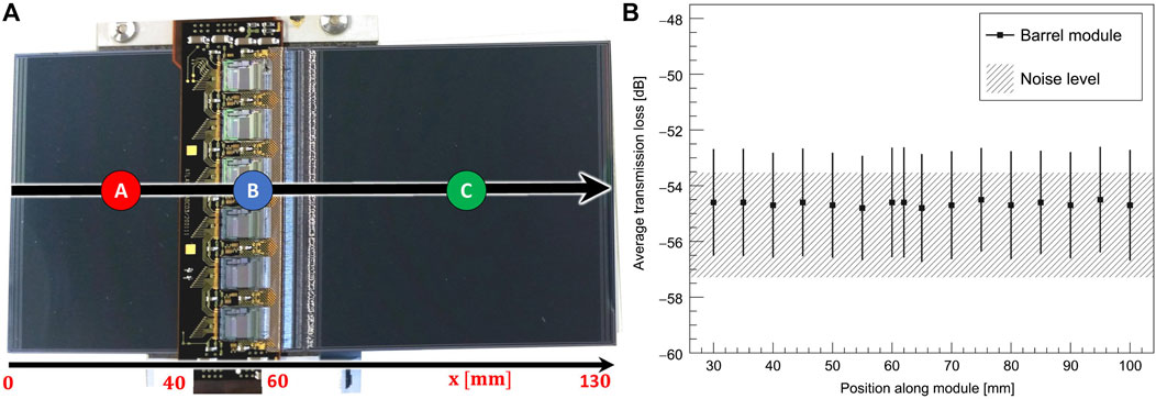
FIGURE 4. (A) The ATLAS SCT barrel module under test. Positions for frequency scans are denoted by (A), (B) and (C). A position scan is performed along the black arrow. (B) Transmission loss of the barrel module averaged over the frequency band for a position scan (along the arrow in panel 4A) and the noise limited sensitivity of the spectrum analyzer. The uncertainties represent the RMS of the average measurements [26].
The measurement is repeated with a spare ATLAS SCT endcap module (Figure 5A). The frequency averaged transmission loss as function of the position on the module (Figure 5B) is −20 dB to −40 dB in the electronics region due to the assembly hole and the gap between hybrid and flex print. As expected the silicon strip region is opaque for the millimeter waves.
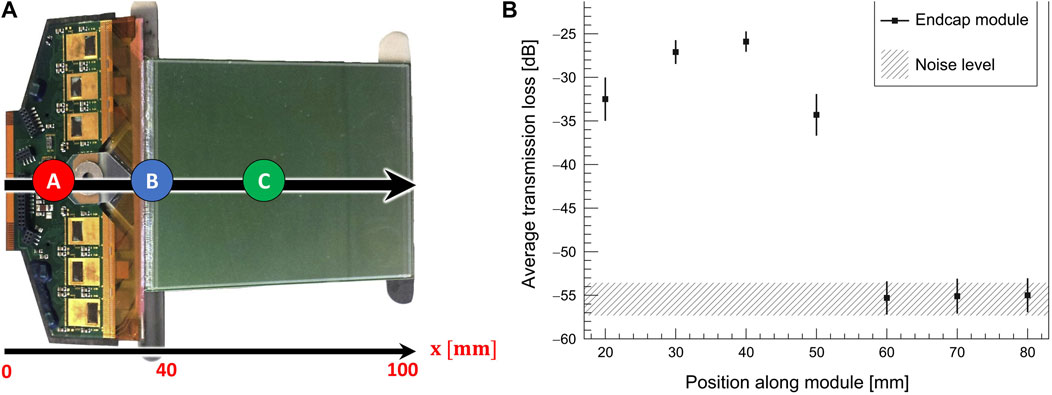
FIGURE 5. (A) The ATLAS SCT endcap module under test. Positions for frequency scans are denoted by (A), (B) and (C). A position scan is performed along the black arrow. (B) Transmission loss of the endcap module averaged over the frequency band for a position scan (along the arrow in panel 5A) [26].
Most of the signal is absorbed by the silicon material, and small reflections may occur due to metallization of the chip and PCB. In some configurations these reflections might induce crosstalk. Absorbing materials (e.g., graphite foam) may be used to attenuate reflections [26].
All wireless links in a tracking detector are installed in stationary positions. Therefore, wireless readout systems can be designed and optimized in order to minimize the interference effects between different links. Nevertheless crosstalk may be an issue for extremely high link densities. However different actions can be combined to reduce crosstalk, if necessary.
One of them is acting on the antenna pattern, using directive antennas with high gain, small beam width and low secondary lobes. By increasing the gain of the antenna, the transmitted power can be decreased while keeping the signal over noise ratio (S/N) in the receiver constant.
In addition the antenna linear or circular polarization direction can be exploited. Crosstalk between adjacent links can be significantly reduced by using orthogonal polarization states.
Furthermore low mass absorbing material can be used to attenuate the spurious reflections without increasing the material budget.
Finally a tunable voltage controlled oscillator (VCO) with sharp filters or low bandwidth antennas may be used to divide the frequency band in different channels. Spreading (CDMA) is also an option with the drawback of reducing the data rate [26].
The different methods for reducing crosstalk discussed in the previous section have been experimentally studied by measuring how close two parallel 60 GHz links can be placed without interfering (Figure 6). The parameter S/N is defined as the ratio of the signals from transmitter #1 (useful signal) over transmitter #2 (interfering signal) measured with the spectrum analyzer at the antenna of the receiver #1. The link quality is considered to be acceptable when S/N is higher than 20 dB, which corresponds to a theoretical bit error rate (BER) of 10–12, for high order modulation scheme decoding and forward error correction. For OOK the required S/N is in the range 30–35 dB function of the total jitter requirement.

FIGURE 6. Sketch of the setup to measure crosstalk with two links between highly reflective aluminium layers. LOS crosstalk is indicated as purple wave [26].
The distance between transmitters and receivers is set at 10 cm (expected distance between layers) and both links have identical polarization. S/N is measured as a function of the antenna spacing for different setups (Figure 7). For reference non-directive waveguide apertures are used, for which S/N increases linearly as a function of the pitch.
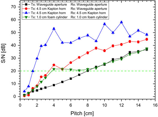
FIGURE 7. S/N in the radio frequency spectrum with LOS induced crosstalk as function of the antenna pitch for different setups [26].
In the absence of any mitigation a minimum pitch of about 8 cm is necessary to achieve a S/N of 20 dB. With one highly directive (17 dBi) Al-Kapton® horn antenna on the transmitting or receiving side, the minimum pitch is reduced to 4 cm, while with Al-Kapton® horn antennas installed on both sides, links can be placed as close as 2 cm next to each other without significant interference effects. Without using any directive antennas crosstalk can be reduced just by absorber shields. This has been tested by equipping all transmitters and receivers with 1 cm long, hollow graphite foam cylinders on top of the waveguide apertures to shield lateral radiation. Then shielded links can be placed as close as 4 cm next to each other.
The Bit Error Rate (BER) measures the performance of a data transmission device. With the setup described above the BER is measured for a data rate of 1.76 Gbps using Minimum Shift Keying (MSK) as modulation scheme. Both links use the same polarization state and the same carrier frequency. Figure 8 shows the BER measured as function of the pitch in different configurations. With horn antennas bit error rates smaller than 10–12 are achieved for all considered pitches.
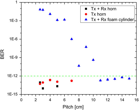
FIGURE 8. Influence of LOS crosstalk on the BER of a wireless data transmission, shown as function of the pitch between two parallel links. Distance between transmitter and receiver is set to 10 cm. Both links are operated at the same carrier frequency [26].
In a real tracking detector 60 GHz radiation can be partially reflected between the silicon detector layers, generating multipath and crosstalk. The silicon detector environment can be simulated by enclosing the volume with aluminium plates (Figure 6). The distance between the links is set to 5, 10 and 15 cm. The measurements relative to all antenna setups with both polarization states (parallel and orthogonal) between the two links are displayed in Figure 9. With directive antennas, stable data transmission at a pitch of 5 cm is possible for all studied configurations. For orthogonal polarization of neighbouring links, a good S/N is obtained for all tested setups even without directive antennas and a distance smaller than 5 cm seems to be possible. The combination of directive antennas and absorbing foam can increase the S/N ratio further. Thus using directive antennas, polarization, absorber materials, alone or in combination allows the operation of 60 GHz links between highly reflective materials even at a small pitch.
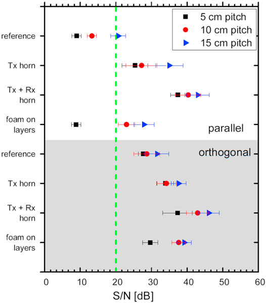
FIGURE 9. S/N for two parallel links operated between two fully reflective aluminium layers at a distance of 10 cm. Results are shown for parallel polarization states (top, white background) and orthogonal polarization states (bottom, grey background) [26].
A transmitter chip with tunable carrier frequency allows the use of frequency channeling. The BER has been measured as a function of the carrier offset when two parallel links are positioned at a pitch of 2.6 cm using the same polarization state. Foam cylinders on top of the waveguide apertures provide a minimum shielding. The carrier frequency offset is varied in steps of 500 MHz. Figure 10 shows that with this setup, using 3 frequency channels in parallel within the full 60 GHz band seems possible. Drawing full benefit from channeling necessitates filters with very sharp cutoff frequencies.
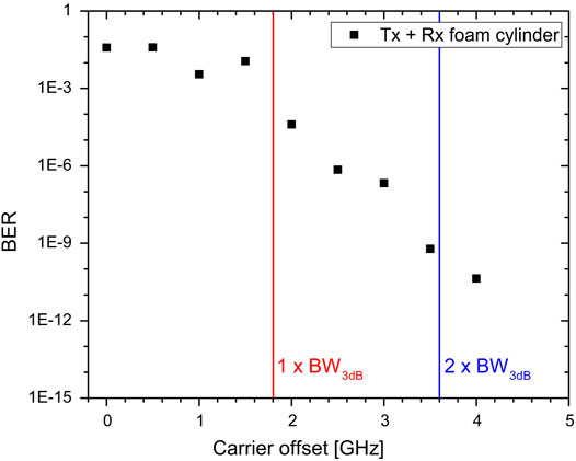
FIGURE 10. Measured BER of two parallel-operated links at a pitch of 2.6 cm as function of the carrier frequency offset. The links are operated with MSK at up to 1.76 Gbps. No directive antennas are used. The 3 dB bandwidth of the Hititte transceivers (1.8 GHz) is indicated as red line, twice the bandwidth as a blue line [26].
An estimate on the possible link density can be derived from above results. Assuming a tracking detector environment with distances of 10 cm between layers and a minimum pitch of 3.5 cm between links., OOK as modulation scheme with a spectral efficiency of ρOOK ≈ 0.5 bps/Hz, and using the full 9 GHz bandwidth per channel yields a data rate of 4.5 Gbps per link, the resulting data rate area density is about 3.7 Tbps/m2. This is a theoretical limit, which cannot be realistically reached experimentally. The estimated experimental data rate density is rather around 1.2 Tbps/m2 [26].
The pickup of noise from 60 GHz communications is a potential worry for the operation of wireless links inside the detector. However, as cut-off frequencies of sensors and readout chips for silicon detectors are typically below a few GHz, no interference between the 60 GHz links and tracking detector modules is expected. To demonstrate this, 60 GHz irradiation tests are performed for different silicon strip and pixel detectors.
Two ATLAS Binary Chip-Next (ABCN) endcap electronics hybrid prototypes for the Phase-2 upgrade of the silicon tracking-detector for the ATLAS experiment are tested using the setup shown on Figure 11. One is a bare electronics hybrid, while the other one is connected to short silicon strip sensors with a strip length of 2.4 cm. Each prototype includes 12 fully functional ABCN readout chips. Noise is measured for each channel of the readout ASICs under wireless irradiation. The hybrid module is irradiated using a 20 dBi horn antenna from an distance of 1 cm resulting in a irradiated power of about −1 dBm. Four different components are irradiated (Figure 11) with carrier frequencies of 57, 60 and 63 GHz: (A) the power converter, (B) and (C) the readout chips, and (D) the bonding wires. The noise level distribution of a reference measurement and a measurement with 60 GHz irradiation are compared in Figure 12 for the electronics hybrid without silicon strips and no significant differences are found in the mean and width of the noise distributions. Similarly no significant noise increase for the second prototype connected to silicon strips is observed. As expected, no influence of the wireless signal on the noise level is found at any carrier frequency.
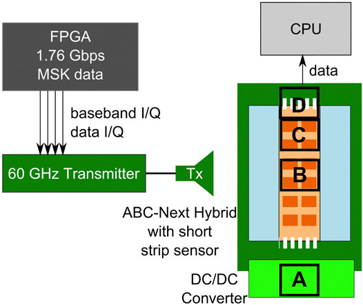
FIGURE 11. Block diagram of the setup used for the irradiation test at Freiburg. A, B, C and D indicate different antenna positions used in the test. The 12 readout chips are illustrated as brown boxes on the orange readout hybrid [26].
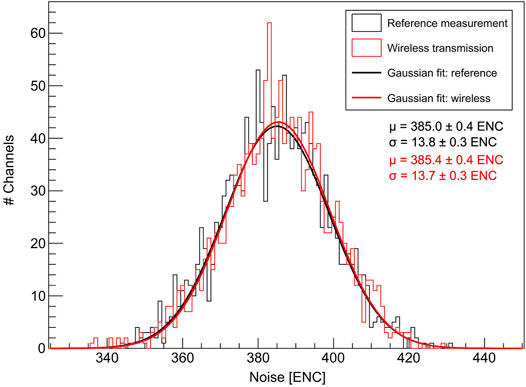
FIGURE 12. Noise distribution of all channels of the 12 ABCN readout chips without strip sensors under irradiation. The reference measurement was performed without 60 GHz irradiation. Mean μ and width σ of the Gaussian fits are given. No significant difference is observed [26].
These results indicate that there should not be any obstacle to wireless data transmission in the 60 GHz band with respect to the operation and performance of current silicon tracking detector sensors [26].
The performance of non-coherent chips described in [2] was measured at 1–5 cm range between transmitter and receiver using low directivity antenna (Figure 13). The transmitter was fed by a SLVS 8b/10b encoded signal from pseudo random binary sequence at 5 Gbps. At the receiver output the binary signal showed less than 75 ps total jitter, less than 35 ps 20–80% rising/falling time and less than 1 ns latency (without the cables). A range of 10 cm can be obtained using 10 dB gain antenna.
A non-coherent transceiver was interfaced with Minimum Ionizing MOnolithic Active pixel Sensors (MIMOSA) from IPHC Strasbourg (Figure 14), which use the epitaxial layer of standard CMOS (TowerJazz High Resistivity 180 nm technology [29]) processes as detecting sensitive volume. The pixel detector board provides 5 μs refreshment rate and generates up to 3 Gbps data rate. Signal integrity tests were carried out with the detector feeding a wireless link. No error was reported at oscilloscope. Different materials were then introduced between the antennas. Signals well passed through the non-metallized area of the thin flex Kapton PCB that embeds chips, but not through low-density carbon foam that holds the detector. These results validate the proposed readout architecture, whose principle is to isolate every detector layer and export data through multiple hops between layers. At longer term, the RF transceiver may be integrated within the detector chip. The antenna could also be part of the chip with good efficiency, assuming the high resistivity substrate of the CMOS backend material. Pixel detectors still need to receive a clock or trigger reference from the network. It could then be worth modifying the 60 GHz transceiver, so that the clock is also transmitted wirelessly from chip to chip on the carrier by harmonic injection locking.
A first irradiation experiment with protons was performed at Åbo Akademi University, Turku, Finland [30]. Figure 15 shows a scheme and a picture of the setup. The radiation hardness of the V-band TRX chip in 65 nm CMOS, acting both in TX and RX modes, was investigated after 17 MeV proton irradiation. TID and fluence used during the experiment were 74 and 42 kGy and 1.4 × 10 14Neq/cm2 and 0.8 × 10¹⁴Neq/cm2 for the RX and the TX, respectively. Transmission performance was measured before, during and after irradiation. The RX experienced higher loss of sensitivity than the TX power loss, accordingly to the respective TID and fluence. However, both the RX and the TX were found operational through over-the-air measurements at 5 Gbps after irradiation. If some transmission errors were observed during the irradiation, the chip recovered error free transmission after irradiation with small gain degradation.
Although the radiation levels expected in the real experiment at HL-LHC or future hadron colliders are much higher, this experiment presents a first investigation of radiation hardness that gives encouraging results despite the fact that the devices were not specifically radiation hardened by either design or process.
A second campaign of irradiation with electrons was carried out at the CLEAR (CERN Linear Electron Accelerator for Research) facility at CERN [31]. The TX and RX were exposed to a TID of 3.14 and 2.70 MGy respectively. The pre- and post-irradiation characterization of the chips revealed a 80 MHz upshift in the centre frequency. An overall link budget degradation of 10 dB was observed, which is a sum of 4 dB reduced TX output power and 6 dB degraded receiver sensitivity. Besides, circuit bandgap (voltage reference) were degraded, which affected the transceivers internal biasings and so the transmitter and receiver gains. Despite the mentioned degradation, the chips were found operational in the post-irradiation characterization. Moreover, margins have been taken in chip design in order to guarantee performance through P,V,T variations and production yield, so that calibration means can restore part of the chip performance. Indeed TX power can be increased by 3dB by changing the settings, while LNA gain can be boosted also to restore the sensitivity. Radiation hardening shall however be considered on C65SPACE (which includes libraries with hardened cells, tested up to 0.3 Mrad dose but could handle higher radiations) or more advanced SOI technology for the highest radiation levels expected at future colliders such as HL-LHC or FCC-hh.
At long term, the integration of wireless technologies in tracking detector would certainly require the design of a dedicated radiation hardened mmw transceiver IP, to be integrated either as a companion chip or within silicon trackers. For this purpose the ST C65SPACE radiation hardened ASIC technology or 45 nm Partially Depleted SOI technologies seem good candidates. The latter would allow the integration of antenna directly on the High Resistivity substrate of its back-end. For a better and versatile interfacing, the transceiver IP could also contain serializer/deserializer. External antennas or focusing lenses should be envisaged with the objectives of extending the range and ease crosstalk management. The crosstalk can be further improved by alternating antennas radiating in vertical and horizontal polarization for better isolation. The antenna should radiate a vertical beam (normal to the PCB plane) in order to fit easily in the detector.
At shorter term is envisaged the integration of the available non coherent mmw transceivers BGA with external antennas, as System In Package or System On Board. The antenna shall provide a narrow beam broadside for dense wireless links. As a proof of concept, a three (or four) layer silicon detector will be build3, as shown on Figure 3. This mock-up of a central tracker will be equipped with the transceiver chip in BGA package. This will allow to study the added noise and data transmission quality (impact on eye diagram, Jitter, Bit Error Rate) over the different layers and get the antenna specifications: gain, polarization, bandwidth and radiation robustness. Then we will integrate the detectors to the setup to check the readout capabilities while using multi-hop wireless link. Eventually a multilink scenario will be considered to check if the isolation between channels is sufficient for the considered application. This would bring us closer to the full scale implementation and would help specify and integrate the future wireless systems in detectors at future colliders.
The recent advances in mmw technologies allows low latencies, high data rates and low power wireless data transmission at short range. The association of non-coherent RF architecture and directive antennas are particularly relevant for the considered innermost part of the readout network, based on multi-hop transmission. Early feasibility tests with prototypes and commercial products have demonstrated that crosstalk is not an issue for high density of links and that no pickup noise is to be expected. The projected theoretical limit with current technology is 3.7 Tbps/m2 and <10 pJ/bit. Although the commercial products were not designed nor manufactured as radiation hard components, they showed good behaviour under irradiation with protons and electrons. They could be easily hardened to be able to sustain radiation levels expected at future hadron colliders. There is no show-stopper to the early deployment and proof of concept using hardened RFICs and associated electronics in HEP experiments. The mmw technological roadmap shows soaring data rates using higher frequency bands above 100 GHz, challenging optical links for data aggregation and routing at short to medium range.
Well-chosen detector technology and geometry, combined with flexible wireless techniques might help in minimizing dead material by reducing the amount of cables and connectors. The absence of constrain to mechanical structures allows radial readout following the event topology that would be optimal for a fast trigger decision and would enhance on-detector intelligence, which could also open up new possibilities of communication between chips.
Technologies should be mature enough to be envisaged as a part of the readout network of future detectors at future colliders.
All authors listed have made a substantial, direct, and intellectual contribution to the work and approved it for publication.
The authors declare that the research was conducted in the absence of any commercial or financial relationships that could be construed as a potential conflict of interest.
All claims expressed in this article are solely those of the authors and do not necessarily represent those of their affiliated organizations, or those of the publisher, the editors and the reviewers. Any product that may be evaluated in this article, or claim that may be made by its manufacturer, is not guaranteed or endorsed by the publisher.
The present document is based on the work of the whole WADAPT consortium4, which has been partly presented at the 40th International Conference on High Energy physics—ICHEP2020 [2]. The authors are grateful to their colleagues of the Heidelberg University, Sebastian Dittmeier, André Schöning, Hans Kristian Soltveit, Dirk Wiedner, for giving them the permission to use in extenso large parts of their publication [26] for the sake of the completeness of this review. Special thanks are due to Sebastian Dittmeier for the tests of the Hittite transceiver, to Imran Aziz for the irradiation tests, to Frederic Lagrange from STMicroelectronics for providing equipment and support, to our colleagues5 of the Institut Pluridisciplinaire Hubert Curien, Strasbourg, France for the tests of connectivity to MIMOSA sensors as well as to Åbo Akademi University, Finland for use of their irradiation facility. Warm thanks go to Hans Kristian Soltveit for the careful reading of this document.
1The latest description of the pixel detector layout, including the number of staves per barrel and endcap layer, the number of sensors per stave and the estimated data rates per chip can be found in [6].
2Here the signal to noise ratio is defined as the average received signal over the bandwidth, and the noise is defined as the average noise or interference power over the bandwidth.
3This project is supported by AIDAinnova.
4R. Brenner, D. Dancila, C. Dehos, P. De Lurgio, Z. Djurcic, G. Drake, J.L. Gonzalez Jiménez, L. Gustafsson, D.W. Kim, E. Locci, U. Pfeiffer, D. Röhrich, D. Rydberg, A. Schöning, A. Siligaris, H.K. Soltveit, K. Ullaland, P. Vincent, P.R. Vasquez, D. Wiedner, S. Yang.
5J. Baudot, G. Claus, M. Goffe.
1. Brenner R, Ceuterickx S, Dehos C, De Lurgio P, Djurcic Z, Drake G, et al. Development of Wireless Techniques in Data and Power Transmission Application for Particle-Physics Detectors. (2017) CERN-LHCC-2017-002; LHCC-I-028 Available from: https://cds.cern.ch/record/2243480?ln=fr.
2. Dehos C, Locci E, Brenner R, Dancila D, de Lurgio P, Djurcic Z, et al. Wireless Allowing Data and Power Transfer. In: Proceesing of the 40th International Conference on High Energy physics - ICHEP (2020) ; Jul 2020; Prague, Czech Republic. p. 832.
3.The ATLAS Collaboration. The ATLAS experiment at the CERN Large Hadron Collider. J Instrum (2008) 3:S08003. doi:10.1088/1748-0221/3/08/S08003
4.The CMS Collaboration. The CMS experiment at the CERN Large Hadron Collider. J Instrum (2008) 3:S08004. doi:10.1088/1748-0221/3/08/S08004
5. Béjar Alonso I, Brüning O, Fessia P, Lamont M, Rossi L, Tavian L, et al. High-Luminosity Large Hadron Collider (HL-LHC): Technical Design Report. In: CERN Yellow Reports: Monographs (2020). p. 378. CERN-2020-010. doi:10.23731/CYRM-2020-0010
6.ATLAS PUB Note. Expected Size and Read-Out Rate of the Data of the ATLAS ITk Pixel Detector (2022). Available from: https://cds.cern.ch/record/2800852/files/ATL-ITK-PUB-2022-001.pdf.
7. Sguazzoni G. The CMS Pixel Detector for the High Luminosity LHC. Nucl.Instrum.Meth.A (2019) 958:162089. doi:10.1016/j.nima.2019.04.043
8. Affolder A, Allongue B, Blanchot G, Faccio F, Fuentes C, Greenall A, et al. DC-DC Converters with Reduced Mass for Trackers at the HL-LHC. J Inst (2011) 6:C11035. doi:10.1088/1748-0221/6/11/c11035
9. Rappaport TS, Murdock JN, Gutierrez F. State of the Art in 60-GHz Integrated Circuits and Systems for Wireless Communications. Proc IEEE (2011) 99(No. 8):1390–436. doi:10.1109/jproc.2011.2143650
10. Siligaris A, Hamada Y, Mounet C, Raynaud C, Martineau B, Deparis N, et al. A 60 GHz Power Amplifier with 14.5 dBm Saturation Power and 25% Peak PAE in CMOS 65 Nm SOI. IEEE J Solid-State Circuits (Jssc) (2010) 45(7):1286–94. doi:10.1109/jssc.2010.2049456
11. Siligaris A, Richard O, Martineau B, Mounet C, Chaix F, Ferragut R, et al. A 65 Nm CMOS Fully Integrated Transceiver Module for 60 GHz Wireless HD Applications. In: Proceeding of the International Solid-State Circuits Conference (ISSCC); San Francisco (2011). p. 20–4.
12. Siligaris A, Richard O, Martineau B, Mounet C, Chaix F, Ferragut R, et al. A 65-nm CMOS Fully Integrated Transceiver Module for 60-GHz Wireless HD Applications. IEEE J Solid-State Circuits, 46 (2011). p. 3005–17. doi:10.1109/jssc.2011.2166662
13. Kaouach H, Dussopt L, Lanteri J, Koleck T, Sauleau R. Wideband Low-Loss Linear and Circular Polarization Transmit-Arrays in V-Band. IEEE Trans Antennae Propagation (2011) 59:2513–23. doi:10.1109/tap.2011.2152331
14. Pfeiffer UR, Goren D. A 20 dBm Fully-Integrated 60 GHz SiGe Power Amplifier with Automatic Level Control. IEEE J Solid-state Circuits (2007) 42(7):1455–63. doi:10.1109/jssc.2007.899116
15. Reynolds SK, Floyd BA, Pfeiffer UR, Beukema T, Grzyb J, Haymes C, et al. A Silicon 60-GHz Receiver and Transmitter Chipset for Broadband Communications. IEEE J Solid-state Circuits (2006) 41:2820–31. doi:10.1109/jssc.2006.884820
16. Diet A, Villegas M, Baudoin G, Robert F. Radio-communications Architectures. In: A Bazzi, editor. Radio Communications. Sciyo: Intech (2010). p. 1–35. ffhal-00553229f.
17. Siligaris A, Deparis N, Pilard R, Gloria D, Loyez C, Rolland N, et al. A 60 GHz UWB Impulse Radio Transmitter with Integrated Antenna in CMOS65nm SOI Technology. In: Proceeding of the 2011 IEEE 11th Topical Meeting on Silicon Monolithic Integrated Circuits in RF Systems; Jan. 2011; Phoenix, AZ. IEEE (2011). p. 153–6. doi:10.1109/SIRF.2011.5719303
18. Dussopt L, Lamy Y, Joblot S, Lanteri J, Salti H, Bar P, et al. Silicon Interposer with Integrated Antenna Array for Millimeter-Wave Short-Range Communications. In: Proceeding of the 2012 IEEE/MTT-S International Microwave Symposium Digest; June 2012; Montreal QC. IEEE (2012). p. 1–3. doi:10.1109/MWSYM.2012.6259424
19. Soltveit HK. Multi-Gigabit Wireless Data Transfer for High EnergyPhysics Applications. In: Proceedings of The European Physical Society Conference on High Energy Physics — PoS(EPS-HEP2017); October 2017 (2017). doi:10.22323/1.314.0520
20. Gonzalez-Jimenez JL, Dehos C, Cassiau N, Siligaris A, Clemente A, D’Errico R, et al. Channel-bonding CMOS Transceiver for 100 Gbps Wireless point-to-point Links. EURASIP J Wireless Commun Networking, 2020 (2020). p. 117. doi:10.1186/s13638-020-01741-1
21. Manzillo FF, Luis Gonzalez-Jimenez J, Clemente A, Siligaris A, Blampey B, Dehos C. Low-cost, High-Gain Antenna Module Integrating a CMOS Frequency Multiplier Driver for Communications at D-Band. In: Proceedings of The 2019 IEEE Radio Frequency Integrated Circuits Symposium (RFIC); June 2019; Boston, MA, USA. IEEE (2019). p. 19–22. doi:10.1109/RFIC.2019.8701772
22. Voineau F, Dehos C, Martineau B, Sie M, Perchicot M, Nguyen NH, et al. A 12 Gb/s 64QAM and OFDM Compatible Millimeter-Wave Communication Link Using a Novel Plastic Waveguide Design. In: Proceedings of The 2018 IEEE Radio and Wireless Symposium (RWS); Jan 2018; Anaheim, CA. IEEE (2018). p. 250–2. doi:10.1109/RWS.2018.8305001
23. Muñoz Sánchez F. Module and Electronics Developments for the ATLAS ITk Pixel System. In: Proceedings of The 19th iWoRiD; Krakow, Poland (2017).
24. Brenner R, Cheng S. Multigigabit Wireless Transfer of Trigger Data through Millimetre Wave Technology. J Instrumentation (2010) 5:c07002. doi:10.1088/1748-0221/5/07/c07002
25. Dehos C, González JL, De Domenico A, Kténas D, Dussopt L. Millimeter-wave Access and Backhauling: the Solution to the Exponential Data Traffic Increase in 5G mobile Communications Systems? IEEE Commun Mag (2014) 52(9):88–95. doi:10.1109/MCOM.2014.6894457
26. Dittmeier S, Schöning A, Soltveit HK, Wiedner D. Feasibility Studies for a Wireless 60 GHz Tracking Detector Readout. Nucl.Instrum.Meth. (2016) A830:417–26. doi:10.1016/j.nima.2016.06.016
27.Analog Devices. Millimeterwave Transmitter 57 - 64 GHz. Available from: https://1224 www.analog.com/media/en/technical-documentation/data-sheets/hmc6000.pdf (Accessed 2012).
28.Wireless-Connectivity. Wireless-Connectivity. Available from: https://www.st.com/en/wireless-connectivity/st60a2g0.html (Accessed 2022).
29. Pernegger H. Monolithic Pixel Development in TowerJazz 180 Nm CMOS for the Outer Pixel Layers in the ATLAS experiment. Nucl Instr Methods Phys Res Section A: Acc Spectrometers, Detectors Associated Equipment (2018) 924:92–8. doi:10.1016/j.nima.2018.07.043
30. Aziz I, Dancila D, Dittmeier S, Siligaris A, Dehos C, De Lurgio PM, et al. Effects of Proton Irradiation on 60 GHz CMOS Transceiver Chip for Multi-Gbps Communication in High-Energy Physics Experiments. J Eng (2019) 8:5391. doi:10.1049/joe.2018.5402
Keywords: wireless, data transfer, WADAPT, vertex detector, collider
Citation: Brenner R, Dehos C and Locci E (2022) Multi Gigabit Wireless Data Transfer in Detectors at Future Colliders. Front. Phys. 10:872691. doi: 10.3389/fphy.2022.872691
Received: 09 February 2022; Accepted: 21 April 2022;
Published: 16 June 2022.
Edited by:
Petra Merkel, Fermi National Accelerator Laboratory (DOE), United StatesReviewed by:
David Christian, Fermi National Accelerator Laboratory (DOE), United StatesCopyright © 2022 Brenner, Dehos and Locci. This is an open-access article distributed under the terms of the Creative Commons Attribution License (CC BY). The use, distribution or reproduction in other forums is permitted, provided the original author(s) and the copyright owner(s) are credited and that the original publication in this journal is cited, in accordance with accepted academic practice. No use, distribution or reproduction is permitted which does not comply with these terms.
*Correspondence: R. Brenner, UmljaGFyZC5CcmVubmVyQGNlcm4uY2g=
Disclaimer: All claims expressed in this article are solely those of the authors and do not necessarily represent those of their affiliated organizations, or those of the publisher, the editors and the reviewers. Any product that may be evaluated in this article or claim that may be made by its manufacturer is not guaranteed or endorsed by the publisher.
Research integrity at Frontiers

Learn more about the work of our research integrity team to safeguard the quality of each article we publish.