
94% of researchers rate our articles as excellent or good
Learn more about the work of our research integrity team to safeguard the quality of each article we publish.
Find out more
REVIEW article
Front. Phys. , 20 November 2020
Sec. Radiation Detectors and Imaging
Volume 8 - 2020 | https://doi.org/10.3389/fphy.2020.593076
This article is part of the Research Topic Electronics and Signal Processing View all 20 articles
Microwave impedance microscope (MIM) is a near-field microwave technology which has low emission energy and can detect samples without any damages. It has numerous advantages, which can appreciably suppress the common-mode signal as the sensing probe separates from the excitation electrode, and it is an effective device to represent electrical properties with high spatial resolution. This article reviews the major theories of MIM in detail which involve basic principles and instrument configuration. Besides, this paper summarizes the improvement of MIM properties, and its cutting-edge applications in quantitative measurements of nanoscale permittivity and conductivity, capacitance variation, and electronic inhomogeneity. The relevant implementations in recent literature and prospects of MIM based on the current requirements are discussed. Limitations and advantages of MIM are also highlighted and surveyed to raise awareness for more research into the existing near-field microwave microscopy. This review on the ongoing progress and future perspectives of MIM technology aims to provide a reference for the electronic and microwave measurement community.
The past decade has witnessed efforts in the field of microwave to develop a near-field scanning microwave microscope (NSMM) as a scientifically powerful instrument with rapid development [1–9]. Early implementations of the microscope either used a small aperture at microwave cavities [2, 4] or a needle-shape probe coupled to a microwave resonator [5, 8–11]. Due to the hardship in tip-sample distance control, these approaches are intrinsically susceptible to tip damage and difficult in nanoscale quantitative measurement applications [9, 12]. The microwave impedance microscope (MIM) can control tight distance perfectly and solve the crucial probe-sample gap control issue in the nanometer range NSMM. Moreover, it shows great advantages in reducing the loss in doped silicon traces while ensuring large power gain and high sensitivity because it employs metal lines for the electrodes and cancels background signal before amplification. In addition, the MIM can significantly suppress the common-mode signal since the inductive probe is separated from the excitation electrode. Compared to atomic force microscopy (AFM) and scanning tunneling microscopy (STM), the long-range electrostatic force involved in scanning MIM reduces the stringent requirements for proximal probes, enabling high-speed, non-contact, and non-destructive measurements [13–16]. Due to the aforementioned advantages, the MIM achieves near-field measurements at nanoscale and has great potential in future application of high-resolution microwave images generation.
In this review, we present a comprehensive study of development and recent progress in MIM. This review focuses on technique improvements and applications and covers MIM limitations and advantages, as well as the opportunities for further research into the subject of near-field measurement. The rest of this paper is organized as follows. Basic Design and Improvement of Scanning Microwave Impedance Microscopy gives a brief history and an overview of the structure of MIM and discusses the fabrication process and improvement of MIM. Cutting-Edge Application of Microwave Impedance Microscope treats various cutting-edge applications. Conclusion presents the conclusions and discussion.
The employment of microwave frequency band has many advantages, such as strong penetration, the ability to detect the internal information of the sample, and the common polarization of short relaxation time by the frequency influence. The near-field microwave microscope works in the same principle in several generations. The resonator resonates in the λ/4 coaxial resonator through the coupling loop, then the resonant signal acts on the sample after the needlepoint conduction. The microwave reflection of the sample absorbed by the resonator will interact with the microwave resonance. It causes resonance frequency change. The reflected microwave decays quickly and is much smaller than the microwave output signal, so the perturbation equation can be used to analyze it [17–19]. Scanning microwave microscopy (SMM) is a powerful tool for the investigation of various properties, including conductivity, permittivity, and impedance at the nanoscale. Different kinds of resonant SMMs with excessive sensitivity and spatial resolution have been demonstrated [5–9]. Despite the great progress in SMMs, various barriers exist in current designs [14, 20]. A case in point is the large common-mode signal, which results in loud noise. Slow operation and low bandwidth dampen the special effect of long-range force involved in a microwave microscope. Scanning microwave impedance microscopy (MIM) is a species of SMM [21–26]. MIM solves this problem successfully. Unlike traditional SMMs, MIM determines the electrical properties through the analysis of the phase and amplitude of the reflected wave instead of through frequency drift and quality factor change. The preponderance of this technique is that it shields the external signal and reduces the common-mode signal. MIM detects dielectric responses at a much wider frequency range (GHz). MIM demonstrates the capacity to acquire high-resolution microwave images of buried structures, as well as nanoparticles, nanowires, and biological samples.
In Ref. 27, a handy and clear explanation of MIM system characteristics was introduced. As shown in Figure 1, system characterization involved tip-sample interaction, impedance matching, and microwave circuitry. The outstanding point of MIM is that the sensor probe is separated from the excitation electrode while maintaining high sensitivity and spatial resolution. The schematic construction of MIM was shown in Figure 2, in which the traditional tip is replaced with a standard AFM tip assembly and two transmission lines are included, one for excitation and the other for sensing. A two-layer implementation like this improves the system’s common-mode rejection ratio and reduces the noise level significantly. With appropriate design, the detector can be “orthogonal”. Then the signal is minimized without a sample. A high throughput near-field scanning microwave microscope can be implemented. Besides the sharp sensing electrode, a second electrode surrounding the tip is also present on the cantilever to significantly suppress the common-mode signal.
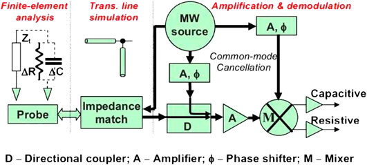
FIGURE 1. Schematic diagram of MIM. Reproduced with permission from Rev. Sci. Instrum. 79, 6 (2008). Copyright 2008 American Institute of Physics.
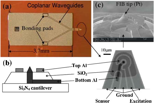
FIGURE 2. The schematic construction of MIM. (A) Microfabricated microwave probe with two aluminum electrodes and the ground plane patterned on the Si nitride cantilever. (B) Schematic drawing of the layer structure near the probe end. (C) SEM image near the probe end [27]. Reproduced with permission from Rev. Sci. Instrum. 78, 6 (2007). Copyright 2007 American Institute of Physics.
In Ref. 28, the lumped element circuit description is related to the representative probe, with three impedances Ze, Zt, and Zet as illustrated in Figure 3. Since there is a large mismatch between Zt (Ze) and the transmission line impedance Z0(50 Ω), the microwave power cannot be transmitted to the probe, and detecting a small microwave impedance variation is infeasible if the microwave power is directly connected to the feeder. In order to improve the transmission of microwave power, it is important to achieve impedance matching. The tip of the MIM is first connected to a portion at the end of a λ/4 section of a transmission line to form a resonator. As shown in Figure 3, the resonator is then critically coupled to the feed line by a parallel open-end tuning stub. An almost perfect match is easily obtained with this adjustable stub [29].

FIGURE 3. Impedance matching section. A λ/4 cable and a tuning stub (inside the dashed boxes) form the interface between the probe and the 50 Ω feed lines [28]. Reproduced with permission from Rev. Sci. Instrum. 79, 6 (2008). Copyright 2008 American Institute of Physics.

FIGURE 4. Depiction of the experimental set up for sMIM. [30] Reproduced with permission from Appl. Nanosci. 1, 1 (2011). Copyright 2011 Springer Nature.
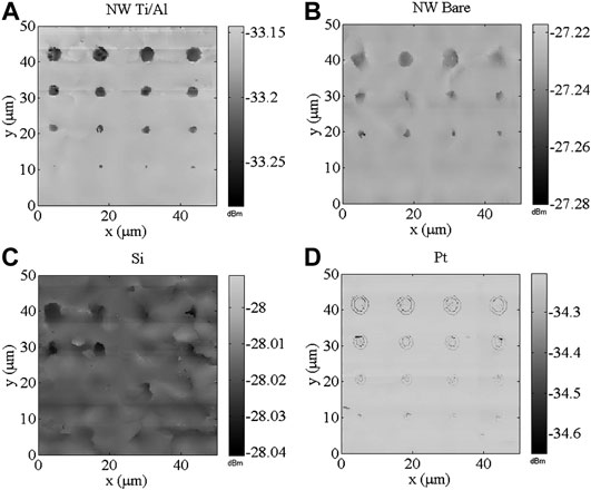
FIGURE 5. S11 image with four different probes indicates a minimum sensitivity. [40] (A) Scan results for the Ti/Al NW probe over DUT showing the change in the amplitude of the microwave reflection coefficient S11. All micro-capacitors are present in the image, indicating sensitivity to at least 0.7 fF. (B) S11 image with a bare NW probe indicates a minimum sensitivity of 3 fF. (C) S11 image with Si probe indicates a minimum sensitivity of 6 fF. (D) S11 image with Pt probe indicates a minimum sensitivity of 0.7 fF. All scans are plotted with different Z-axis color scales for clarity. All micro-capacitors are present in the image, indicating sensitivity to at least 0.7 fF [40]. Reproduced with permission from Appl. Phys. Lett. 104, 2 (2014). Copyright 2014 American Institute of Physics.
In Ref. 30, the microwave is conducted into the tip through a directional coupler. Then it gets into the directional coupler after the surface reflection, and a cancellation signal is inputted to suppress the background reflected signal at the same time. Reflection microwave signals and cancellation signals are amplified and demodulated to the quadrature mixer. Finally, the reflected signal is composed of in-phase and out-of-phase components [28, 29]. It contains data about the local permittivity (capacitance) and conductivity (resistance) of the sample. But there are still some problems. The tip electrode is the most sensitive to local electrical performance, while the ring electrodes to topography. Therefore, combining the signals from the two electrodes may eliminate the convolution of electrical and topographical information.
In recent years, MIM has been developed to characterize the electrical properties of samples such as permittivity and conductivity. Accordingly, the need for MIM is increased. Many recent articles discuss the improvement of MIM in sensitivity, resolution and wideband. Meanwhile, tip wearing and sample dragging have become an increasingly serious issue in near-field microwave measurement. Many researchers have been able to make probes on a large scale by improving the manufacturing process [31]. Table 1 compares and summarizes different techniques and methodologies for the improvement of MIM.
In Ref. 32, a compact mode microwave impedance imaging based on an atomic force microscope platform was proposed. Tap mode microwave imaging was also superior to contact mode because thermal drift and other electron drift observed in contact mode can be completely eliminated and absolute measurements of dielectric properties can be made. Because the actual tip-sample interaction is modulated at the tapping frequency, slowly varying temperatures and other electronic drifts that occur over a longer time frame do not contaminate the microwave image [33–35]. Since the cantilever probe oscillates at its resonant frequency, it only intermittently contacts the surface of the sample. Tip wear and sample drag are greatly reduced. It was also shown that the tap mode MIM can be executed on the actual Nanodevices.
In Ref. 36, the authors reported the design and fabrication of a piezoresistive cantilever with a low-impedance conduction line to our electrically-shielded tip. Their new design exhibits a vertical displacement resolution of 3.5 nm in a measurement bandwidth from 1 Hz to 10 kHz. The probes provide topography feedback with nanometer vertical resolution for samples or setups where laser detection is not feasible or desirable. Furthermore, the low parasitic impedance of the tip enables MIM measurements. Although the capacitance and resistance of the tip are not as low as previously reported probes, the measured impedance suggests MIM measurements can be obtained in a self-sensing mode, though with decreased MIM sensitivity and thus contrast [37–39]. The self-sensing cantilever allows topography feedback where the laser beam bounce technique is not available or hard to implement. This probe will enable coupled topography scans with MIM images.
In Ref. 40, a novel fabrication in a GaN nanowire probe for near-field scanning microwave microscopy was suggested and investigated, with improved sensitivity and reduced uncertainty achieved which can measure capacitance values down to as small as 0.7 fF while simultaneously recording 10 nm height changes. The changes of the Mean measurement parameter (S11) sensitivity that the nanowire probe is coated a Ti/Al layer and across the device under test (DUT) micro capacitors were much greater than a commercial Pt NSMM probe [41–45]. The measurement uncertainty was significantly reduced. It is important to improve wear resistance during contact-mode scanning. The high-intensitive of the defect-free nanowire improved measurement repeatability and alleviated the need to re-calibrate the system frequently because it keeps the tip radius constant between the scans.
In Ref. 46, the authors reported a new type batch-processed low impedance, well-shielded and sharp tips piezoresistive cantilever probes for simultaneously topographical and electrical scanning probe microscopy. The integration of a piezo resistor on MIM probes is a challenging task [47–49]. The small resistance and capacitance, as well as the shielded structure, ensure great electrical performance. High quality piezo resistive topography and MIM images are simultaneously obtained with the fabricated probes [50–52]. These novel piezoresistive probes remarkably broaden MIM applications in scientific and engineering research of new materials and electronic devices by operating photosensitive samples with an integrated feedback mechanism at low temperatures. The probes show good piezoresistive topographic and MIM capability at both room and cryogenic temperatures.
In Ref. 53, the main idea was to integrate a scanning microwave microscope into a scanning electron microscope and a focused ion beam (SEM/FIB) instrument for nanoscale imaging, characterization, and manipulation. Scanning electronics and microwave microscopy operated in an open-source automation software environment [54]. The automated operation of nanoobjects goes a step further with the development of hybrid open-source microscope tools. This scanning microwave microscope can image the terrain, measure electromagnetic performance at microwave frequencies, and manipulate the “sample under test.”
In Ref. 55, a simple and novel silicon donor nanostructure design for scanning tunneling microscopy (STM) mode was introduced to quantify the resolution limit of sMIM. The doping pattern is buried under a protective silicon cap by a 10 nm highly conductive silicon line and imaged with sMIM, which is an ideal test for the resolution and sensitivity of sMIM technology because it is made in nm resolution and can reduce the complexity caused by terrain convolution [56–58]. sMIM has been identified as an excellent platform for studying buried donor structures, opening up a field of research with further advantages of this technology, such as monotonic signal response. Looking ahead, sMIM is an ideal technique for identifying buried-pattern devices and may allow for quantified post-processing characterization of donor structures, which may be an important tool for studying atomic-level transistors and the latest quantum computing solutions.
In Ref. 59, the format and overall performance of a fully integrated CMOS-MEMS SMM were described particularly. A measuring unit has been developed, constructed, and applied to enhance the signal to noise ratio and maximize the sensitivity of the CMOS-MEMS SMM system. The block diagram of the complete SMM system includes the tip of the sample being tested, the SMM device fabricated using CMOS-MEMS technology, the matching network, and the measurement circuit [60]. In this situation, an increase in sensitivity means that for a given tip-sample impedance change, the change in system output (Vout or S11 in Figure 6) will be maximized. These experiments confirmed the workable of SMM to reveal characteristics not detected using AFM. These analyses are carried out on the new CMOS-MEMS SMM system described in this paper to assist designers to enhance the sensitivity of traditional SMM systems. The analysis presented in this article applies not only to CMOS-MEMS SMMs but to any kind of SMM.
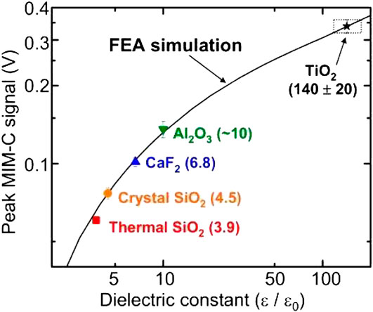
FIGURE 7. Peak MIM-C signal in tip-sample approaching as a function of the relative dielectric constant [61]. Reproduced with permission from Appl. Phys. Lett. 93, 12 (2008). Copyright 2008 American Institute of Physics.
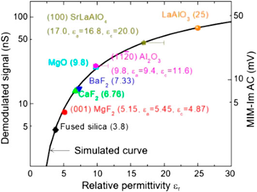
FIGURE 8. Demodulated tip-sample admittance and the corresponding MIM-Im AC signals as a function of the relative permittivity [69]. Reproduced with permission from Rev. Sci. Instrum. 89, 4 (2018). Copyright 2018 American Institute of Physics.
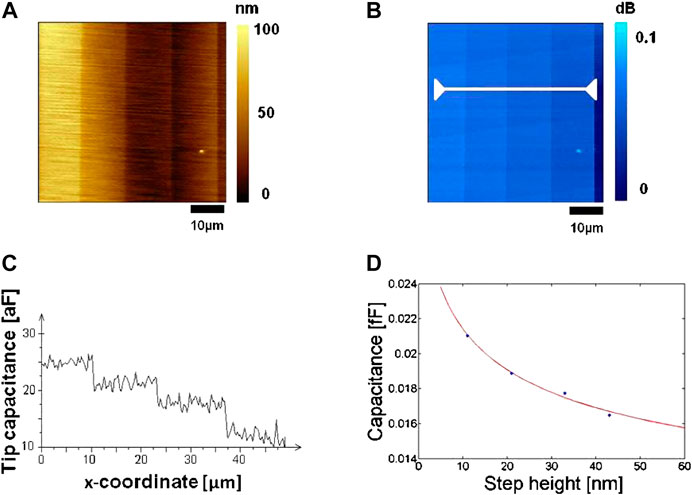
FIGURE 9. AFM-tip/sample capacitance and effective tip radius. [70] (A) Topographical image of the bare 10 nm stepped dielectric staircase structure. (B) Corresponding PNA amplitude image with the different steps resolved (0 dB corresponds to the bare silicon surface, as seen at the far-right edge of the image). (C) The PNA amplitudes were converted to capacitances and plotted concerning the x-coordinate of the white line in (B). (D) For each dielectric step, the capacitance was determined using an area analysis and subsequent averaging of the PNA amplitude [70]. Reproduced with permission from Rev. Sci. Instrum. 81, 11 (2010). Copyright 2010 American Institute of Physics.
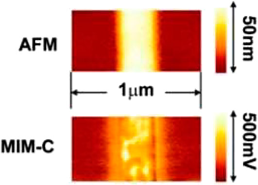
FIGURE 10. Simultaneously taken topography and MIM-C images of an In2Se3 nanoribbon. [72] Reproduced with permission from Nano Lett. 9, 3 (2009). Copyright 2009 American Chemical Society.
sMIM is a quantitative near-field tool [27, 28] that operates at a high-frequency ∼ GHz range [28]. It can detect the electrical properties of various samples and implement microwave detection technology at a macro/nano scale, showing broad application prospects. MIM has made rapid progress. With the passing of the years, many people have participated in the research of MIM application, and push the frontiers of MIM further. MIM technology does not have limitations on the dimensions of the sample as well as on its properties. It can be widely used in semiconductors, insulators, metals, magnetic materials, chemical molecules, and biological cells. In terms of property measurement, it can measure the basic electrical properties such as dielectric constant, conductance, capacitance variation, and electronic inhomogeneity. Recent applications of SMM are summarized in this section.
In Ref. 61, the dielectric constant of materials including high-k insulators can be quantitatively measured and the author measured the approximate curve of an oscillating tip toward bulk dielectric samples using the MIM. Unlike coplanar probes with poor shielding capabilities, which sense a sample distance of tens of microns, the shielding of the wire eliminates spurious signals from the cantilever body and enables quantitative analysis of tip-sample interactions. The approximation curve of the MIM-C channel output can be accurately described by lumped element FEA simulation using standard locking techniques. The peak signal near the curve is a measure of the dielectric constant of the sample and can be used to explore unknown bulk materials [61]. permit by using a large number of dielectrics and permittivity of unknown materials.
In Ref. 62, the authors presented a rigorous modeling of nanosized SMM probes and their electrodynamic interaction with material samples at microwave frequencies [62]. They concluded that the SMM had the potential for use as a broadband dielectric spectroscopy operating at higher frequencies up to THz [63, 64]. The numerical simulation is carried out by the finite element method (FEM). They pointed out that the quasi-static model was accurate in calculating the tip sampling capacitance., and with the increase of frequency, the accuracy of loss calculation decreased [65, 66]. Their simulations show that the SMMs operating at higher frequency provides greater sensitivity on the evaluation of dielectric loss.
In Ref. 67, the authors demonstrated the MIM experiments on a static random-access memory (SRAM) sample to resolve the local conductivity distribution. They showed the microwave imaging on the staircase and SRAM samples in the linear impedance. While the conventional SCM images match the nominal device structure, the MIM images display certain unexpected features of the nominal doping maps, which originate from a thin layer of the dopant ions that go through protective layers during the ion-implantation processes. Real-space mapping of doping concentration in semiconductor devices is of great importance for the microelectronic industry. Their technique can measure the surface impedance by MIM and carry types by SCM. With these capabilities, our technique clearly shows great potentials for applications in the semiconductor industry.
In Ref. 68, the authors created a quantification scheme extracting sample conductivity and permittivity from admittance with only the use of the capacitive calibration die provided by the instrument using simulations and MIM measurements. The prediction was verified with a sample of polytetrafluoroethylene (PTFE). They have provided with finite element simulations the full tip-sample behavior as a function of both permittivity and conductivity. They furthermore demonstrated a method for extracting values of permittivity from the contrast map under certain constraints for the conductivity. Here they supply the full behavior for multiple values of both parameters. MIM is a valuable technique that can image admittance contrast with minimal sample preparation.
In Ref. 69, the authors reported a method for the quantitative measurement of nanoscale dielectric constant and conductivity using a tuning-fork (TF) based MIM. A tuning fork (TF) based MIM with an etched metal tip provides an excellent solution to tip degradation problems. They further developed TF-MIM by using drive amplitude modulation (DAM) mode, which provides satisfactory stability for samples with rough surfaces. The demodulated MIM AC signal was simulated by combining the finite element analysis (FEA) of the leading sample admittance with the Fourier transform of the real-time signal. The simulation results agree well with the experimental data on bulk media and working nanometer devices. This work shows that TF-MIM is an effective tool for quantitative nanoscale imaging of electrical properties in functional materials. Their work provides a method to perform quantitative near-field microwave imaging, where absolute signal levels can be easily construed as local permittivity and conductivity [69].
In Ref. 70, this paper proposes a calibration method that can be widely applied to SMM based on the study of the quantitative dimension of dielectric constants of thin films using SMM. And calibration procedures for nanoscale capacitance measurements permit quantitative evaluation of material and device overall performance in SMM measurements. Customized standard samples, coupled with end-to-end interaction modeling and thorough PNA data processing, make it possible to calibrate SMM parameters, including calibration capacitance and effective probe size. This quantitative information is important to understand the response and conduct of nanoscale systems, in particular when equipment performance must be evaluated over its expected operating frequency range. In order to determine the absolute capacitance value by the PNA reflection amplitude, a calibration pattern of quite a number sizes of conductive gold pads on the SiO2 step shape used to be used.
In Ref. 71, the authors proposed a general method for calculating the change in capacitance of a tip-sample in a near-field scanning microwave microscope. This method can accurately calculate the change in capacitance due to uneven perturbations in insulated or conductive samples, which has been verified by finite element analysis of commercial software and experimental data from MIM. Furthermore, the method presented in this paper also provides a rigorous framework to solve the inverse problem, with great potential to increase the resolution by deconvolution. This method can be applied directly to scanning microscopes and saves a lot of time and memory. The frame is suitable for a wide range of models. Regardless of tip shape, sample type, and disturbing material, the results are very accurate and can be applied to any tip shape, thick film, and variations due to uneven disturbances.
In Ref. 72, the authors reported the observation of electronic inhomogeneity in indium selenide (In2Se3) nanoribbons by near-field scanning MIM. Microwave probes compatible with atomic force microscopy enable quantitative sub-surface electronics research in a non-invasive manner. The large signal with opposite signs recorded by the MIM most vividly displays the phase change memory function of the In2Se3 devices. It is possible to further implement the MIM as a spatially-resolved readout instrument for memories with great resistivity changes [72]. MIM cannot detect small topographic changes with phases changes, but can directly measure local electronic properties and is more sensitive to operations [73–76]. The author demonstrates that the MIM can provide spatially resolved information when In2Se3 nano-devices are phase-switched by voltage pulses [72].
Near-field microscopy at microwave frequencies has attracted many research interests in the past decades. MIM expands the scope of local electrical characteristics testing. The MIM based on microwave detection mainly uses microwave as the detection source and obtains the information of the tiny electrical parameters in the sample microregion in combination with probe technology. The MIM probe is microfabricated on a silicon nitride cantilever with a shielded metal trace and a Pt tip deposited by a focused ion beam (FIB). Microwave electronics can get the local information of these materials by detecting the real and imaginary parts of the effective tip-sample impedance, and microwave electronics output as MIM-R and MIM-C signals [72]. Therefore, we believe that MIM can provide a powerful and versatile tool to study nanoscale dielectric inhomogeneities in a non-invasive manner [72]. This paper reviews developments and recent progress in MIM and discusses both MIM limitations and advantages, as well as the opportunities for further research into the subject of near-field measurement. This paper also seeks to raise awareness regarding the need for more research into the existing near-field microwave microscopy in order to address the limitations of MIM.
The MIM has been successfully used to obtain calibrated values of relevant physical quantities, such as capacitance, complex impedance and resistance, and surface localized physical sample properties (electric permittivity, dopant density, and resistivity) with nanoscale spatial resolution. In a hot research field, MIM plays important roles in the detection of various electrical properties of samples. In addition, the MIM can also work at room temperature, low temperature, vacuum, and magnetic field, which greatly improves the measurement range and the feasibility of operating in multiple environments.
However, the geometry of the tip is limited to a few specific types. The finished nib is almost impossible to have a strictly regular shape in practice. For near-field microscope in the microwave state, few theoretical works focus on specific designs presented. As with any artifact, due to the disturbance caused by the probe, the measurement component of the microwave signal and the image deconvolution has not been attracted much attention. With the development of microwave near-field microscopy, these voids will be filled in time [14]. At the same time, the preparation of the scale and the durability of the probe are long-term topics.
XC and XQ conducted the review and guide on the content. ZZ wrote the manuscript. HH and FN contributed in discussion and helped searching the literature. LS and YY conceived the design and layout of the paper.
This work has been financially supported by the National Natural Science Foundation of China with Grant No. 61727804, 61805187, and 61801358. This work was also supported by “the Fundamental Research Funds for the Central Universities” (Grant No. JB20190412 and XJS190505).
The authors declare that the research was conducted in the absence of any commercial or financial relationships that could be construed as a potential conflict of interest.
1. Frait Z. The use of high-frequency modulation in studying ferromagnetic resonance. Czech J Phys (1959). 9:403–4. doi:10.1007/bf01557202
3. Bryant C, Gunn J. Noncontact technique for the local measurement of semiconductor resistivity. Rev Sci Instrum (1965). 36:1614–7. doi:10.1063/1.1719404
4. Gao C, Xiang X-D. Quantitative microwave near-field microscopy of dielectric properties. Rev Sci Instrum (1998). 69:3846–51. doi:10.1063/1.1149189
5. Fee M, Chu S, Hänsch T. Scanning electromagnetic transmission line microscope with sub-wavelength resolution. Optic Commun (1989). 69:219–24. doi:10.1016/0030-4018(89)90103-x
6. Thanawalla AS, Dutta S, Vlahacos C, Steinhauer D, Feenstra B, Anlage SM, et al. . Imaging of active microwave devices at cryogenic temperatures using scanning near-field microwave microscopy. In: American Physical Society, Annual March Meeting; 1998 Mar 16-20; Los Angeles, CA (1998).
7. Tabib-Azar M, Shoemaker NS, Harris S. Non-destructive characterization of materials by evanescent microwaves. Meas Sci Technol (1993). 4:583–90. doi:10.1088/0957-0233/4/5/007
8. Cho Y, Kazuta S, Matsuura K. Scanning nonlinear dielectric microscopy with nanometer resolution. Appl Phys Lett (1999). 75:2833–5. doi:10.1063/1.125165
9. Wei T, Xiang XD, Wallace-Freedman W, Schultz P. Scanning tip microwave near-field microscope. Appl Phys Lett (1996). 68:3506–8. doi:10.1063/1.115773
10. Gao C, Wei T, Duewer F, Lu Y, Xiang XD. High spatial resolution quantitative microwave impedance microscopy by a scanning tip microwave near-field microscope. Appl Phys Lett (1997). 71:1872–4. doi:10.1063/1.120444
11. Golosovsky M, Davidov D. Novel millimeter-wave near-field resistivity microscope. Appl Phys Lett (1996). 68:1579–81. doi:10.1063/1.116685
12. Tabib-Azar M, Sutapun B. Novel hydrogen sensors using evanescent microwave probes. Rev Sci Instrum (1999). 70:3707–13. doi:10.1063/1.1149981
13. Steinhauer D, Vlahacos C, Wellstood F, Anlage SM, Canedy C, Ramesh R, et al. . Imaging of microwave permittivity, tunability, and damage recovery in (Ba, Sr) TiO3 thin films. Appl Phys Lett (1999). 75:3180–2. doi:10.1063/1.125270
14. Rosner BT, Van Der Weide DW. High-frequency near-field microscopy. Rev Sci Instrum (2002). 73:2505–25. doi:10.1063/1.1482150
15. Anlage SM, Steinhauer D, Vlahacos C, Feenstra B, Thanawalla A, Hu W, et al. . Superconducting material diagnostics using a scanning near-field microwave microscope. IEEE Trans Appl Supercond (1999). 9:4127–32. doi:10.1109/77.783934
16. Xiang X-D, Gao C. Quantitative complex electrical impedance microscopy by scanning evanescent microwave microscope Mater Char (2002). 48:117–25. doi:10.1016/s1044-5803(02)00277-2
17. Anlage SM, Talanov VV, Schwartz AR, Principles of near-field microwave microscopy. In: S Kalinin and A Gruverman, editors Scanning probe microscopy. New York, NY: Springer, (2007). p. 215–53.
18. Van Der Weide D, Neuzil P. The nanoscilloscope: combined topography and ac field probing with a micromachined tip. J Vac Sci Technol B (1996). 14:4144–7. doi:10.1116/1.588608
19. Tabib-Azar M, Wang Y. Design and fabrication of scanning near-field microwave probes compatible with atomic force microscopy to image embedded nanostructures. IEEE Trans Microw Theor Tech (2004). 52:971–9. doi:10.1109/tmtt.2004.823596
20. Morita T, Cho Y. Polarization reversal anti-parallel to the applied electric field observed using a scanning nonlinear dielectric microscopy. Appl Phys Lett (2004). 84:257–9. doi:10.1063/1.1637938
21. Hu B, Liu W, Gao C, Zhu X, Zheng D. Quantitative microscopy of nonlinear dielectric constant using a scanning evanescent microwave microscopy. Appl Phys Lett (2006). 89:044102. doi:10.1063/1.2234746
22. Martin Y, Williams CC, Wickramasinghe HK. Atomic force microscope–force mapping and profiling on a sub 100-å scale. J Appl Phys (1987). 61:4723–9. doi:10.1063/1.338807
24. Pérez-Murano F, Abadal G, Barniol N, Aymerich X, Servat J, Gorostiza P, et al. Nanometer-scale oxidation of si (100) surfaces by tapping mode atomic force microscopy. J Appl Phys (1995). 78:6797–801.
25. Garcıa R, Perez R. Dynamic atomic force microscopy methods. Surf Sci Rep (2002). 47:197–301. doi:10.1016/s0167-5729(02)00077-8
26. Hölscher H, Schwarz UD. Theory of amplitude modulation atomic force microscopy with and without q-control. Int J Non Lin Mech (2007). 42:608–25. doi:10.1016/j.ijnonlinmec.2007.01.018
27. Lai K, Ji M, Leindecker N, Kelly M, Shen Z. Atomic-force-microscope-compatible near-field scanning microwave microscope with separated excitation and sensing probes. Rev Sci Instrum (2007). 78:2505–269. doi:10.1063/1.2746768
28. Lai K, Kundhikanjana W, Kelly M, Shen Z. Modeling and characterization of a cantilever-based near-field scanning microwave impedance microscope. Rev Sci Instrum (2008). 79:2505–245. doi:10.1063/1.2949109
29. Agusti G, Cobo S, Gaspar AB, Molnar G, Moussa NO, Szilagyi PÁ, et al. . Thermal and light induced spin crossover phenomena in new 3d hofmann-like microporous metalorganic frameworks produced as bulk materials and nanopatterned thin films. Chem Mater (2008). 20:6721–32. doi:10.1021/cm8019878
30. Lai K, Kundhikanjana W, Kelly MA, Shen ZX. Nanoscale microwave microscopy using shielded cantilever probes. Appl Nanosci (2011). 1:13–8. doi:10.1007/s13204-011-0002-7
31. Yang Y, Lai K, Tang Q, Kundhikanjana W, Kelly MA, Zhang K, et al. Batch-fabricated cantilever probes with electrical shielding for nanoscale dielectric and conductivity imaging. J Micromech Microeng (2012). 22:115040. doi:10.1088/0960-1317/22/11/115040
32. Lai K, Kundhikanjana W, Peng H, Cui Y, Kelly M, Shen Z. Tapping mode microwave impedance microscopy. Rev Sci Instrum (2009). 80:2505–245. doi:10.1063/1.3123406
33. Peng H, Xie C, Schoen DT, Cui Y. Large anisotropy of electrical properties in layer-structured in2se3 nanowires. Nano Lett (2008). 8:1511–6. doi:10.1021/nl080524d
34. Yu B, Ju S, Sun X, Ng G, Nguyen TD, Meyyappan M, et al. Indium selenide nanowire phase-change memory. Appl Phys Lett (2007). 91:133119. doi:10.1063/1.2793505
35. Yang Y, Ma Y, Haemmerli A, Lai K, Kundhikanjana W, Harjee N, et al. . Piezoresistive cantilever probes for simultaneous nanoscale topography and conductivity imaging. In: IEEE 26th international conference on micro electro mechanical systems (MEMS); 2013 Jan 20–24; Taipei, Taiwan. Piscataway, NJ: IEEE (2013). p. 323–6.
36. Haemmerli A, Nielsen R, Kundhikanjana W, Harjee N, Goldhaber-Gordon D, Shen Z, et al. . Low-impedance shielded tip piezoresistive probe enables portable microwave impedance microscopy. Micro Nano Lett (2012). 7:321–4. doi:10.1049/mnl.2011.0679
37. Berezovsky J, Borunda M, Heller EJ, Westervelt RM. Imaging coherent transport in graphene (part i): mapping universal conductance fluctuations. Nanotechnology (2010). 21:274013. doi:10.1088/0957-4484/21/27/274013
38. Almquist BD, Melosh NA. Fusion of biomimetic stealth probes into lipid bilayer cores. Proc Natl Acad Sci Unit States Am (2010). 107:5815–20. doi:10.1073/pnas.0909250107
39. Sun C, Liu B, Wang P. Design and calibration method for microvision three-dimensional laser scanner. J Vac Sci Technol B (2009). 27:1315–8. doi:10.1116/1.3081982
40. Weber JC, Blanchard PT, Sanders AW, Imtiaz A, Wallis TM, Coakley KJ, et al. . Gallium nitride nanowire probe for near-field scanning microwave microscopy. Appl Phys Lett (2014). 104:023113. doi:10.1063/1.4861862
41. Bertness KA, Sanford NA, Davydov AV. Gan nanowires grown by molecular beam epitaxy. IEEE J Sel Top Quant Electron (2010). 17:847–58.
10.1109/JSTQE.2010.2082504CrossRef Full Text | Google Scholar
42. Bertness KA, Schlager J, Sanford N, Roshko A, Harvey T, Davydov A, et al. . High degree of crystalline perfection in spontaneously grown gan nanowires. In: Materials Research Society Symposia Proceedings; 2005 Nov 28–Dec 25; Boston, MA. Warrendale, PA: Materials Research Society (2006). 799 p.
43. Bertness KA, Roshko A, Mansfield L, Harvey TE, Sanford NA. Nucleation conditions for catalyst-free gan nanowires. J Cryst Growth (2007). 300:94–9. doi:10.1016/j.jcrysgro.2006.10.209
44. Bertness KA, Sanford NA, Barker J, Schlager JB, Roshko A, Davydov A, et al. Catalyst-free growth of gan nanowires. J Electron Mater (2006). 35:576–80. doi:10.1007/s11664-006-0102-4
45. Bertness KA, Sanders AW, Rourke DM, Harvey TE, Roshko A, Schlager JB, et al. Controlled nucleation of gan nanowires grown with molecular beam epitaxy. Adv Funct Mater (2010). 20:2911–5. doi:10.1002/adfm.201000381
46. Yang Y, Ma EY, Cui Y-T, Haemmerli A, Lai K, Kundhikanjana W, et al. Shielded piezoresistive cantilever probes for nanoscale topography and electrical imaging. J Micromech Microeng (2014). 24:045026. doi:10.1088/0960-1317/24/4/045026
47. Geaney S, Cox D, Hönigl-Decrinis T, Shaikhaidarov R, Kubatkin S, Lindström T, et al. Near-field scanning microwave microscopy in the single photon regime. Preprint repository name [Preprint] (2019). Available from: https://arxiv.org/abs/1902.08066.
48. Kundhikanjana W, Lai K, Kelly MA, Shen Z-X. Cryogenic microwave imaging of metal–insulator transition in doped silicon. Rev Sci Instrum (2011). 82:14. doi:10.1063/1.3554438
49. Lai K, Nakamura M, Kundhikanjana W, Kawasaki M, Tokura Y, Kelly MA, et al. Mesoscopic percolating resistance network in a strained manganite thin film. Science (2010). 329:190–3. doi:10.1126/science.1189925
50. Kumari V, Ahmed A, Sheoran G, Kanumuri T, Shakher C. Indirect microwave holography with resolution enhancement in metallic imaging. Preprint repository name [Preprint] (2019). Available from: https://arxiv.org/abs/1902.04775.
51. Kundhikanjana W, Lai K, Wang H, Dai H, Kelly MA, Shen ZX. Hierarchy of electronic properties of chemically derived and pristine graphene probed by microwave imaging. Nano Lett (2009). 9:3762–5. doi:10.1021/nl901949z
52. Mbarek SB, Choubani F, Cretin B. Investigation of new micro- machined coplanar probe for near-field microwave microscopy. Microsyst Technol (2018). 24:2887–93.
10.1007/s00542-018-3766-9CrossRef Full Text | Google Scholar
53. Haenssler OC. Integration of a scanning microwave microscope and a scanning electron microscope: towards a new instrument to imaging, characterizing and manipulating at the nanoscale. In: 2014 international conference on manipulation, manufacturing and measurement on the nanoscale (3M-NANO); 2014 Oct 27–31; Taipei, Taiwan. Piscataway, NJ: IEEE (2014). p. 39–43.
54. Imtiaz A, Wallis TM, Lim S-H, Tanbakuchi H, Huber HP, Hornung A, et al. Frequency- selective contrast on variably doped p-type silicon with a scanning microwave microscope. J Appl Phys (2012). 111:113701–53. doi:10.1063/1.4716026
55. Scrymgeour D, Baca A, Fishgrab K, Simonson R, Marshall M, Bussmann E, et al. Determining the resolution of scanning microwave impedance microscopy using atomic-precision buried donor structures. Appl Surf Sci (2017). 423:1097–102. doi:10.1016/j.apsusc.2017.06.261
56. Wang L, Gautier B, Sabac A, Bremond G. Investigation of tip-depletion-induced fail in scanning capacitance microscopy for the determination of carrier type. Ultramicroscopy (2017). 174:46–9. doi:10.1016/j.ultramic.2016.12.016
57. Büch H, Fuechsle M, Baker W, House MG, Simmons MY. Quantum dot spectroscopy using a single phosphorus donor. Phys Rev B (2015). 92:235309. doi:10.1103/physrevb.92.235309
58. Hill CD, Peretz E, Hile SJ, House MG, Fuechsle M, Rogge S, et al. A surface code quantum computer in silicon. Sci Adv (2015). 1:e1500707. doi:10.1126/sciadv.1500707
59. Azizi M, Mansour RR. Design and sensitivity improvement of cmosmems scanning microwave microscopes. IEEE Trans Microw Theor Tech (2017). 65:2749–61. doi:10.1109/tmtt.2017.2671359
60. Tselev A, Velmurugan J, Ievlev AV, Kalinin SV, Kolmakov A. Seeing through walls at the nanoscale: microwave microscopy of enclosed objects and processes in liquids. ACS Nano (2016). 10:3562–70. doi:10.1021/acsnano.5b07919
61. Lai K, Kundhikanjana W, Kelly M, Shen Z. Calibration of shielded microwave probes using bulk dielectrics. Appl Phys Lett (2008). 93:2505–45. doi:10.1063/1.2990638
62. Wu BY, Sheng XQ, Fabregas R, Hao Y. Full-wave modeling of broadband near field scanning microwave microscopy. Sci Rep (2017). 7:16064. doi:10.1038/s41598-017-13937-5
63. Lucibello A, Sardi GM, Capoccia G, Proietti E, Marcelli R, Kasper M, et al. A broadband toolbox for scanning microwave microscopy transmission measurements. Rev Sci Instrum (2016). 87:053701. doi:10.1063/1.4948291
64. Töpfer F, Dudorov S, Oberhammer J. Millimeter-wave near-field probe designed for high-resolution skin cancer diagnosis. IEEE Trans Microw Theor Tech (2015). 63:2050–9. doi:10.1109/tmtt.2015.2428243
65. Jiao D, Xue L. Solution to the low-frequency breakdown in full-wave finite-element based analysis of general lossy problems. In: IEEE international symposium on antennas and propagation (APSURSI); 2016 Jun 26–Jul 1; Fajardo, Puerto Rico. Piscataway, NJ: IEEE (2016). p. 1129–30.
66. Krupka J, Kamiński P, Kozłowski R, Surma B, Dierlamm A, Kwestarz M. Dielectric properties of semi-insulating silicon at microwave frequencies. Appl Phys Lett (2015). 107:082105. doi:10.1063/1.4929503
67. Kundhikanjana W, Yang Y, Tanga Q, Zhang K, Lai K, Ma Y, et al. Unexpected surface implanted layer in static random-access memory devices observed by microwave impedance microscope Semicond Sci Technol (2013). 28:025010. doi:10.1088/0268-1242/28/2/025010
68. Jones T, Pérez C, Santiago-Avilés J. Quantitative microwave impedance microscopy with effective medium approximations. AIP Adv (2017). 7:025207. doi:10.1063/1.4976729
69. Wu X, Hao Z, Wu D, Zheng L, Jiang Z, Ganesan V, et al. Quantitative measurements of nanoscale permittivity and conductivity using tuning-fork-based microwave impedance microscopy. Rev Sci Instrum (2018). 89:043704. doi:10.1063/1.5022997
70. Huber H, Moertelmaier M, Wallis T, Chiang C, Hochleitner M, Imtiaz A, et al. Calibrated nanoscale capacitance measurements using a scanning microwave microscope. Rev Sci Instrum (2010). 81:113701. doi:10.1063/1.3491926
71. Wei Z, Cui Y-T, Ma EY, Johnston S, Yang Y, Chen R, et al. Quantitative theory for probe-sample interaction with inhomogeneous perturbation in near-field scanning microwave microscopy. IEEE Trans Microw Theor Tech (2016). 64:1402–8. doi:10.1109/tmtt.2016.2537801
72. Lai K, Peng H, Kundhikanjana W, Schoen DT, Xie C, Meister S, et al. Nanoscale electronic inhomogeneity in in2se3 nanoribbons revealed by microwave impedance microscopy. Nano Lett (2009). 9:1265–9. doi:10.1021/nl900222j
73. Patel R, Upadhyaya T. An electrically small antenna for nearfield biomedical applications. Microw Opt Technol Lett (2018). 60:556–61. doi:10.1002/mop.31007
74. Gaikovich K, Smirnov A, Yanin D. Near-field resonance microwave tomography and holography. Radiophys Quantum Electron (2018). 60:733–49. doi:10.1007/s11141-018-9842-2
75. Chen SJ, Iqbal A, Wall M, Fumeaux C, Alwahabi ZT. Design and application of near-field applicators for efficient microwave-assisted laser- induced breakdown spectroscopy. J Anal At Spectrom (2017). 32:1508–18. doi:10.1039/c7ja00046d
Keywords: microwave impedance microscope, near-field measurement, microwave probes, electrical properties, microwave measurement technique
Citation: Zhong Z, Chen X, Quan X, Huan H, Nian F, Liang S and Yang Y (2020) Developments and Recent Progresses in Microwave Impedance Microscope. Front. Phys. 8:593076. doi: 10.3389/fphy.2020.593076
Received: 09 August 2020; Accepted: 22 October 2020;
Published: 20 November 2020.
Edited by:
He Zhu, University of Technology Sydney, AustraliaReviewed by:
Zhaowen Yan, School of Electronic and Information Engineering, Beihang University, ChinaCopyright © Zhong, Chen, Quan, Huan, Nian, Liang and Yang. This is an open-access article distributed under the terms of the Creative Commons Attribution License (CC BY). The use, distribution or reproduction in other forums is permitted, provided the original author(s) and the copyright owner(s) are credited and that the original publication in this journal is cited, in accordance with accepted academic practice. No use, distribution or reproduction is permitted which does not comply with these terms.
*Correspondence: Xiaolong Chen, eGxjaGVuQG1haWwueGlkaWFuLmVkdS5jbg==
Disclaimer: All claims expressed in this article are solely those of the authors and do not necessarily represent those of their affiliated organizations, or those of the publisher, the editors and the reviewers. Any product that may be evaluated in this article or claim that may be made by its manufacturer is not guaranteed or endorsed by the publisher.
Research integrity at Frontiers

Learn more about the work of our research integrity team to safeguard the quality of each article we publish.