- 1MPIS Team, ENSAM Laboratory, Hassan 2 University, Casablanca, Morocco
- 2Laboratory of Physic of Solids, Faculty of Sciences, Mohamed Ben Abdellah University, Fes, Morocco
- 3Department of Precision and Microsystems Engineering, Delft University of Technology, Mekelweg, Netherlands
- 4Department of Nanotechnology and Advanced Materials, Graduate School of Applied and Natural Science, Selçuk University, Konya, Türkiye
- 5Solar Research Laboratory, Solar and Space Research Department, National Research Institute of Astronomy and Geophysics, Cairo, Egypt
- 6Institute of Ceramics and Polymer Engineering, University of Miskolc, Miskolc, Hungary
In this study, we present a novel numerical model that incorporates the effects of spontaneous and piezoelectric polarization-induced electric fields, along with multiple intersubband transitions, to investigate the optical absorption characteristics of InGaN/GaN strained single and double quantum well’s structures. Focusing on the role of Indium surface segregation (ISS) in polar QW structures, we examine its influence on intersubband transition-related optical absorption and the resulting spectral behavior. Specific structural configurations are designed to achieve four-energy-level with single and double quantum wells, optimized for three-color absorption within the near-infrared range. Our findings reveal that the combined impact of ISS and strain induces a notable red shift in the absorption spectra, with shifts varying significantly across different intersubband transitions. These findings underscore the potential of strained InGaN-based semiconductor compounds for developing advanced multi-color photonic devices, including near-infrared photodetectors and lasers, by harnessing their tunable optical properties.
1 Introduction
Due to a wide range of current and potential applications in the military, industrial, and scientific fields, infrared (IR) photodetectors are an intriguing subject. Aside from standard silicon material, innovative materials such as (In,Ga) N ternary could be a viable choice for further reimbursements, notwithstanding that manufacturing technology remains a complex and expensive solution.
Despite the extensive research on intersubband transitions (ISBTs) in InGaN/GaN quantum wells, a significant research gap remains in understanding how Indium Surface Segregation (ISS) impacts the optical characteristics, such as absorption and refractive index, especially within the near-infrared (NIR) spectrum. Most studies have focused on the influence of ISS in terms of material growth parameters or structural properties. Yet, there is limited information on how ISS interacts with strain-induced effects and the built-in electric fields (spontaneous and piezoelectric polarizations) to shape ISBT-related absorption spectra. Addressing this gap, our work investigates the effects of Indium surface segregation on NIR optical absorption in InGaN/GaN single quantum wells (SQWs) and double quantum wells (DQWs), incorporating the combined contributions of built-in electric fields and all low-lying ISBTs. The remainder of this paper is structured as follows: the first section provides the theoretical background, a discussion of our findings in the second section, and a summary in the final section.
2 Theoretical background
2.1 Electron low-lying states
The absorption coefficient considering all low-lying states in
Where
Where
As we mentioned above, our calculations have been performed using Finite Element Method (FEM). To precisely calculate the energy levels and associated wave functions, boundary conditions are imposed to maintain the continuity of current density across material interfaces considering spontaneous and piezoelectric polarizations. These conditions ensure that both the wave function and its derivative are continuous at the interfaces between distinct regions, thus preserving physical integrity within the quantum well structure. This is represented by the following expression:
As we mentioned above, the system under study uses a mesh grid of 3N + 1 points for signe QW, while we used 5N + 1 for double QW structure, with each layer discretized by distinct step sizes. For the barriers, the step size is defined as
We suppose that,
Solving these analytical equations produces a matrix representation of the problem. We utilized Python with libraries such as NumPy, SciPy, Math, Matplotlib, and other supportive packages to compute numerical solutions for these matrices. Through these methods, combined with the indium distribution model outlined below, this study accurately captures the effects of indium segregation on the optical properties of quantum well structures, providing valuable insights into the roles of strain and polarization in optoelectronic applications.
2.2 Indium distribution
The molecular beam hetero-epitaxy (MBE) technique of
Where
Modeling and parameterizing the indium profile in the structure with surface segregation impacts can be accomplished in various ways. Several researchers use the Gaussian distribution to calculate the potential profile approximation for QWs with impacts on surface segregation. In this case, the width of the Gaussian function is a fitting parameter that can be determined using experimental data or theory treatment. This approach yields a symmetrical indium distribution function. Nevertheless, TEM observations of QW structures demonstrate that surface segregation makes the indium distribution profile asymmetrical. As a result, a more exacerbated and accurate description of surface segregation that uses kinetic equations (Stanlay et al., 2003) is required. Recently, Khazanova et al. (2024) investigated the effects of strain and compositional distribution on the optical characteristics of GaAs/InGaAlAs/GaAs double asymmetric tunnel-coupled quantum wells. Their comprehensive approach combines structural, optical, and theoretical analyses, revealing that the technique reduces the deviation between experimental and simulated photoluminescence (PL) spectra to 10%. The study highlights the sensitivity of PL peaks to quantum well profiles and shows that elastic strain and compositional segregation can shift PL peak energies by approximately 50 meV. The strong agreement between the theoretical model and experimental data supports the validity of their findings in evaluating the optical performance of quantum well structures. Maidaniuk et al. (2021) introduce a nondestructive method for investigating indium segregation in ultra-thin In(Ga) As/GaAs nanostructures using photoluminescence (PL) spectroscopy and effective bandgap simulations. They find a strong correlation between this method’s indium segregation coefficient and scanning transmission electron microscopy (STEM) results. Karpov (2017) introduces a unified semi-empirical model that effectively captures the radiative and Auger recombination constants in bulk InGaN, integrating the impact of hole localization resulting from composition fluctuations, and successfully aligns with experimental data on the dependence of these constants on emission wavelength, thereby validating its applicability to InGaN behavior. Moreover, Auf der Maur et al. (2016) investigate the efficiency of III-nitride InGaN/GaN quantum well-based white light emitting diodes (LEDs). Their study employs atomistic simulations to demonstrate that a significant portion of the “green gap”—a systematic drop in efficiency within the green-yellow spectrum—can be attributed to a reduction in the radiative recombination coefficient as indium content increases, driven by random fluctuations in indium concentration present in InGaN alloys. O'Donovan et al. (2024) investigate efficiency limitations in (In,Ga)N-based light emitting diodes (LEDs) due to uneven hole distribution in the (In,Ga) N/GaN multiquantum well stack. The study reveals that random alloy fluctuations significantly impact carrier distribution by employing an atomistic tight-binding model combined with a quantum corrected drift-diffusion model. Their findings indicate that while the electron blocking layer is less critical, incorporating quantum corrections and random fluctuations is essential for accurately representing experimentally observed light emission patterns, challenging the conventional virtual-crystal approximation. Hence, the solution of the coupled kinetic equations leads us to parameterize the indium distribution profile in the structure. In this trend, to quantify the influence of the ISS on optical absorption, the error function is adopted as follows [(Stanlay et al., 2003; Khazanova et al., 2024)]:
Where
3 Results and discussions
Through this paper, the proposed structure under investigation considers nitride single quantum well (SQW) and double QW (DQWs) with layers made of GaN and InGaN. Except for the band gap energy and spontaneous polarization obtained by the second-order interpolation formula with the bowing parameter, all ternary parameters materials were given via linear interpolation formulas. Strong internal electric fields caused by spontaneous and piezoelectric polarization influences are a well-known feature of the wurtzite crystal heterostructure. We have utilized the same parameters as in Refs for relevant binary materials. (El Ghazi and Jorio, 2013; En-Nadir et al., 2021a; El Ghazi and John-Peter, 2015; El Ghazi and Jorio, 2014; En-nadir et al., 2022; En-nadir et al., 2021b). The segregation of distinct atomic types on the surface throughout growth is a particularly noticeable result. It is widely acknowledged that Indium atoms segregate on the surface during the growth of InGaN on GaN, resulting in their prolonged inclusion in the crystal. As a result, their composition profile increases gradually at the InGaN on the GaN interface. Because the inclusion of segregating Indium atoms remained on the surface during cap layer growth is postponed owing to the surplus In atoms on the growth surface, the chemical profile is also graded at the GaN on InGaN interface. Figures 1, 2 illustrate the results of the asymmetrical Indium distribution according to the growth axis for two nominal In-fractions. Single and double QW structures with different nominal in-contents are reported, showing that the ISS impact on the band structure is more pronounced for high values than for small ones.
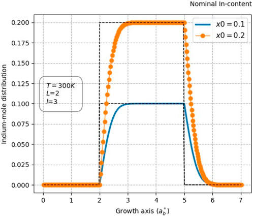
Figure 1. The Indium fraction as a function of the growth axis for two different nominal Indium fractions for a single QW. The dashed line represents their corresponding rectangular profiles. (
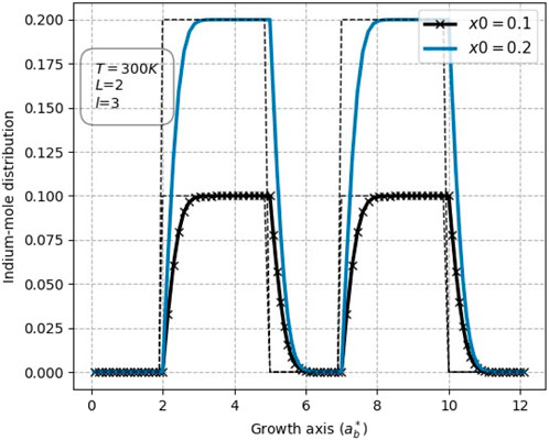
Figure 2. The Indium fraction as a function of the growth axis for two different nominal Inindium fractions for double QWs. The dashed lines represent their corresponding rectangular profiles.
Figure 3 elucidates the alteration of the conduction band profile under the influence of ISS in both strained and unstrained quantum wells, with a nominal indium content of 20% and a well width of
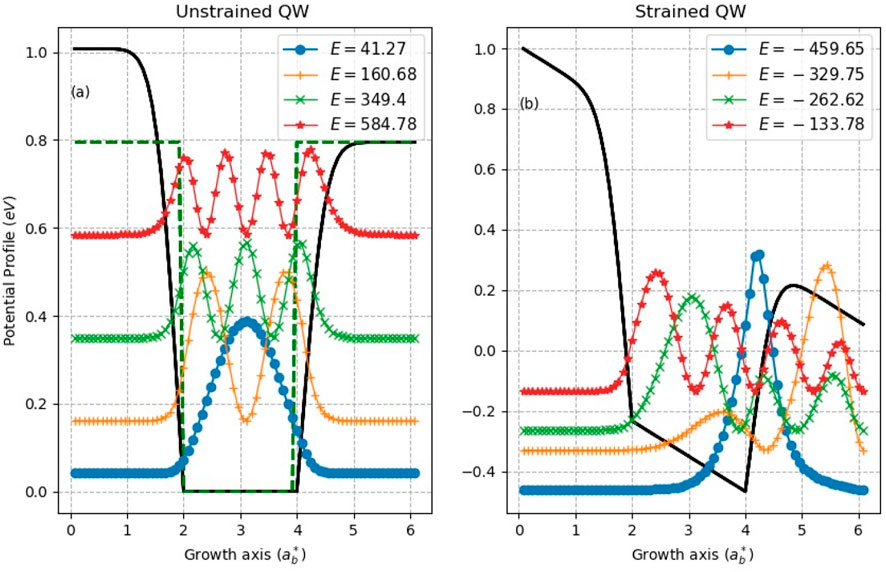
Figure 3. The band structure of strained and unstrained QW, probability densities, and their corresponding eigenvalues for four low-lying states under the effects of ISS for nominal In-content of
Conversely, in Panel (b), the behavior of the strained QW under ISS shows a noteworthy shift in the electron probability densities, particularly for the 1S and 2S subbands, where resonance tunneling facilitates the migration of electron densities towards the right barrier. This shift can be interpreted as a consequence of altered energy landscapes resulting from strain, which can enhance tunneling phenomena and affect carrier lifetimes and relaxation dynamics. The observed energy level modifications underscore the profound influence of strain on electronic transitions. Specifically, the 1S-2S intersubband transition (ISBT) energy experiences a notable increase from 120.5 meV to 145.8 meV, signifying a blue shift of approximately 25.3 meV. This blue shift can be attributed to enhanced confinement effects in the strained QW, which make higher energy states more accessible, thereby improving the efficiency of devices such as quantum cascade lasers and detectors. In stark contrast, the 2P-3S ISBT demonstrates a red shift of about 108.6 meV, suggesting that higher subband states in strained QWs may become less energetically favorable for transitions due to strain-induced modifications in the band structure. The findings on the effects of Intersubband Indium Segregation (ISS) and strain in quantum wells (QWs) demonstrate that tailored strain engineering can significantly modify semiconductor materials’ electronic properties and transition dynamics. The observed blue-shifts in intersubband transition energies under strain indicate enhanced quantum confinement, which may improve efficiency in optoelectronic devices such as quantum cascade lasers and photodetectors. Conversely, the red shifts of higher energy transitions suggest the potential for selective control over electronic states, paving the way for developing advanced materials that exploit strain-induced effects to optimize performance in high-speed electronic and photonic applications.
For nominal In-content of
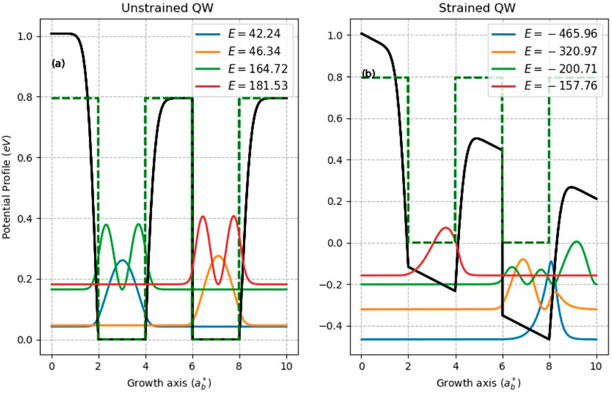
Figure 4. The band structure of strained and unstrained double QWs, probability densities, and their corresponding eigenvalues for four low-lying states under the effects of ISS for nominal In-content of
Based on equation, the ISBT-related absorption coefficient of InxGa1−xN/GaN single and double QWs is governed principally by three parameters. The first is the electron density residing in the initial state, while the second is the energy difference between the initial and final states. The third one is the dipole matrix element representing the overlap of the wave functions between the initial and final states. Figure 5 illustrates the variation of the absorption spectrum according to the photon energy for asymmetric.
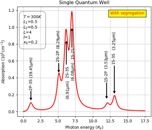
Figure 5. The absorption spectra of asymmetry polar
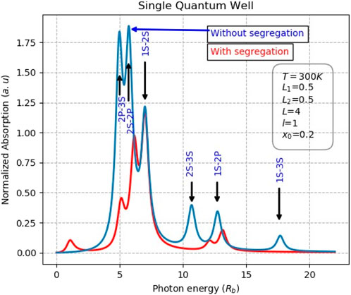
Figure 6. The absorption spectra of asymmetry
The variations of the absorption coefficient as a function of photon energy in asymmetric
Notably, as the nominal indium content varies from 10% to 30%, the 1S-2S and 2S-2P ISBTs become undetectable as their amplitudes drop to two orders of magnitude smaller than those of other transitions. This disappearance of certain transitions under increased indium content indicates a critical threshold where the balance of potential barriers and electronic states is disrupted, leading to diminished absorption characteristics for these specific transitions. Such behavior can significantly influence optoelectronic devices’ overall efficiency and performance based on these materials, as the loss of specific ISBTs could affect the spectral response of devices like photodetectors and lasers. The differential response of each ISBT to changes in nominal indium content further illustrates the complexity of the underlying physics. For instance, the energy of the 2P-3S ISBT shows a blue shift from 4.42 Rb_bb to 5.34 Rb_bb, representing a shift of approximately 26.8 meV (20.8%).
In contrast, the 1S-3S, 1S-2P, and 2S-3S ISBTs experience red shifts of 28%, 44.5%, and 24.6%, respectively. This contrasting behavior can be attributed to the interplay of ISS and the built-in electric field within the QW, which modifies the energy levels by altering the potential relief at the band edges. The ISS effect tends to favor stabilizing certain energy states while destabilizing others, leading to complex absorption spectra reflecting these interactions.
Further insights into the absorption spectra of double quantum wells (DQWs) are provided in Figure 7, which clearly demonstrates that the ISS phenomenon substantially impacts the ISBT-related absorption characteristics. The consistent red shifts observed for all ISBTs when accounting for ISS effects underscore the importance of including such phenomena in the analysis of quantum well systems. To elucidate the significance of these shifts, a comparative analysis with single quantum wells (SQWs) is presented in Table 1, offering a quantitative measure of manner in which Intersubband Indium Segregation (ISS) alters the spectral responses between these two structures. The findings regarding the absorption spectra of asymmetric InGaN/GaN strained quantum wells with 20% of indium compositions highlight the crucial role of nominal indium content and ISS in determining the optical characteristics of semiconductor materials. The observed amplitude drop and the shifting of ISBT energies suggest that careful engineering of indium concentration can tailor the optical response of quantum well structures, optimizing their performance in various optoelectronic applications. The implications of these results underscore the potential for designing advanced devices that leverage strain and ISS effects to achieve desired spectral properties, ultimately leading to enhanced efficiency in applications such as infrared detectors and high-performance lasers.
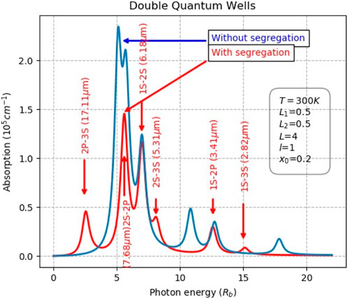
Figure 7. The normalized absorption spectra of asymmetry
The results underscore the critical role of the ISS in achieving more accurate simulation data, particularly for devices that involve high-energy states. The findings suggest that incorporating ISS effects into the modeling of optoelectronic devices is essential for capturing the complexities associated with these high-level states. This is particularly relevant for quantum well structures where precise energy levels and transition probabilities significantly influence device performance. In contrast, neglecting ISS can provide a reasonable approximation for low-energy states, such as the fundamental 1S and 2S states. This discrepancy arises because the deeper states are less sensitive to the deformation of band edges caused by ISS, as illustrated in Figure 1. Moreover, the results presented in Table 1 reveal a notable distinction between single quantum wells (SQWs) and double quantum wells (DQWs) concerning the redshift of ISBT energies under ISS influences. Specifically, the ISBT redshift is more pronounced in SQWs, where the absorption spectra are shifted to lower energies compared to those observed in DQWs. This indicates that the unique confinement and structural characteristics of DQWs mitigate the extent of ISS-induced energy shifts, thereby maintaining more stable transition energies. Interestingly, despite the variations in the spectral displacement due to ISS, the ISBT-related absorption coefficients for the transitions 1S-2S, 2S-2P, and 2P-3S are found to be of comparable magnitude. This characteristic allows for the realization of four-energy-level structures in InGaN/GaN DQWs, emphasizing the potential for these systems to support complex transitions while benefiting from ISS’s mitigating effects. The overall findings corroborate existing literature, although some discrepancies highlight areas for further model exploration and refinement. These insights are particularly promising for designing and optimizing future optoelectronic devices, especially those targeting multiple-color operations within the optical communication wavelength range. The implications of this research point to the potential for tailoring quantum well structures to achieve desired optical characteristics, ultimately contributing to the advancement of high-performance devices suitable for diverse applications in telecommunications and photonics. The findings regarding the significance of the ISS in quantum wells emphasize its necessity in accurately simulating and understanding the optical properties of semiconductor devices. By recognizing the differential impact of ISS on high-energy versus low-energy states, researchers can better design quantum well structures that optimize performance across various applications. The pronounced redshift in ISBTs for SQWs compared to DQWs further suggests that careful structural engineering can enhance the efficacy of optoelectronic devices, particularly for multiple-color applications in optical communication. These results advocate for integrating ISS effects into future design frameworks, ultimately leading to innovations that enhance the functionality and efficiency of next-generation photonic devices. This study presents several limitations that must be acknowledged to understand the findings comprehensively. First, the analysis relies on simplified model assumptions regarding the material properties and behavior of the quantum wells, potentially overlooking complex interactions inherent in real materials. Additionally, the research was conducted at room temperature, limiting insights into how temperature variations could impact the behavior of the ISS and optical absorption.
Furthermore, focusing on a narrow range of indium concentrations (10%–30%) restricts the generalizability of the results; exploring a broader range could yield more comprehensive insights into the effects of indium content. The lack of experimental validation also poses a significant limitation, as real-world data are crucial for corroborating theoretical findings. Lastly, the study does not account for the influence of other phenomena, such as carrier scattering and external electric fields, which could further affect the optical properties. Addressing these limitations in future research will enhance the reliability and applicability of the findings, ultimately leading to improved design and optimization of optoelectronic devices based on nitride materials.
This study employs a one-dimensional (1D) model to investigate the optical transitions in InGaN/GaN quantum wells. While this approach provides key insights into the effects of indium segregation and strain on the intersubband transitions, it is inherently limited in capturing in-plane compositional fluctuations within the quantum wells. These fluctuations can significantly influence carrier energies and localization, affecting wavefunction overlap and optical properties. By accounting for these complexities, we acknowledge that a three-dimensional (3D) model would provide a more comprehensive representation of the material behavior. Implementing a 3D model would refine our understanding of the system and yield results that more closely align with experimental data. Such advancements in modeling could pave the way for improved designs of optoelectronic devices, as it would facilitate a deeper understanding of how varying indium distributions and strain conditions affect device performance.
4 Conclusion
This study analyzes the impact of Indium surface segregation (ISS) on optical absorption related to intersubband transitions (ISBT) in strained IInGaN/GaN single quantum well (SQW) and double quantum well (DQW) structures at room temperature for
Data availability statement
The original contributions presented in the study are included in the article/supplementary material, further inquiries can be directed to the corresponding authors.
Author contributions
HE: Investigation, Software, Validation, Writing–original draft, Writing–review and editing. RE-n: Formal Analysis, Investigation, Methodology, Visualization, Writing–review and editing. MB-M: Conceptualization, Investigation, Validation, Visualization, Writing–review and editing. JI: Data curation, Investigation, Validation, Visualization, Writing–review and editing. AS: Conceptualization, Data curation, Formal Analysis, Resources, Validation, Writing–review and editing.
Funding
The author(s) declare that no financial support was received for the research, authorship, and/or publication of this article.
Conflict of interest
The authors declare that the research was conducted in the absence of any commercial or financial relationships that could be construed as a potential conflict of interest.
Publisher’s note
All claims expressed in this article are solely those of the authors and do not necessarily represent those of their affiliated organizations, or those of the publisher, the editors and the reviewers. Any product that may be evaluated in this article, or claim that may be made by its manufacturer, is not guaranteed or endorsed by the publisher.
References
Auf der Maur, M., Pecchia, A., Penazzi, G., Rodrigues, W., and Di Carlo, A. (2016). Efficiency drop in green inGaN/GaN light emitting diodes: the role of random alloy fluctuations. Phys. Rev. Lett. 116 (2), 027401. doi:10.1103/PhysRevLett.116.027401
Choubani, M., Maaref, H., and Saidi, F. (2022). Indium segregation and In–Ga inter-diffusion effects on the photoluminescence measurements and nonlinear optical properties in lens-shaped InxGa1-xAs/GaAs quantum dots. J. Phys. Chem. Sol. 160, 110360. doi:10.1016/j.jpcs.2021.110360
Dussainge, A., Damilano, B., Grandjean, N., and Massies, J. (2003). In surface segregation in InGaN/GaN quantum wells. J. Cryst. Gr. 251, 471–475. doi:10.1016/S0022-0248(02)02443-0
El Ghazi, H., and John-Peter, A. (2015). Threshold pump intensity effect on the refractive index changes in InGaN SQD: internal constitution and size effects. Phys. B Cond. Mat. 462, 30–33. doi:10.1016/j.physb.2015.01.014
El Ghazi, H., and Jorio, A. (2013). Excited-states of hydrogenic-like impurities in InGaN–GaN spherical QD: electric field effect. Phys. B Condens. Matter 430, 81–83. doi:10.1016/j.physb.2013.08.029
El Ghazi, H., and Jorio, A. (2014). Temperature dependence of interband recombination energy in symmetric (In, Ga) N spherical quantum dot-quantum well. Phys. B Cond. Matt. 432, 64–66. doi:10.1016/j.physb.2013.09.017
En-nadir, R., El Ghazi, H., Belaid, W., Jorio, A., Zorkani, I., and Kiliç, H. Ş. (2021a). Ground and first five low-lying excited states related optical absorption in In. 1Ga. 9N/GaN double quantum wells: temperature and coupling impacts. Solid State Comm. 338, 114464. doi:10.1016/j.ssc.2021.114464
En-Nadir, R., El Ghazi, H., Jorio, A., and Zorkani, I. (2021b). Ground-state shallow-donor binding energy in (In, Ga) N/GaN double QWs under temperature, size, and the impurity position effects. J. Mod. Sim. Mater. 4, 1–6. doi:10.21467/jmsm.4.1.1-6
En-nadir, R., El Ghazi, H., Jorio, A., Zorkani, I., and Kilic, H. S. (2022). Intersubband optical absorption in (In,Ga)N/GaN double quantum wells considering applied electric field effects. J. Comput. Electron 21, 111–118. doi:10.1007/s10825-021-01830-4
Farrell, R. M., Neufeld, C. J., Cruz, S. C., Lang, J. R., Iza, M., Keller, S., et al. (2011). High quantum efficiency InGaN/GaN multiple quantum well solar cells with spectral response extending out to 520 nm. Appl. Phys. Lett. 98, 2011–2014. doi:10.1063/1.3591976
Gmachl, C., Ng, H. M., and Cho, A. Y. (2001). Intersubband absorption in degenerately doped GaN/AlxGa1−xN coupled double quantum wells. Appl. Phys. Lett. 79, 1590–1592. doi:10.1063/1.1403277
Karpov, S.Yu. (2017). Carrier localization in InGaN by composition fluctuations: implication to the “green gap”. Phot. Res. 5, A7–A12. doi:10.1364/PRJ.5.0000A7
Khazanova, S., Bobrov, A., Nezhdanov, A., Sidorenko, K., Baidus, N., Gorshkov, A., et al. (2024). Effects of strain and composition distribution on the optical characteristics of GaAs/InGaAlAs/GaAs double asymmetric tunnel-coupled quantum wells. Opt. Mater. 155, 115825. doi:10.1016/j.optmat.2024.115825
Kumtornkittikul, C., Shimizu, T., Iizuka, N., Suzuki, N., Sugiyama, M., and Nakano, Y. (2007). Fabrication and measurement of AlN cladding AlN/GaN multiple-quantum-well waveguide for all-optical switching devices using intersubband transition. Jpn. J. Appl. Phys. 46, 6639. doi:10.1143/JJAP.46.6639
Laxmi, N., Routray, S., and Pradhan, K. P. (2019). III-Nitride/Si Tandem solar cell for high spectral response: key attributes of auto-tunneling mechanisms. Silicon 12, 2455–2463. doi:10.1007/s12633-019-00342-y
Lei, S. Y., Dong, Z. G., Shen, B., and Zhang, G. Y. (2008). Intersubband transition in symmetric AlxGa1−xN/GaN double quantum wells with applied electric field. Phys. Lett. A 373, 136–139. doi:10.1016/j.physleta.2008.10.091
Lin, S., Zeng, S., Cai, X., Zhang, J., Wu, S., Sun, L., et al. (2012). Simulation of doping levels and deep levels in InGaN-based single-junction solar cell. J. Mat. Sci. 47, 4595–4603. doi:10.1007/s10853-012-6321-6
Lourassi, M., and Soudini, B. (2016). Simulation of piezoelectric and spontaneous polarization effect on the InGaN/Si tandem solar cell. Optik 127, 3091–3094. doi:10.1016/j.ijleo.2015.12.037
Maidaniuk, Y., Kumar, R., Mazur, Y. I., Kuchuk, A. V., Benamara, M., Lytvyn, P. M., et al. (2021). Indium segregation in ultra-thin in (Ga) As/GaAs single quantum wells revealed by photoluminescence spectroscopy. Appl. Phys. Lett. 118, 6. doi:10.1063/5.0039107
Matioli, E., Neufeld, C., Iza, M., Cruz, S. C., Al-Heji, A. A., Chen, X., et al. (2011). High internal and external quantum efficiency InGaN/GaN solar cells. Appl. Phys. Lett. 98, 021102. doi:10.1063/1.3540501
Mayrock, O., Wunsche, H. J., and Henneberger, F. (2000). Polarization charge screening and indium surface segregation in (In,Ga)N/GaN single and multiple quantum wells. Phys. Rev. B 62, 16870–16880. doi:10.1103/PhysRevB.62.16870
Muraki, K., Fukatsu, S., Shiraki, Y., and Ito, R. (1992). Surface segregation of in atoms during molecular beam epitaxy and its influence on the energy levels in InGaAs/GaAs quantum wells. Appl. Phys. Lett. 61, 557–559. doi:10.1063/1.107835
Muraki, K., and FukatsuIto, S. Y. (1992). Surface segregation of in atoms during molecular beam epitaxy and its influence on the energy levels in InGaAs/GaAs quantum wells. Appl. Phys. Lett. 61, 557–560. doi:10.1016/0022-0248(93)90680-U
Nevou, L., Tchernycheva, M., Doyennette, L., Julien, F. H., Warde, E., Colombelli, R., et al. (2006). New developments for nitride unipolar devices at 1.3–1.5 μm wavelengths. Superlattice Microst 40, 412–417. doi:10.1016/j.spmi.2006.09.016
O'Donovan, M., Farrell, P., Moatti, J., Streckenbach, T., Koprucki, T., and Schulz, S. (2024). Impact of random alloy fluctuations on the carrier distribution in multicolor (In,Ga)N/GaN quantum well systems. Phys. Rev. Appl. 21 (2), 024052. doi:10.1103/PhysRevApplied.21.024052
Polyakov, A. Y., Pearton, S., Frenzer, P., Ren, F., Liu, L., and Kim, J. (2013). Radiation effects in GaN materials and devices. J. Mater. Chem. C 1, 877–887. doi:10.1039/C2TC00039C
Rossow, U., Horenburg, P., Ketzer, F., Bremers, H., and Hangleiter, A. (2017). Indium incorporation into InGaN: the role of the adlayer. J. Cryst. Gr. 464, 112–118. doi:10.1016/j.jcrysgro.2017.01.044
Selmi, T., and Belghouthi, R. (2017). A novel widespread Matlab/Simulink based modeling of InGaN double hetero-junction p-i-n solar cell. Int. J. Energy Environ. Eng. 8, 273–281. doi:10.1007/s40095-017-0243-7
Senichev, A., Nguyen, T., Diaz, R. E., Dzuba, B., Shirazi-Hd, M., Cao, Y., et al. (2018). Evolution of indium segregation in metal-polar In0.17Al0.83N lattice-matched to GaN grown by plasma assisted molecular beam epitaxy. J. Cryst. Gr. 500, 52–57. doi:10.1016/j.jcrysgro.2018.08.016
Souaf, M., Baira, M., Maaref, H., and Ilahi, B. (2015). Modelling of the intermixing effects in highly strained asymmetric InGaAs quantum well. Cond. Matter Phys. 18, 1–6. doi:10.5488/CMP.18.33005
Stanlay, I., Coleiny, G., and Venkat, R. (2003). Theoretical study of in desorption and segregation kinetics in MBE growth of InGaAs and InGaN. J. Cryst. Gr. 251, 23–27. doi:10.1016/S0022-0248(02)02406-5
Tchernycheva, M., Nevou, L., Doyennette, L., Julien, F. H., Guillot, F., Monroy, E., et al. (2006). Electron confinement in strongly coupled GaN∕AlN quantum wells. Appl. Phys. Lett. 88, 153113. doi:10.1063/1.2193057
Walukiewicz, W., Ager, J. W., Yu, K. M., Liliental-Weber, Z., Wu, J., Li, S. X., et al. (2006). Structure and electronic properties of InN and In-rich group III-nitride alloys. J. Phys. D. Appl. Phys. 39, R83–R99. doi:10.1088/0022-3727/39/5/R01
Wang, Y., Liang, F., Yang, J., Liu, Z. S., and Zhao, D. (2023). Investigation of the Indium migration mechanism in the growth of InGaN quantum wells by MOCVD. J. Cryst. Gr., 623. 127404 2023. doi:10.3390/cryst13010127
Wu, J., Walukiewicz, W., Yu, K. M., Shan, W., Ager, J. W., Haller, E. E., et al. (2003). Superior radiation resistance of In1-xGa xN alloys: full-solar-spectrum photovoltaic material system. J. Appl. Phys. 94, 6477–6482. doi:10.1063/1.1618353
Keywords: ingan, double quantum wells, strained quantum well, segregation, thin film, multilayers
Citation: El Ghazi H, En-nadir R, Basyooni-M. Kabatas MA, Ibrahim JEFM and Sali A (2024) Effects of indium segregation and strain on near-infrared optical absorption in InGaN/GaN quantum wells. Front. Nanotechnol. 6:1485898. doi: 10.3389/fnano.2024.1485898
Received: 25 August 2024; Accepted: 12 November 2024;
Published: 02 December 2024.
Edited by:
Alexandre Reily Rocha, São Paulo State University, BrazilReviewed by:
Kuldeep Kumar, Career Point University, IndiaStephen Church, The University of Manchester, United Kingdom
Copyright © 2024 El Ghazi, En-nadir, Basyooni-M. Kabatas, Ibrahim and Sali. This is an open-access article distributed under the terms of the Creative Commons Attribution License (CC BY). The use, distribution or reproduction in other forums is permitted, provided the original author(s) and the copyright owner(s) are credited and that the original publication in this journal is cited, in accordance with accepted academic practice. No use, distribution or reproduction is permitted which does not comply with these terms.
*Correspondence: Haddou El Ghazi, aGFkZ2hhemlAZ21haWwuY29t; Mohamed A. Basyooni-M. Kabatas, bS5rYWJhdGFzQHR1ZGVsZnQubmw=, bS5hLmJhc3lvb25pQGdtYWlsLmNvbQ==
 Haddou El Ghazi
 Redouane En-nadir
 Mohamed A. Basyooni-M. Kabatas
 Jamal Eldin F. M. Ibrahim6