
95% of researchers rate our articles as excellent or good
Learn more about the work of our research integrity team to safeguard the quality of each article we publish.
Find out more
ORIGINAL RESEARCH article
Front. Mater. , 19 May 2022
Sec. Semiconducting Materials and Devices
Volume 9 - 2022 | https://doi.org/10.3389/fmats.2022.872909
This article is part of the Research Topic 2021 Retrospective: Semiconducting Materials and Devices View all 4 articles
 Guangchao Zhao1
 Xingli Wang1,2
 Weng Hou Yip1
 Nguyen To Vinh Huy1Philippe Coquet1,2
 Mingqiang Huang3*Beng Kang Tay1,2*
Ternary logic has been proven to carry an information ratio 1.58 times that of binary logic and is capable to reduce circuit interconnections and complexity of operations. However, the excessive transistor count of ternary logic gates has impeded their industry applications for decades. With the modulation of the ferroelectric negative capacitance (NC) properties on the channel potential, MOSFETs show many novel features including steep subthreshold swing and non-saturation output characteristics, based on which an ultra-compact ternary inverter can be achieved. Compared with traditional bulk materials, layered 2D materials and 2D ferroelectrics provide a clean interface and better electrostatic control and reliability. Even though ultra-low SS (∼10 mV/dec) has been experimentally demonstrated in ferroelectric-negative capacitance-incorporated 2D semiconductor (NC2D) FETs, the available models are still rare for large-scale circuit simulations. In this study, the superb electrical properties of pure 2D material stack-based NC2D FETs (layered CuInP2S6 adopted as the 2D ferroelectric layer) are investigated through device modeling based on the Landau–Khalatnikov (LK) equations in HSPICE. We managed to realize an ultra-compact ternary inverter with one NC2D-PMOS (WSe2) and one NC2D-NMOS (MoS2) in HSPICE simulations, whose transistor count is significantly reduced compared with other counterparts. We also proposed a novel input waveform scheme to solve the hysteresis problem caused by ferroelectric modulation to avoid logic confusion. Additionally, the power consumption and propagation delay of the NC2D-based ternary inverter are also investigated. This work may provide some insights into the design and applications of ferroelectric-incorporated 2D semiconductor devices.
Two-dimensional semiconductors including graphene and transition metal dichalcogenides (TMDs) have gained tremendous research interest due to their atomically thin monolayers, which enable better electrostatic control and aggressive scaling capability when adopted as a channel material in future field-effect transistor (FET) fabrication (Radisavljevic et al., 2011; Desai et al., 2016). However, it is still hard to achieve a sub 60 mV/dec subthreshold swing (SS) without incorporating extra gate stack modulation due to the so-called Boltzmann tyranny (Salahuddin and Datta, 2008; Taur and Ning, 2013).
Owing to the negative capacitance (NC) features of ferroelectrics, ultra-steep SS has been demonstrated on both silicon-based and 2D-based FETs by incorporating a ferroelectric layer such as hafnium zirconium oxide Hf0.5Zr0.5O2 (HZO) or P(VDF-TrFE) polymer (McGuire et al., 2016; McGuire et al., 2017; Si et al., 2017). By eliminating the interface traps caused by dangling bonds and charged impurities, layered ferroelectrics CuInP2S6 (CIPS) with atomically flat surfaces may offer superior performance and reliability for NC-FETs as compared to bulk ferroelectrics. Recently, a low SS (sub 30 mV/dec) has been achieved in CIPS-based NC2D FET, which will further reduce the power consumption during logic state transition. Thus, it will facilitate its industry applications such as logic and memory devices (Si et al., 2018; Wang et al., 2019; Wang et al., 2021).
To analyze the operation principles of NC2D devices and to build up high-level circuit simulation, SPICE models are highly in demand. However, the available result for NC2D modeling, especially the CIPS-based NC2D FET model, is quite rare. In this work, customized compact Verilog-A models based on the time-dependent LK equations have been established for the CIPS-based NC2D FETs and validated with experimental data. By tuning the parameter associated with the MOS capacitance and negative capacitance of the ferroelectric layer, the model is compatible with different sets of LK coefficients, which can be extracted from experimental electric field-polarization (EP) tests. Several NC2D FET features including ultra-steep SS, drain voltage–induced negative differential resistance, and internal gate voltage amplification have been explored and discussed. Additionally, with the availability of the NC2D FET compact models, an ultra-compact ternary inverter with the same structure as its CMOS binary counterpart has been demonstrated and analyzed through HSPICE simulation.
In this study, the NC2D FET adopts a purely 2D material-based metal-ferroelectric-metal-insulator-semiconductor (MFMIS) structure, in which the 2D ferroelectric CuInP2S6 (CIPS) was added to the gate stack in a conventional 2D semiconductor FET structure (Figure 1). The NC2D FET compact model was established by solving charge and potential equilibrium equations between the ferroelectric layer and the channel of the baseline FET self-consistently in HSPICE, as shown in Figure 2A.
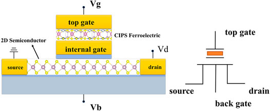
FIGURE 1. Structure and circuit symbol of the NC2D FET. 2D CIPS is adopted in the top gate stack as the ferroelectric negative capacitance layer.
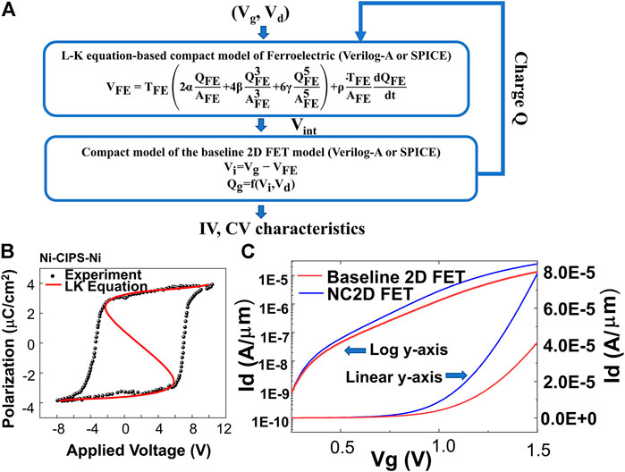
FIGURE 2. Device modeling method of the NC2D FET. (A) Modeling flow of the NC2D FETs. (B) LK coefficient extraction from the previous EP test of the 2D CIPS ferroelectric, α = −6.59E10 cm/F, β = 6.21E21 cm2/F/C2, and γ = 1.15E11 cm9/F/C4. (C) Transfer characteristic comparison between the 2D FETs with/without CIPS incorporation with log y-axis in the left and linear y-axis in the right.
The ferroelectric layer was modeled as a capacitor whose charge and voltage dependence relation were defined by the time-dependent LK equation (Lo, 2003; Salahuddin and Datta, 2008; Aziz et al., 2016) given as follows:
Here,
Figure 2C shows the comparison of the simulated transfer characteristics of the MoS2 FET with and without the ferroelectric CIPS stack incorporation. Similar to the experimental demonstrations of both bulk and 2D semiconductors, the overall current level of the NC2D devices is improved due to the internal voltage amplification compared with the underlying transistor without the ferroelectric stack. This can be explained based on the principle Vi = Vg - VFE (Huang et al., 2020). When the FET works in the second and third quadrant of the ferroelectric S curve (also known as the negative capacitance region due to the reverse relation between charge and voltage), the CIPS layer voltage will be negative, which makes the underlying internal gate voltage to be larger than the applied top gate voltage. It is worth mentioning that when zero top gate voltage is applied, the FET will operate in the first and fourth quadrant, where CIPS layer voltage VFE will be positive and the underlying internal gate voltage Vi be negative. This will further depress the off-state current; thus the on/off ratio of NC2D FETs will be improved.
In a typical silicon FET, SS can be mathematically described as follows:
where CMOS is the MOSFET gate capacitance, and Cox is the gate dielectric capacitance (Wouters et al., 1990). Typically, positive CMOS and Cox will result in SS being always larger than the Boltzmann limit: 60 mV/dec (
In this work, we also investigated the dependence of SS improvement of NC2D FETs on the thickness of CIPS. The average SS is defined and determined by extracting the slope of the IdVg curve over the whole subthreshold region in this work, as shown in the inset in Figure 3A. Figure 3A shows the simulated results compared with the numerical calculation of SS with a ferroelectric layer of different thicknesses. It is obvious that as the thickness increases, SS tends to decrease, speeding up the transistor on/off transition rate. This is mainly due to the capacitance matching between the negative capacitance and the MOS capacitance. With increasing thickness, the absolute value of negative capacitance will decrease, which also increases the absolute value of
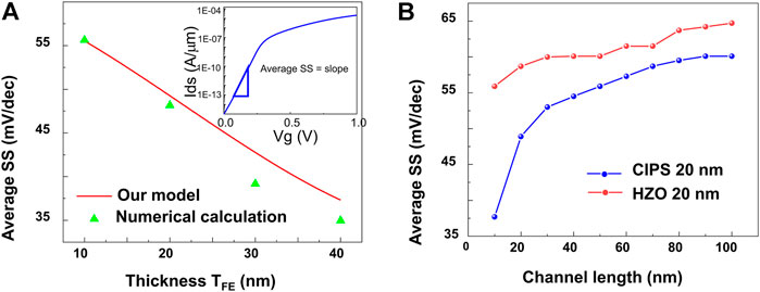
FIGURE 3. Average subthreshold swing results and comparisons. The average SS is defined and determined by extracting the slope of transfer characteristic over the whole subthreshold region in this work. (A) Average SS of the NC2D FETs with varying ferroelectric layer thickness. The red line is our established model, and the green dots are the numerical calculations of previous works. (B) Average SS along with channel length scaling with 20 nm CIPS and 20 nm HZO incorporation.
In order to show the superiority of the CIPS ferroelectric compared with traditional HZO, we presented the average SS of NCFET by incorporating the two kinds of ferroelectrics. The dependence of the average SS on different channel lengths with 20 nm CPIS and HZO incorporation is presented in Figure 3B. Based on the simulations, CIPS shows better SS improvement than HZO [LK coefficients of HZO are from (Jiang et al., 2018)] of the same thickness. This is due to the fact that based on the extracted LK coefficients, the CIPS ferroelectric will have better capacitance matching with the underlying MOSFET gate capacitance than HZO. Another intriguing phenomenon shown in Figure 3B is that the average SS will decrease with the decrease in the channel length, which is quite different from conventional transistors. A similar finding has been demonstrated in experiments by Wang et al. (2020). Such an effect can be explained as follows: with the decrease in the channel length, the drain terminal capacitive coupling effect will become larger, resulting in larger CMOS and a smaller difference between Cox and CMOS (Kwon et al., 2018). These emerging effects indicate a promising advancement of negative capacitance in semiconductor industry applications, which have been limited by the difficulties in turning off the current (the main roadblock of transistor scaling) and keeping Moore’s law effective.
Drain voltage-induced negative differential resistance (NDR) is a distinctive phenomenon of NC FETs (Zhou et al., 2018; Alam et al., 2019). Drain current will decrease with drain voltage if NDR happens, which is quite different from the traditional drain field-induced potential barrier lowering effect (DIBL). NDR happens due to the drain voltage coupling effect:
where
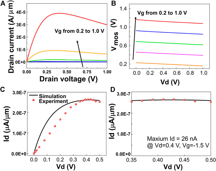
FIGURE 4. NDR effect in device modeling. (A) NDR effects in the simulated output characteristics of NC2D FETs under different gate voltages. (B) Simulated underlying MOSFET gate voltage VMOS (internal voltage); the same color means under the same condition with (A). (C) Simulated NDR effect against the experimental measurement of CIPS incorporated NC2D FETs. (D) Simulation results against experiments in the NDR region.
Recently, the NDR effect has also been observed in CIPS-based NC2D FETs (Ye, 2018). In this work, we have also tried to simulate and engineer the NDR effect in our model. In Figure 4C, the simulated output curve in which NDR happens when Vd > 0.4 V is validated against the experimental data (Wang et al., 2019). The same device structure is adopted. For simplicity, we treated graphene as metal in our simulation, which was used to fabricate the internal gate in their work. Our model fits well with the experimental data within the NDR region. The discrepancies between the simulation curve and experiment in the low drain voltage region are believed to be caused by voltage division on the contact, which will delay the saturation effect and lower the overall current level. Additionally, the irregularly shaped physical geometries of the fabricated devices may also account for such discrepancies.
The ternary logic system carries an information ratio 1.58 times that of its binary counterpart and is possible to reduce the circuit complexity, chip area, and increase the processing rate (Hurst, 1984; Wu and Prosser, 1990; Vudadha and Srinivas, 2018; Huang et al., 2019). However, the traditional realization of ternary logics suffers from the exceeding number of transistors or resistors, which severely offsets its superiority (da Silva et al., 2006). In 2017, an inverter based on ferroelectric FETs generated a gain-loss region in the voltage transfer curve (VTC) (Gupta et al., 2017). By utilizing this property and further adjusting the capacitance matching, we can achieve a ternary inverter with the same structure as its CMOS binary counterpart.
Based on the established n-type and p-type CIPS NC2D FET Verilog-A compact models, we have demonstrated a standard ternary inverter with an ultra-compact structure in HSPICE. The basic schematic representation is shown in Figure 5A, where MoS2 and WSe2 are chosen as the n-type and p-type semiconductors, respectively. Figure 5B shows the VTC simulation results of the NC2D-based ternary inverter incorporated with different thicknesses of the ferroelectric layer (5, 10, 15, 20, and 25 nm). An intermediate state of 0.5 V appears distinctly when the input voltage is over 0.4 V with a supply voltage of 1.0 V. With the thickness of CIPS increasing, both 1→1/2 and 1/2→0 logic level transition points will shift right. This is also reflected in the DC gain of the ternary inverter presented in Figure 5C. The DC gain curves are obtained by the derivative dVout/dVin. For a given DC curve, the first peak corresponds to 1→1/2 logic level transition, and the second peak corresponds to 1/2→0 logic level transition. As can be seen in Figure 5C, with increasing thickness, the peak of the gain curve will shift right with larger amplitude. A larger DC gain is usually expected, which means a narrower logic level transition zone will help reduce the dynamic power consumption. Also, the voltage gain of the inverter will increase with its thickness, which indicates an improvement in the logic level transition rate and noise margin. Our further load-line analysis presented in Figure 5D indicates that the middle state is generated due to intersections of the transistor IV curves under the same input voltage (operation points) in the middle region. The underlying reasons are the non-saturation and aggregation effects of the NC2D FET transfer characteristic, which are due to the internal gate voltage amplification caused by CIPS ferroelectric modulations.
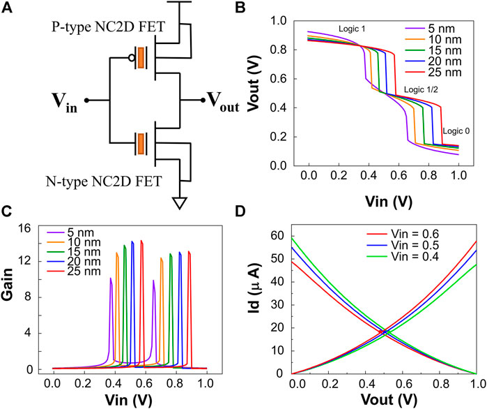
FIGURE 5. Ultra-compact ternary inverter based on NC2D FETs. (A) Schematic representation of the simulated ultra-compact ternary inverter. (B) VTC of the ternary inverter with CIPS of different thicknesses. (C) DC gain of the ternary inverter. (D). Load-line analysis of the ternary inverter.
Hysteresis is observed in the dual DC sweep of the ternary inverter, as shown in Figure 6A. Figure 6B shows the load-line analysis of the proposed ternary inverter. The IV curve in the left branch from 0 to 1 V is the output characteristic of the n-type NC2D FET, while the IV curve in the right branch from 1 to 0 V is the output characteristic of the p-type NC2D FET. The same color represents the IV curves under the same input voltage, and the cross points are the corresponding operation points (OP), whose x-axis value will generate the output of the ternary inverter. The reason for the generation of the hysteresis can be explained as follows: for a given input voltage, the ternary inverter actually has one different operation point during the forward and reverse sweep due to the NDR effect of the NC2D FETs. Considering 0.6 V input voltage as an example, under the forward sweep condition (sweep input voltage from 0 to 1 V), the operation point is OP2, generating 0.5 V output voltage; however, in the reverse sweep condition (sweep input voltage from 1 to 0 V), the operation point is OP1, generating 0.15 V output voltage. Similarly, when the input voltage is 0.4 V, the operation points will be OP4 in the forward sweep but OP3 in the reverse sweep, generating different output voltages.
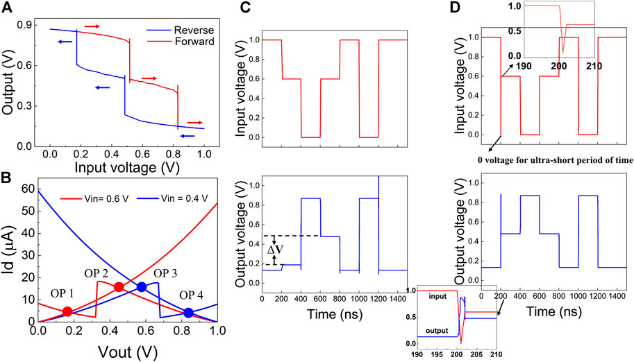
FIGURE 6. Analysis and solution to the hysteresis problem. (A) Dual DC sweep of the NC2D-based ternary inverter. (B) Load-line analysis of the hysteresis of the ternary inverter. (C) Transient simulations of the NC2D-based ternary inverter using the traditional input waveform. (D). Transient simulations of the NC2D-based ternary inverter using the new input waveform scheme. The aforementioned inset is the zoom-in details of the added negative pulse. The following inset shows the zoom-in rise and fall details when the inverter crosses the hysteresis region at around 200 ns (0–1 logic level transition).
We further performed transient analysis to investigate the propagation delay and power consumption of the proposed ternary inverter. For the transient simulations, 25 nm CIPS is chosen to guarantee the inverter to have a middle state at around 0.5 V with a 0.6 V input signal. We used a piecewise linear waveform as the stimulus, and the switch between states takes 5.0 ns. Different from the binary inverter, the ternary input waveform should cover much more transition conditions: (0 → 1/2, 1/2→1, 1→1/2, 1/2→0, 0→1, and 1→0). As shown in Figure 6C, the red waveform used as the input signal covers all the logic level transition conditions. The blue waveform is the corresponding output of the ternary inverter. Both the high and low input logic levels are correctly mapped into low and high output logic levels, respectively. However, owing to the hysteresis effect mentioned earlier, the output middle logic levels are not balanced under different transition conditions. In order to solve the hysteresis problem and avoid logic confusion in the functional ternary systems, we proposed a novel input waveform scheme, as shown in Figure 6D (red waveform). The main idea is to adjust the input waveform during which the hysteresis will occur, that is, 1→1/2 transition condition. We reprogrammed the input waveform to apply 0 voltage for a significantly short period of time (0.1 ns) just before the logic transition from 1 to 1/2 occurs (details shown in the inset before Figure 6D). A pulse duration of 0.1 ns is determined by the highest ferroelectric switch time reported in Li et al. (2004). It should be noted that this work only demonstrates a prototype ideal of using such a method to solve the hysteresis problem. A larger negative pulse amplitude or longer duration time will be needed if the ferroelectric operation frequency is lower. The nanosecond of 0 voltage facilitates the input waveform to cross the hysteresis region swiftly and will have no effect on the logic output. The red waveform in Figure 6D shows the corresponding output with a clear output middle state under the new input waveform scheme. The inset below Figure 6D shows the zoom-in rise and fall details when the inverter crosses the hysteresis region at around 200 ns (0–1 logic level transition).
We have also measured the power consumption and propagation delay using the inbuilt modules in HSPICE. The methodology used in CMOS binary inverter analysis is adopted in our calculations (Calhoun et al., 2008). Moreover, all the different logic transition conditions are considered. The maximum delay is measured to be 1.96 ns during the 1→1/2 transition, which can be easily understood due to the adjustment that we have made to get the new input waveform scheme. The average power consumption is measured to be 8.0957 uW. Therefore, the power–delay product (PDP) is 15.87 fJ, which is close to the standard CMOS binary inverters and a promising candidate for future industrial applications.
In this study, CIPS-based NC2D FET Verilog-A compact models have been established and validated on the experimental data. Some of the feature effects observed in experiments including SS improvement, NDR, and current level improvement have been analyzed and repeated in our models. An ultra-compact ternary inverter has been successfully demonstrated based on pure 2D MFMIS structures through HSPICE simulations, whose intermediate state can be tuned by adjusting the ferroelectric thickness. We have also proposed a novel input waveform scheme to solve the hysteresis problem, which may cause severe logic confusion in ferroelectric-based logic systems. In addition, some critical parameters including power consumption, propagation delay, and PDP are investigated and compared. We believe this work will shed light on the future applications of 2D ferroelectric-incorporated 2D semiconductors, especially in the realization of ternary logics and other low-power circuit designs.
The raw data supporting the conclusion of this article will be made available by the authors, without undue reservation.
BT, MH, and GZ conceived and designed the project. GZ established the compact model. GZ and NH performed the DC and transient analysis of the ternary logic gates. XW was responsible for collecting the experimental data. The article was written by GZ and revised by WY, XW, and PC.
This research work was supported by the Ministry of Education, Singapore, under its MOE Tier 2 project (MOE2019-T2-2-075), Shenzhen Science and Technology Innovation Committee JCYJ20200109115210307, and Guangdong Basic and Applied Basic Research Foundation 2019A1515111142, China.
The authors declare that the research was conducted in the absence of any commercial or financial relationships that could be construed as a potential conflict of interest.
All claims expressed in this article are solely those of the authors and do not necessarily represent those of their affiliated organizations, or those of the publisher, the editors, and the reviewers. Any product that may be evaluated in this article, or claim that may be made by its manufacturer, is not guaranteed or endorsed by the publisher.
Alam, M. A., Si, M., and Ye, P. D. (2019). A Critical Review of Recent Progress on Negative Capacitance Field-Effect Transistors. Appl. Phys. Lett. 114, 090401. doi:10.1063/1.5092684
Aziz, A., Ghosh, S., Datta, S., and Gupta, S. (2016). Physics-based Circuit-Compatible SPICE Model for Ferroelectric Transistors. IEEE Electron Device Lett. 37 (6), 1. doi:10.1109/LED.2016.2558149
Beckers, A., Jazaeri, F., and Enz, C. (2020). Theoretical Limit of Low Temperature Subthreshold Swing in Field-Effect Transistors. IEEE Electron Device Lett. 41 (2), 276–279. doi:10.1109/LED.2019.2963379
Calhoun, B. H., Yu Cao, Y., Xin Li, X., Ken Mai, K., Pileggi, L. T., Rutenbar, R. A., et al. (2008). Digital Circuit Design Challenges and Opportunities in the Era of Nanoscale CMOS. Proc. IEEE 96 (2), 343–365. doi:10.1109/JPROC.2007.911072
da Silva, R. C. G., Boudinov, H., and Carro, L. (2006). A Novel Voltage-Mode CMOS Quaternary Logic Design. IEEE Trans. Electron Devices 53 (6), 1480–1483. doi:10.1109/TED.2006.874751
Desai, S. B., Madhvapathy, S. R., Sachid, A. B., Llinas, J. P., Wang, Q., Ahn, G. H., et al. (2016). MoS 2 Transistors with 1-nanometer Gate Lengths. Science 354 (6308), 99–102. doi:10.1126/science.aah4698
Gupta, S., Steiner, M., Aziz, A., Narayanan, V., Datta, S., and Gupta, S. K. (2017). Device-circuit Analysis of Ferroelectric FETs for Low-Power Logic. IEEE Trans. Electron Devices 64 (8), 3092–3100. doi:10.1109/TED.2017.2717929
Huang, M., Wang, X., Zhao, G., Coquet, P., and Tay, B. (2019). Design and Implementation of Ternary Logic Integrated Circuits by Using Novel Two-Dimensional Materials. Appl. Sci. 9 (20), 4212. doi:10.3390/app9204212
Huang, W., Zhu, H., Jia, K., Wu, Z., Yin, X., Huo, Q., et al. (2020). Investigation of Device-Circuit for Negative Capacitance Vertical Nanowire FETs Based on SPICE Model. Semicond. Sci. Technol. 35 (8), 085018. doi:10.1088/1361-6641/ab8e0e
Hurst, S. L. (1984). Multiple-Valued Logic-Its Status and its Future. IEEE Trans. Comput. C-33 (12), 1160–1179. doi:10.1109/TC.1984.1676392
Jiang, C., Si, M., Liang, R., Xu, J., Ye, P. D., and Alam, M. A. (2018). A Closed Form Analytical Model of Back-Gated 2-D Semiconductor Negative Capacitance Field Effect Transistors. IEEE J. Electron Devices Soc. 6, 189–194. doi:10.1109/JEDS.2017.2787137
Jin, C., Saraya, T., Hiramoto, T., and Kobayashi, M. (2020). Physical Mechanisms of Reverse DIBL and NDR in FeFETs with Steep Subthreshold Swing. IEEE J. Electron Devices Soc. 8, 429–434. doi:10.1109/JEDS.2020.2986345
Kwon, D., Chatterjee, K., Tan, A. J., Yadav, A. K., Zhou, H., Sachid, A. B., Reis, R. D., Hu, C., and Salahuddin, S. (2018). Improved Subthreshold Swing and Short Channel Effect in FDSOI N-Channel Negative Capacitance Field Effect Transistors. IEEE Electron Device Lett. 39 (2), 300–303. doi:10.1109/LED.2017.2787063
Lee, M. H., Chen, K.-T., Liao, C.-Y., Gu, S.-S., Siang, G.-Y., Chou, Y.-C., et al. (2018). “Extremely Steep Switch of Negative-Capacitance Nanosheet GAA-FETs and FinFETs,” in 2018 IEEE International Electron Devices Meeting (IEDM) (IEEE), 31.8. 1–31.8. 4. doi:10.1109/IEDM.2018.8614510
Li, J., Nagaraj, B., Liang, H., Cao, W., Lee, C. H., and Ramesh, R. (2004). Ultrafast Polarization Switching in Thin-Film Ferroelectrics. Appl. Phys. Lett. 84 (7), 1174–1176. doi:10.1063/1.1644917
Li, K.-S., Chen, P.-G., Lai, T.-Y., Lin, C.-H., Cheng, C.-C., Chen, C.-C., et al. (2015). “Sub-60mV-swing Negative-Capacitance FinFET without Hysteresis,” in 2015 IEEE International Electron Devices Meeting (IEDM) (IEEE), 22.6. 1–22.6. 4. doi:10.1109/IEDM.2015.7409760
Lo, V. C. (2003). Simulation of Thickness Effect in Thin Ferroelectric Films Using Landau-Khalatnikov Theory. J. Appl. Phys. 94 (5), 3353–3359. doi:10.1063/1.1598275
McGuire, F. A., Cheng, Z., Price, K., and Franklin, A. D. (2016). Sub-60 mV/decade Switching in 2D Negative Capacitance Field-Effect Transistors with Integrated Ferroelectric Polymer. Appl. Phys. Lett. 109 (9), 093101. doi:10.1063/1.4961108
McGuire, F. A., Lin, Y.-C., Price, K., Rayner, G. B., Khandelwal, S., Salahuddin, S., et al. (2017). Sustained Sub-60 mV/decade Switching via the Negative Capacitance Effect in MoS2 Transistors. Nano Lett. 17 (8), 4801–4806. doi:10.1021/acs.nanolett.7b01584
Radisavljevic, B., Radenovic, A., Brivio, J., Giacometti, V., and Kis, A. (2011). Single-layer MoS2 Transistors. Nat. Nanotech 6 (3), 147–150. doi:10.1038/nnano.2010.279
Salahuddin, S., and Datta, S. (2008). Use of Negative Capacitance to Provide Voltage Amplification for Low Power Nanoscale Devices. Nano Lett. 8 (2), 405–410. doi:10.1021/nl071804g
Si, M., Jiang, C., Su, C.-J., Tang, Y.-T., Yang, L., Chung, W., et al. (2017). “Sub-60 mV/dec Ferroelectric HZO MoS2 Negative Capacitance Field-Effect Transistor with Internal Metal Gate: The Role of Parasitic Capacitance,” in 2017 IEEE International Electron Devices Meeting (IEDM), (IEEE), 23.5. 1–23.5. 4. doi:10.1109/IEDM.2017.8268447
Si, M., Liao, P.-Y., Qiu, G., Duan, Y., and Ye, P. D. (2018). Ferroelectric Field-Effect Transistors Based on MoS2 and CuInP2S6 Two-Dimensional van der Waals Heterostructure. Acs Nano 12 (7), 6700–6705. doi:10.1021/acsnano.8b01810
Taur, Y., and Ning, T. H. (2013). Fundamentals of Modern VLSI Devices. United Kingdom: Cambridge University Press. doi:10.1017/cbo9781139195065.005
Vudadha, C. K., and Srinivas, M. (2018). “Design Methodologies for Ternary Logic Circuits,” in 2018 IEEE 48th International Symposium on Multiple-Valued Logic (ISMVL), May. 2018 (IEEE), 192–197. doi:10.1109/ISMVL.2018.00041
Wang, X., Yu, P., Lei, Z., Zhu, C., Cao, X., Liu, F., et al. (2019). Van der Waals negative capacitance transistors. Nat. Commun. 10 (1), 1–8. doi:10.1038/s41467-019-10738-4
Wang, X., Zhu, C., Deng, Y., Duan, R., Chen, J., Zeng, Q., et al. (2021). Van der Waals engineering of ferroelectric heterostructures for long-retention memory. Nat. Commun. 12 (1), 1–8. doi:10.1038/s41467-021-21320-2
Wang, Y., Bai, X., Chu, J., Wang, H., Rao, G., Pan, X., et al. (2020). Record‐Low Subthreshold‐Swing Negative‐Capacitance 2D Field‐Effect Transistors. Adv. Mat. 32 (46), 2005353. doi:10.1002/adma.202005353
Wouters, D. J., Colinge, J.-P., and Maes, H. E. (1990). Subthreshold Slope in Thin-Film SOI MOSFETs. IEEE Trans. Electron Devices 37 (9), 2022–2033. doi:10.1109/16.57165
Wu, X. W., and Prosser, F. P. (1990). CMOS Ternary Logic Circuits. IEE Proc. F. Radar Signal Process. U. K. 137 (1), 21–27. doi:10.1049/ip-g-2.1990.0005
Ye, P. D. (2018). “Steep-Slope Hysteresis-free Negative-Capacitance 2D Transistors,” in 2018 76th Device Research Conference (DRC) (IEEE), 1. doi:10.1109/ICSICT.2018.8564814
Keywords: ternary logics, 2D semiconductors, ferroelectrics, negative capacitance, device modeling
Citation: Zhao G, Wang X, Yip WH, Vinh Huy NT, Coquet P, Huang M and Tay BK (2022) Ternary Logics Based on 2D Ferroelectric-Incorporated 2D Semiconductor Field Effect Transistors. Front. Mater. 9:872909. doi: 10.3389/fmats.2022.872909
Received: 10 February 2022; Accepted: 14 April 2022;
Published: 19 May 2022.
Edited by:
Peide Ye, Purdue University, United StatesReviewed by:
Huamin Li, University at Buffalo, United StatesCopyright © 2022 Zhao, Wang, Yip, Vinh Huy, Coquet, Huang and Tay. This is an open-access article distributed under the terms of the Creative Commons Attribution License (CC BY). The use, distribution or reproduction in other forums is permitted, provided the original author(s) and the copyright owner(s) are credited and that the original publication in this journal is cited, in accordance with accepted academic practice. No use, distribution or reproduction is permitted which does not comply with these terms.
*Correspondence: Beng Kang Tay, RUJLVEFZQG50dS5lZHUuc2c=; Mingqiang Huang, bXEuaHVhbmcyQHNpYXQuYWMuY24=
Disclaimer: All claims expressed in this article are solely those of the authors and do not necessarily represent those of their affiliated organizations, or those of the publisher, the editors and the reviewers. Any product that may be evaluated in this article or claim that may be made by its manufacturer is not guaranteed or endorsed by the publisher.
Research integrity at Frontiers
Learn more about the work of our research integrity team to safeguard the quality of each article we publish.