 Dongdong D. Meng
 Xueqiang Q. Ji3,4†
95% of researchers rate our articles as excellent or good
Learn more about the work of our research integrity team to safeguard the quality of each article we publish.
Find out more
ORIGINAL RESEARCH article
Front. Mater. , 18 June 2021
Sec. Semiconducting Materials and Devices
Volume 8 - 2021 | https://doi.org/10.3389/fmats.2021.672128
This article is part of the Research Topic 2021 Retrospective: Semiconducting Materials and Devices View all 4 articles
Monoclinic Ga2O3 (β-Ga2O3) films were grown on Si/SiO2 by using MOCVD. Then, we fabricated the solar-blind photodetector with a back-gate MOS structure. The device exhibited obvious photoresponse under 254-nm UV light illumination, and the photocurrent increased by five orders of magnitude, which could be controlled by VGS. The current generated under dark conditions could also be regulated by VGS and tended to constant when the regulation of VGS was reaching saturation. Meanwhile, VGS was confirmed to have a certain ability to regulate the photocurrent. The present device demonstrated excellent stability and fast response (rise) and recovery (decay) times under the 254-nm light illumination as well as a responsivity of 417.5 A/W, suggesting a valuable application in solar-blind UV photodetectors.
Owing to their wide bandgap (∼4.9 eV) and stable chemical and physical properties, β-Ga2O3 thin films have been investigated for use as ultraviolet (UV) photodetectors (PDs) (Kokubun et al., 2007; Oshima et al., 2008). In the literature, PDs have received extensive attention for the applications in fire detection, missile tracking, radiation detection, and ozone hole monitoring (Monroy et al., 2003; Alaie et al., 2015). Meanwhile, the characteristics of the solar-blind UV PDs based on the β-Ga2O3 films, such as responsivity, selectivity, quantum efficiency, and stability, have been reported. O. Sooyeoun et al. have demonstrated that the Si-implanted β-Ga2O3 PD had a responsivity of 1.45 A/W, and the rise and decay time constants were calculated to be 0.58/32.93 and 1.2/32.86 s, respectively (Sooyeoun et al., 2015). Y. Xu et al. have demonstrated that the β-Ga2O3 PD grown on sapphire using the mist-CVD method exhibited a spectral responsivity of 150 A/W, and the external quantum efficiency was over 7 × 10⁴% (Xu et al., 2018). S. Nakagomi et al. fabricated a deep UV photodiode using a heterojunction between the β-Ga2O3 layer and the 6H-SiC substrate and obtained blazing response speeds. The time constants were estimated to be 1.2 and 1.5 ms (Nakagomi et al., 2013), which were superior to the response time constants of all the above-mentioned reports, while the current was unstable in the range of light pulses.
Although many fabrication technologies have been used to improve the β-Ga2O3 PDs’ quality, the film-type PDs’ photoresponses are still not their best performances, so that limits the practical application. In this work, we have prepared high-quality β-Ga2O3 films using the MOCVD method. The most significant advantage of this technology is that a low-resistance Ohmic contact between the β-Ga2O3 film and the electrode can be formed, thus reducing the influence on the flow of photoinduced carriers. Meanwhile, a solar-blind UV PD with a back-gate MOS structure was fabricated, and the photoresponse behaviors based on different applied voltages under dark and illumination conditions were characterized. Such detectors with a back-gate MOS structure fabricated on β-Ga2O3 films show high responsivity and fast response times, which can also be regulated by adjusting the gate voltages and drain voltages.
The β-Ga2O3 film was grown unintentionally doped (UID) on Si/SiO2 substrate with a diameter of 2 inches using the metal organic chemical vapor deposition (MOCVD) method. The growth temperature was set to 690 °C, and the chamber pressure was held at 25 Torr. Trimethylgallium (TEGa) and high-purity oxygen were used as the gallium and oxygen precursors, respectively, and Ar was used as the carrier gas. Compared with other CVD growth methods, the MOCVD method could obtain high-quality films. All samples were cleaned successively with acetone, alcohol, and deionized water for 10 min to get ready for the transistor.
The interdigital Ti/Au electrodes were deposited on the β-Ga2O3 film using a shadow mask by radio frequency magnetron sputtering, with a power of 100 W, a pressure of 1 Pa, and an argon gas ratio of 30 SCCM, and then we obtained the back-gate MOS structure PD. All films and devices were fabricated at Beijing Gallium Family Technology, Co., Ltd. Figure 1A shows the schematic cross section of the fabricated β-Ga2O3 film device, including the SiO2 dielectric layer of 100 nm, the grown β-Ga2O3 film of 400 nm, and the deposition of interdigital Ti/Au (30/70 nm) electrodes. The schematic diagram of the fabricated β-Ga2O3 film device with the back-gate MOS structure from the top-right view is shown in Figure 1B. This is a typical three-terminal MOS structure including the source side, which is generally used as a ground unit (GNDU); the gate, which is usually connected to an SMU power supply (SMU1); and the drain side (SMU2), which is also a power supply with working voltage. It is worth noting that the present device will convert into a typical MSM detector when the gate voltage is not applied (SMU1 = 0).
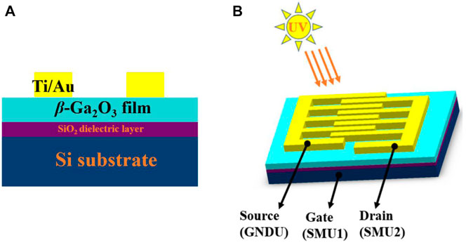
FIGURE 1. (Color online) (A) Schematic cross section. (B) Schematic diagram of the fabricated β-Ga2O3 film device with the back-gate MOS structure.
The interdigital electrode patterns are 2 × 2 mm2. In detail, the metal electrode possession area is removed, and the effective photosensitive area is 1 mm2 for the sample. As reported, the electron affinity of Ga2O3 is 4.00 ± 0.05 eV, and the work function of Ti is 4.33 eV. Therefore, according to the Schottky–Mott rule, the metal–semiconductor (MS) interface barriers of Ti/β-Ga2O3 are approximately 0.33 eV, suggesting an approximate Ohmic contact between metal Ti and semiconductor β-Ga2O3. It ensures that the electrode contact will not interfere with the photoelectric performance of the device as much as possible.
The current–voltage (I–V) and time-dependent photoresponse of the β-Ga2O3 film detector were measured using a Keithely 4,200. The UV response measurement was performed using a 6-W UV lamp, which was used as a light source to provide illumination of wavelengths 254 and 365 nm. The time-dependent photoresponse measurement was performed at a fixed voltage of 10 V. All the measurements were carried out at room temperature.
As shown in Figure 2, the grown layer exhibited a smooth surface morphology with a root mean square (RMS) roughness of 0.54 nm, which was determined from the 2D AFM image over a 5 × 5-μm2 scan area. Obviously, the β-Ga2O3 film has uniformly grown on the Si/SiO2 substrate using the MOCVD growth method.
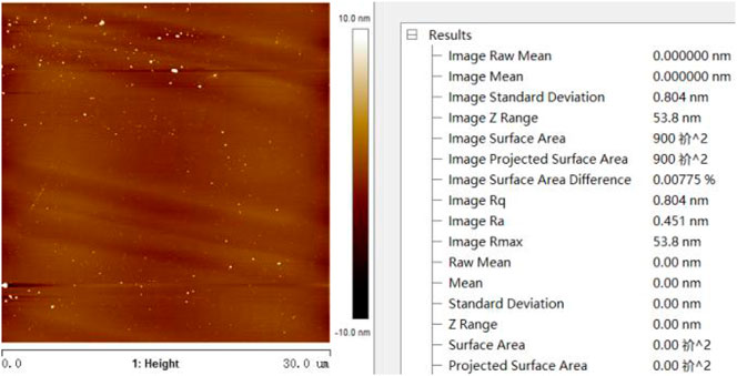
FIGURE 2. (Color online) AFM image of Ga2O3/SiO2 showing an RMS surface roughness of 0.54 nm within the area of 5 × 5 μm2.
In order to investigate the UV photoresponse of the β-Ga2O3 detector, the interdigital electrode was deposited by magnetron sputtering on the β-Ga2O3 film. The light sources with the wavelengths of 365 and 254 nm were gained from the UV lamps, respectively. The room-temperature I–V characteristics of the β-Ga2O3 PD in linear and logarithmic coordinates under dark conditions and 365-nm (1,200 μW/cm2) and 254-nm (300 μW/cm2) light illumination are shown in Figures 3A,B.
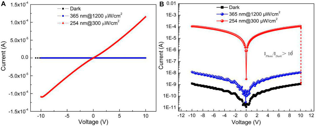
FIGURE 3. (Color online) I–V characteristic curves of the β-Ga2O3 PD in (A) linear and (B) logarithmic coordinates under dark conditions and 365 and 254-nm light illumination, respectively.
The I–V curves measured under dark conditions and 365-nm light do not show any obvious variations, and the currents remain ∼10–9 and ∼10–8 A at 10 V, respectively. With the applied voltage increasing, the current increases linearly both under dark and different illumination conditions (Figure 3A), suggesting an Ohmic contact between Ti/Au and β-Ga2O3 films. Similar results have been reported about the β-Ga2O3 thin film grown on Al2O3 with Ti/Au electrodes using laser molecular beam epitaxy technology (Guo et al., 2014a). Other than that, the current shows a sharp jump and increases constantly with the applied voltage intensity when the device is exposed under the 254-nm light (it is consistent with the bandgap ∼4.9 eV of β-Ga2O3). The photo-to-dark current ratio >105 was obtained at 10 V, suggesting that the photocurrent increases by five orders of magnitude under 254-nm light illumination. The low dark current is important for the practical PDs for it implies a high sensitivity and low noise for a superior device (Guo et al., 2014b). The results suggest that the β-Ga2O3 detector is not sensitive to 365-nm light, while it exhibits obvious photoresponse under 254-nm UV light illumination. Besides, the device will show typical MSM detector I–V properties when the gate voltage is not applied.
The back-gate structure β-Ga2O3 film detector was characterized under dark conditions by taking transport IDS-VGS (Figure 4A) and output Id-VDS (Figure 4B) tracings for different drain voltage (VDS) and gate voltage (VGS) values, respectively. Figure 4A shows that drain currents (IDS) appear when the VGS is greater than 20 V for different VDS, and IDS tends to become larger with the increase in VDS. The results suggest that the MOS transistor becomes on-state when VGS > 20 V and the IDS can be controlled by VGS; in other words, the typical three-terminal MOS structure fin field transistor (FET) can enhance the sensitiveness and responsivity with photoelectron regulation by adjusting the drain voltage and gate voltage. The on-state behavior of the current may also indicate the existence of weak contact resistance, which can also be surmised from the nonlinear output characteristics Id-VDS at very low VDS, as shown in Figure 4B. That is to say, the contact between Ti/Au and the β-Ga2O3 film still needs to be optimized. The same inference has been made on the back-gate a-MoS2 thin film transistors (Kouvatsos et al., 2015).
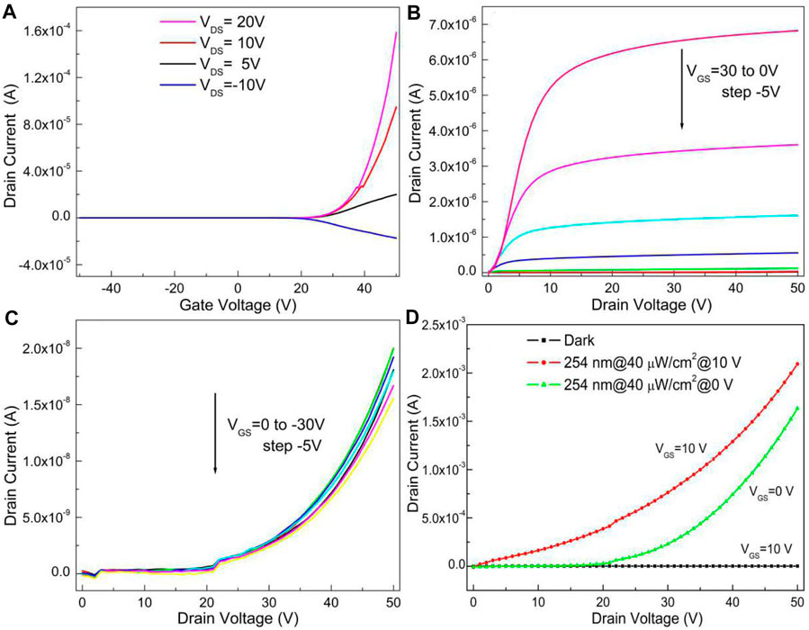
FIGURE 4. (Color online) (A) Transfer characteristics IDS-VGS of the back-gate structure based on the β-Ga2O3 film for various drain voltages. Output characteristics under dark conditions for gate voltages (B) from 30 to 0 V and (C) from 0 to −30 V, respectively. (D) Output characteristics for VGS = 10 V under dark conditions and VGS = 0 V and 10 V under 254-nm light illumination with a light intensity of 40 μW/cm2.
The output characteristics Id-VDS exhibit the dark currents (Id) that are closely related to VGS. With the VGS changed from 30 to 0 V (the step is −5 V) as shown in Figure 4B, Id is reduced by two orders of magnitude. This behavior indicates that VGS has a certain ability to regulate the dark current Id (under dark conditions). Along with the further decrease of VGS to −30 V (Figure 4C), Id almost tends to constant, that is, the regulation of VGS reaching saturation. The results exhibit typical Schottky barrier characteristics.
Figure 4D shows the characteristics of Ip-VDS under dark and 254-nm light illumination with a light intensity of 40 μW/cm2. Under the dark condition, the current–voltage characteristic showed good rectifying properties, and the rectification ratio reached 104 at VDS = ±10 V (Figures 4B,C). When the 254-nm light illuminated toward the PD, the generation of photocurrent (Ip) was clearly observed and increases rapidly vs. the drain voltage. What is more, Ip is affected by the gate voltage VGS, suggesting that VGS has a certain ability to regulate the photocurrent Ip regardless of the irradiation intensity. This indicates that this PD works properly as a Schottky barrier phototransistor. Similar three-terminal PDs have been constructed on MgZnO/ZnO/MgZnO/Si, which showed the same modulation (Ye et al., 2016). Furthermore, we find that Ip is proportional to the light intensity when the device is exposed to different light powers (the result is not shown here), that is to say, the device performance is affected by the tested light intensity, as reported on the similar PDs (Feng et al., 2018).
The time-dependent photoresponse of the β-Ga2O3 PD was measured to characterize the response speed using 254-nm light illumination under a fixed grain voltage VGS = 10 V for various drain voltages, as shown in Figure 5A. The measurements show that the detector still exhibits an identical response after several illumination cycles, indicating that the present device has excellent stability and good reversibility.
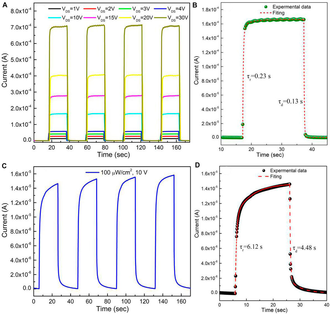
FIGURE 5. (Color online) (A) Time-dependent photoresponse of the β-Ga2O3 PD under a grain voltage VGS = 10 V for VDS = 1, 2, 3, 4, 10, 15, 20, and 30 V, respectively. (B) Experimental curve and fitted curve of the rise and decay processes of the device for VDS = 10 V. (C) Time-dependent photoresponse of the MSM structure PD without gate voltage. (D) Experimental curve and fitted curve of the rise and decay processes of the MSM structure device.
From the measurements at different VDS, one can see that the photocurrents rise and fall very rapidly and are obviously affected by VDS. Under 254-nm light illumination, the photocurrent instantaneously increases to a stable value of 7.1 × 10⁻⁴ A (VDS = 30 V), and it rapidly decreases to ∼10–8 A when the light turns off; the latter is quite close to the initial dark current value.
Compared with the Al2O3/β-Ga2O3 UV light PD (Sooyeoun et al., 2015; Wang et al., 2018) and other technological β-Ga2O3 PDs (Guo et al., 2014a; Xu et al., 2018; Tang et al., 2020) which show obvious relaxation phenomena, the present MOS structure device greatly reduces the rise and fall times, improving the sensitivity of the PD. For a more detailed study of the response time, the quantitative analysis of the current during the rise and decay processes involves the fitting of the photoresponse curve with an exponential relaxation equation of the following type (Ramana et al., 2014; Wang et al., 2018):
where I0 is the steady-state photocurrent, t is the time, A is a constant, and τ is the relaxation time constant. The enlarged view of the rise/decay processes and the corresponding fitting curves are shown in Figure 5B, and τr and τd denote the rise and decay time constants, respectively. The current of the rise process is steeper with τr = 0.23 ± 0.02 s and that of the decay process is τd = 0.13 ± 0.02 s, which implies that there are fewer oxygen vacancies or other defects (Feng et al., 2018). The present time constants are comparable to the available Ga2O3 PDs as listed in the study by Dong et al. (2019), although we remain skeptical of the fitted results of 0.03/0.08 s. Obviously, the present MOS structure device exhibited excellent responsivity compared with the MSM structure, as the results show in Figures 5C,D.
The spectral responsivity (R) is a critical parameter to evaluate the sensitivity of the PDs. According to the definition, the value of R is equal to the photocurrent generated by
where h is the Plank constant, c is the velocity of light, e is the electronic charge, λ is the wavelength of light, and Γ is the internal gain. For the present work, the value of
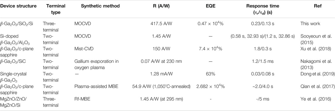
TABLE 1. Comparison on device performance of the present device and other PDs.
To better understand the mechanism of electron transfer on the MSM and back-gate MOS structure PD under the dark and light conditions, the schematic energy band diagrams are displayed in Figure 6. The Ti/Au contributes to a small MS interface barrier of 0.33 eV with close work function, suggesting approximate Ohmic contacts. For the Ohmic contact PD, the current path is directly formed while seldom affected by MS contact resistance, so that the material’s natural photoelectric performance can be better reflected.
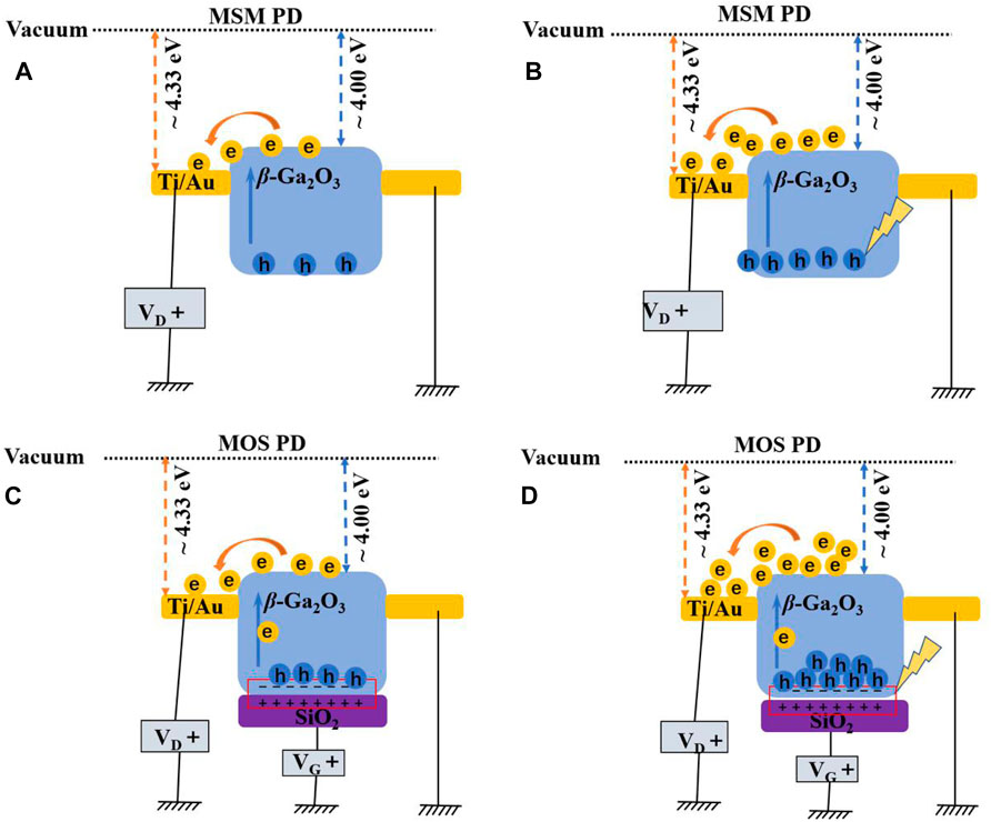
FIGURE 6. (Color online) The schematic energy band diagram for the (A) Ti/β-Ga2O3/Ti structured MSM PDs under dark conditions, (B) Ti/β-Ga2O3/Ti structured MSM PDs under illumination, (C) back-gate MOS structure PDs under dark conditions, and (D) back-gate MOS structure PDs under illumination.
As shown in Figure 6A, the dark currents remain at a low value with few separated hole–electron pairs, suggesting that the β-Ga2O3 film has few intrinsic defects. Under the 254-nm illumination, the photo-generated electrons jump to the valence band (VB) from the conduction band (CB) and gather on the β-Ga2O3 film surface, where electrons will transport under forward voltage, as shown in Figure 6B. By contrast, the MOS structure has a strong switching regulation effect on the channel layer to collect or deplete electrons; therefore, it exhibits boost forward current and low dark leakage current, compared with the MSM PD of the same size. For the three-terminal MOS structure, the SiO2 layer has strong dielectric properties that can effectively stop the electrons and holes from transporting across the SiO2/β-Ga2O3 interface and then dramatically reduce the vertical leakage loss and more effectively control the lateral movement of electrons in the β-Ga2O3 channel layer. This is a typical advantage of the MOS structure PD in regulating responsitivity and sensitivity over the MSM structure. When forward voltage was forced onto the SiO2 dielectric layer, the SiO2/β-Ga2O3 layer would induce a change in electric potential under the external electric field, as shown in Figure 6C and Figure 6D. It is obvious that a top-down high electric field has formed in the β-Ga2O3 film and varies with the external electric field, so that more electrons will obtain more kinetic energies and then jump into the VB. Eventually, more electrons will gather on the channel, which will form a directional movement current under forward drain bias voltage. Under 254-nm irradiation, a large number of photo-generated electrons rapidly accumulated in the channel layer under the action of the electric field from the β-Ga2O3 film. This is why the MOS structure PD displayed much weaker relaxation phenomena and much shorter rise and fall photoresponse times.
In this case, the composition of the channel electrons consists of photo-generated electrons, intrinsic electrons, and electric field–generated electrons; therefore, the MOS structure possesses enhanced responsivity compared with the MSM structure. On the contrary, if the gate is forced on reverse bias, an opposite internal electric field will be generated onto the β-Ga2O3 film and it gradually depletes the channel electrons, presenting a low leakage current. In general, the advantages of the back-gate MOS structure PD are as follows: for one thing, it keeps the design of the top interface on the MSM structure, ensuring the photosensitive area is sufficiently exposed to illumination; for another, the back-gate structure is made at the bottom, realizing the responsive regulation and reducing the relaxation phenomena.
In conclusion, the solar-blind PD with the back-gate MOS structure was fabricated on the β-Ga2O3 film, which exhibited obvious photoresponse under 254-nm UV light illumination, and the photocurrent could be controlled by VGS. Otherwise, the dark current could also be regulated by VGS and tended to constant when the regulation of VGS was reaching saturation. What is more, VGS had a certain ability to regulate the photocurrent. The present device demonstrated excellent stability and fast response (rise) and recovery (decay) times under the 254-nm light illumination. All these excellent characteristics indicate that the back-gate MOS structure β-Ga2O3 film has great potential applications on the solar-blind UV PDs.
The raw data supporting the conclusions of this article will be made available by the authors, without undue reservation.
XJ fabricated the material and characterized the detector. DM analyzed the experimental results. All authors contributed to the writing of the article and evaluation of the results.
This work is supported by the Shandong Provincial Natural Science Fund (ZR2019BA025) and partially supported by the Project funded by the China Postdoctoral Science Foundation (042600055) and Research on Frontiers of Materials Science, the Beijing Municipal Science and Technology Commission (Z181100004418006).
The authors declare that the research was conducted in the absence of any commercial or financial relationships that could be construed as a potential conflict of interest.
Alaie, Z., Nejad, S. M., and Yousefi, M. H. (2015). Recent Advances in Ultraviolet Photodetectors. Mater. Sci. Semicond. Process. 29, 16–55. doi:10.1016/j.mssp.2014.02.054
Dong, L. P., Yu, J. G., Jia, R. X., Hu, J. C., Zhang, Y. M., and Sun, J. W. (2019). Self-powered MSM Deep-Ultraviolet β-Ga2O3 Photodetector Realized by an Asymmetrical Pair of Schottky Contacts. Opt. Mater. Exp. 9, 1191–1199. doi:10.1364/OME.9.001191
Feng, Z. Q., Huang, L., Feng, Q., Li, X., Zhang, H., Tang, W. H., et al. (2018). Influence of Annealing Atmosphere on the Performance of a β-Ga2O3 Thin Film and Photodetector. Opt. Mater. Exp. 8, 2229–2237. doi:10.1364/OME.8.002229
Guo, D. Y., Wu, Z. P., An, Y. H., Guo, X. C., Chu, X. L., Sun, C. L., et al. (2014b). Oxygen Vacancy Tuned Ohmic-Schottky Conversion for Enhanced Performance in β-Ga2O3Solar-Blind Ultraviolet Photodetectors. Appl. Phys. Lett. 105, 023507. doi:10.1063/1.4890524
Guo, D. Y., Wu, Z. P., Li, P. G., An, Y. H., Liu, H., Guo, X. C., et al. (2014a). Fabrication of β-Ga2O3 Thin Films and Solar-Blind Photodetectors by Laser MBE Technology. Opt. Mater. Exp. 4, 1067–1076. doi:10.1364/OME.4.001067
Hu, G. C., Shan, C. X., Zhang, N., Jiang, M. M., Wang, S. P., and Shen, D. Z. (2015). High Gain Ga2O3 Solar-Blind Photodetectors Realized via a Carrier Multiplication Process. Opt. Exp. 23, 13554–13561. doi:10.1364/OE.23.013554
Kokubun, Y., Miura, K., Endo, F., and Nakagomi, S. (2007). Sol-gel Prepared β-Ga2O3 Thin Films for Ultraviolet Photodetectors. Appl. Phys. Lett. 90, 031912. doi:10.1063/1.2432946
Kouvatsos, D. N., Papadimitropoulos, G., Spiliotis, T., Vasilopoulou, M., Barreca, D., Gasparotto, A., et al. (2015). Electrical Characteristics of Vapor Deposited Amorphous MoS2 Two‐terminal Structures and Back Gate Thin Film Transistors with Al, Au, Cu and Ni‐Au Contacts. Phys. Status Solidi C. 12, 975–979. doi:10.1002/pssc.201510025
Monroy, E., Omnes, F., and Calle, F. (2003). Wide-bandgap Semiconductor Ultraviolet Photodetectors. Semicond. Sci. Tech. 18, R33–R51. doi:10.1088/0268-1242/18/4/201
Nakagomi, S., Momo, T., Takahashi, S., and Kokubun, Y. (2013). Deep Ultraviolet Photodiodes Based on β-Ga2O3/SiC Heterojunction. Appl. Phys. Lett. 103, 072105. doi:10.1063/1.4818620
Oshima, T., Okuno, T., Arai, N., Suzuki, N., Ohira, S., and Fujita, S. (2008). Vertical Solar-Blind Deep-Ultraviolet Schottky Photodetectors Based on β-Ga2O3 Substrates. Appl. Phys. Exp. 1, 011202. doi:10.1143/APEX.1.011202
Qian, L. X., Zhang, H. F., Lai, P. T., Wu, Z. H., and Liu, X. Z. (2017). High-sensitivity β-Ga2O3 Solar-Blind Photodetector on High-Temperature Pretreated C-Plane Sapphire Substrate. Opt. Mater. Exp. 7, 3643. doi:10.1364/OME.7.003643
Ramana, C. V., Rubio, E. J., Barraza, C. D., Gallardo, A. M., McPeak, S., Kotru, S., et al. (2014). Chemical Bonding, Optical Constants, and Electrical Resistivity of Sputter-Deposited Gallium Oxide Thin Films. J. Appl. Phys. 115, 043508. doi:10.1063/1.4862186
Sooyeoun, O., Jung, Y., Michael, A. M., Jennifer, K. H., Charles, R. E., and Kim, J. (2015). Development of Solar-Blind Photodetectors Based on Si-Implanted β-Ga2O3. Opt. Exp. 23, 028300. doi:10.1364/OE.23.028300
Suzuki, R., Nakagomi, S., Kokubun, Y., Arai, N., and Ohira, S. (2009). Enhancement of Responsivity in Solar-Blind β-Ga2O3 Photodiodes with a Au Schottky Contact Fabricated on Single crystal Substrates by Annealing. Appl. Phys. Lett. 94, 222102. doi:10.1063/1.3147197
Suzuki, R., Nakagomi, S., and Kokubun, Y. (2011). Solar-blind Photodiodes Composed of a Au Schottky Contact and a β-Ga2O3 Single crystal with a High Resistivity Cap Layer. Appl. Phys. Lett. 98, 131114. doi:10.1063/1.3574911
Tang, R. F., Li, G. Q., Li, C., Li, J. C., Zhang, Y. F., Huang, K., et al. (2020). Localized Surface Plasmon Enhanced Ga2O3 Solar Blind Photodetectors. Opt. Exp. 28, 5731–5740. doi:10.1364/OE.380017
Wang, X., Chen, Z. W., Guo, D. Y., Zhang, X., Wu, Z. P., Li, P. G., et al. (2018). Optimizing the Performance of a β-Ga2O3 Solar-Blind UV Photodetector by Compromising between Photoabsorption and Electric Field Distribution. Opt. Mater. Exp. 8, 2918–2927. doi:10.1364/OME.8.002918
Xu, Y., An, Z. Y., Zhang, L. X., Feng, Q., Zhan, J. C., Zhang, C. F., et al. (2018). Solar Blind Deep Ultraviolet β-Ga2O3 Photodetectors Grown on Sapphire by the Mist-CVD Method. Opt. Mater. Exp. 8, 2941–2947. doi:10.1364/OME.8.002941
Keywords: Ga2O3 film, solar-blind photodetector, back-gate MOS structure, photocurrent, responsivity
Citation: Meng DD, Ji XQ, Wang DF and Chen ZW (2021) Enhancement of Responsivity in Solar-Blind UV Detector With Back-Gate MOS Structure Fabricated on β-Ga2O3 Films. Front. Mater. 8:672128. doi: 10.3389/fmats.2021.672128
Received: 25 February 2021; Accepted: 01 June 2021;
Published: 18 June 2021.
Edited by:
Harry E. Ruda, University of Toronto, CanadaReviewed by:
Yongqiang Yu, Hefei University of Technology, ChinaCopyright © 2021 Meng, Ji, Wang and Chen. This is an open-access article distributed under the terms of the Creative Commons Attribution License (CC BY). The use, distribution or reproduction in other forums is permitted, provided the original author(s) and the copyright owner(s) are credited and that the original publication in this journal is cited, in accordance with accepted academic practice. No use, distribution or reproduction is permitted which does not comply with these terms.
*Correspondence: Zhengwei W. Chen, emhlbmd3ZWljaGVuQGJ1cHQuZWR1LmNu
†These authors have contributed equally to this work and share first authorship
Disclaimer: All claims expressed in this article are solely those of the authors and do not necessarily represent those of their affiliated organizations, or those of the publisher, the editors and the reviewers. Any product that may be evaluated in this article or claim that may be made by its manufacturer is not guaranteed or endorsed by the publisher.
Research integrity at Frontiers
Learn more about the work of our research integrity team to safeguard the quality of each article we publish.