- School of Electrical Engineering, Vellore Institute of Technology, Vellore, India
Research has focused on multilevel inverters (MLIs) due to their use in electric vehicles, renewable energy systems, and industrial applications. This paper proposes a new design for a single-phase 21-level asymmetrical MLI for photovoltaic (PV) applications that reduces the number of components, voltage stress, and overall size and cost. Enhanced incremental maximum power point tracking (EINC-MPPT) is used in the PV standalone system to offer a fast dynamic response, track maximum power, and regulate the PV module output voltage. This paper presents a PV-boost DC–DC single-input multi-output (SIMO) converter linked to solar panels to provide supply voltage to the inverter. A level-shifted constant multicarrier sinusoidal pulse width modulation (LSCMSPWM) technique is used to produce a better-synthesized output waveform from the MLI, resulting in low total harmonic distortion (THD) and also meeting IEEE standards. The suggested MLI is simulated in MATLAB/Simulink and tested with a hardware prototype under various load conditions. It is suitable for medium-power and grid-connected renewable energy systems applications. The qualitative and quantitative parameters of the proposed MLI have been evaluated by cost function (CF), number of components, reliability, THD, and total standing voltage (TSV); these parameters are compared with the existing MLIs.
1 Introduction
1.1 Background and motivation
Renewable energy sources are becoming more popular. Environmental consciousness and global energy use are increasing. In contrast, natural resources such as gas, coal, and oil are finite and rapidly depleting (Das et al., 2024). Given the limited availability of these resources, it is now necessary to explore alternative energy sources (Rahimi et al., 2023). Surprisingly, the extensive use of solar energy is leading to growing concerns about the quality, dependability, and coordination of the power grid (Tayyab et al., 2023). To ensure the safe and reliable use of photovoltaic (PV) energy, various countries have established different grid codes (Nyamathulla and Chittathuru, 2023). MLIs are increasingly using PV systems as their primary energy source (Ali Khan et al., 2020). Multilevel inverters (MLIs) have become more common due to their many advantages, such as high power operating capacity, reduced switching losses, outstanding power quality, and low harmonics (Tayyab et al., 2022). These MLIs use several DC sources and power semiconductor switches to produce stepping voltage waveform. Raising their level could improve this voltage waveform (Chappa et al., 2021). It is difficult to achieve MLI reliability and efficiency because of the increased cost and component count of circuits. Three of the most common MLI structures are a neutral point clamped (NPC), a flying capacitor (FC), and a cascaded H-bridge (CHB) (Alhassane Soumana et al., 2022).
1.2 Literature review
According to Omer Prabhu et al. (2020a), CHB MLI provides two different single-phase H-bridge topologies—symmetrical and asymmetrical—that are dependent on DC voltage. In contrast to symmetrical MLIs, asymmetrical ones use DC voltage sources of varying magnitudes. A standard CHB-type inverter will often have a positive, zero, or negative output (Prasad and Dhanamjayulu, 2022). Rao et al. (2018) suggested assessing the output of CHB-type inverters by aggregating the output voltages of each unit. Recently developed control methods suggest CHB inverter topologies, but the full-bridge converter changes DC step outputs into AC. The limited use of full-bridge converters stems from their inability to block higher voltages, while innovative topologies can reduce both single- and three-phase system components (Majeed Shaikh et al., 2023). Some topologies used modular MLIs to provide multilevel outputs with fewer switching devices and DC sources. These topologies use antiparallel bidirectional switches to transfer current in either direction, with minimal switching components (Kumar et al., 2022). Since cascaded subunits reduce switching-device blocking voltage, they resemble modules. The problem with such topologies is that the output level increases the number of switching devices (Sinha et al., 2018). Novel MLI designs are required to provide reduced blocking voltage, more output levels, and fewer components (Bana et al., 2019). This can reduce inverter size and price. Recent work has included a stacked H-bridge MLI architecture with basic units on each side of the complete bridge (Shaik and Dhanamjayulu, 2021).
According to Das et al. (2020), researchers have been studying cascaded MLI topology configurations. There is a singular symmetric MLI that requires fewer switches. An evolutionary algorithm creates a new design and a proven way of controlling both resistive and motor loads, keeping the output voltage stable even when loads change. Babaei et al. (2014) introduced a transistor-clamped H-bridge MLI design by enabling the various output levels for higher voltage and power ratings without necessitating an increase in component ratings. Carrier-based PWM efficiently controls the MLI, which has fewer switching losses at high switching frequencies (Siddique et al., 2020). High-frequency switching applications incur power losses. However, the topologies discussed in Omer et al. (2020b), Das et al. (2018), Sabyasachi et al. (2020), and Sarwer et al. (2020) address the challenges of more components, bulky circuits, high control complexity, THD, and low efficiency. The next step is to categorize standalone inverters as either symmetrical or asymmetrical (Prasad et al., 2021). Using the same value for each DC source indicates a symmetrical arrangement, while using different values for the DC sources results in an asymmetrical design. Meraj et al. (2020) presents two configurations ideal for low- and medium-rated solar power generation. According to Samadaei et al. (2016), FC and NPC MLIs struggle with voltage balance.
MLIs are increasingly used with PV systems as their primary energy source, and a segregated MLI architecture is best for PV integration (Alishah et al., 2017). These systems are highly efficient at electricity generation and have the added benefit of being environmentally friendly (Samadaei et al., 2018). The production of solar PV can be influenced by variations in temperature and solar radiation over time (Narendra Babu, 2024). A PV system’s efficient operation heavily relies on implementing MPPT techniques. Numerous advanced MPPT techniques have been developed to improve the performance of PV systems (Alishah et al., 2016). DC–DC converters effectively handle duty cycle fluctuation to optimize power in MPPT systems. MPPT methods such as hill climbing (HC) and perturbing and observing (P&O) are commonly used due to their straightforwardness (Shaik et al., 2023). Choosing the best MPPT methodology for an application can be challenging because each approach has its advantages and disadvantages. The HC and P&O algorithms are unable to achieve global maximum partial probability (GMPP) in partial shadow (Akbari et al., 2022).
1.3 Challenges
Two-level voltage source inverters are not ideal for greater power applications due to their inability to handle high voltages and the increased electromagnetic interference caused by higher dv/dt (Krishnachaitanya and Chitra, 2021). It is necessary to address these issues to overcome these limitations. MLIs are the best option, offering advantages such as reduced voltage step, improved power quality, less switching losses, minimal harmonics, and improved electromagnetic compatibility (Mustafa et al., 2022). Additionally, as the voltage level rises in diode-clamped MLI systems, capacitor voltage balancing becomes challenging, limiting them to three levels. The utilization of FC-MLIs necessitates an increased number of DC capacitors to accommodate increased voltage levels (Hosseinzadeh et al., 2021). Nevertheless, it is possible to adjust the switching combinations and achieve balanced DC capacitor voltage (Siddique et al., 2019). CHB MLI architecture has gained in popularity and reliability because of its modularity. Nevertheless, every bridge needs a separate DC power supply. Additionally, as the levels grow, there is a greater demand for switches (Thakre et al., 2019). Topologies have been proposed as a cost-effective solution to address power quality concerns and meet high grid-code criteria (Montazer et al., 2021). These topologies are mostly derived from conventional ones; novel optimal MLI designs are required to provide high reliability, low THD, reduced blocking voltage, more output levels, and fewer components. This can reduce inverter size and price.
1.4 Contributions
Some of the most important contributions of this study are:
a. The design of a standalone solar PV system integrated with a PV boost DC–DC SIMO converter and a 21-level MLI architecture that minimizes the number of components and reduces voltage stress, total size, and cost.
b. An EINC-MPPT is used in the PV standalone system to offer a fast dynamic response, track maximum power, and regulate the PV module output voltage.
c. The LSCMSPWM approach delivers a better-synthesized output waveform from the MLI, and the resulting THD of 2.26% also fulfills IEEE standards.
d. The suggested MLI is appropriate for medium-power and grid-connected renewable energy systems applications.
e. The qualitative and quantitative parameters of the proposed 21-level MLI outperform conventional topologies.
1.5 Structure
This study is arranged as follows. The standalone solar PV system and DC–DC boost SIMO converter are presented in Section 1. Section 2 provides a detailed explanation of the suggested 21-level MLI topology operation. In Section 3, both simulation and hardware validation results are presented. Section 4 evaluates and compares the performance parameters of various MLI topologies with the proposed MLI. Finally, Section 5 covers conclusions and future scope.
2 Proposed system
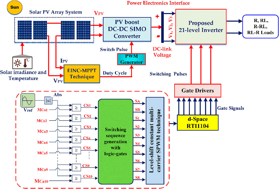
The proposed system’s overall block diagram consists of a solar PV system and a PV boost DC–DC SIMO converter with a proposed MLI (Figure 1). PV technology converts light energy into electrical energy, and solar PV can modify its power production in response to changes in weather conditions and temperature. The suggested method uses a three-level converter with the EINC-MPPT technique to send DC power from PV cells to the proposed MLI architecture. The inverter collects the power that the PV panels generate. A driver circuit will activate switches as needed, employing logic circuits to produce switching pulse patterns via sequence generators. Ultimately, the proposed MLI will provide the load with 21-level output.
2.1 Design of the solar PV system
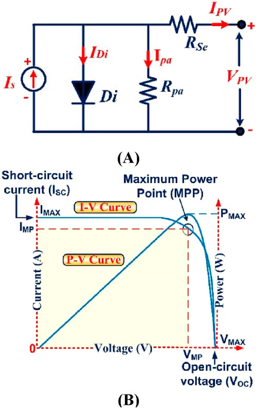
The proposed standalone solar PV system includes a selected solar panel, the 1Soltech 1STH-215-P, which has six series and two parallel units per string. Figures 2A, B display the equivalent circuit of the solar PV cell and the characteristics of the solar PV panel. Di is the diode, RPa, RSe are the resistances of parallel and series resistances, and npa, nse are the number of parallel and series connected cells, respectively.
From the ideal PV circuit, the diode current can be calculated using Equation 1:
where
Panel Output power can be calculated by using Equation 2:
By applying KCL to the PV cell equivalent circuit,
Therefore solar PV output current can be calculated by using Equations 3, 4:
The short circuit current (IS) and irradiance intensity can be calculated using Equations 5, 6:
where the temperature coefficient is β, reference temperature is TR, and short circuit current IS(TR) values are included in the PV data sheets.
Therefore, the irradiance intensity is
where Gn indicates normal irradiation value.
The saturation current (I0) can be calculated by Equation 7:
2.2 PV boost DC–DC SIMO converter with the EINC-MPPT technique
Figures 3A, B show the connection of a PV boost DC–DC SIMO converter to solar PV panels with EINC-MPPT and solar PV-integrated with PV boost DC–DC SIMO converter for the proposed MLI. This converter consists of switches (SB, SL), three DC-link capacitors (C1, C2, C3), and a boost inductor (L) to bring the output voltage of the PV system up to a satisfactory level for the inverter input (Rao et al., 2018). The boost converter employs an EINC-MPPT algorithm to automatically track the MPP of the PV array. The following subsections provide a comprehensive explanation of several aspects of the suggested technique.
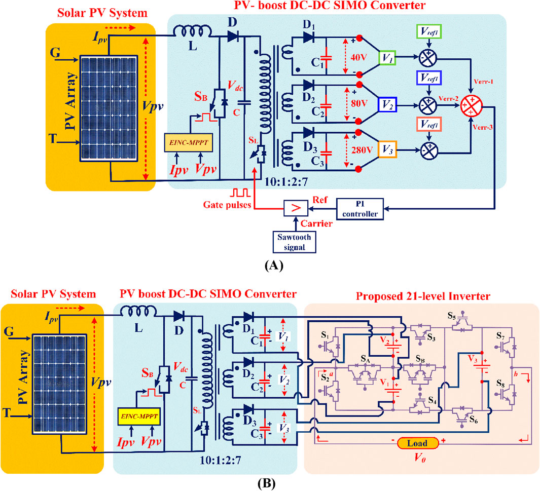
Figure 3. (A) EINC-MPPT controlled PV boost DC–DC closed loop SIMO converter. (B) Solar PV integrated with the PV boost DC–DC SIMO converter for proposed MLI.
When switch SB is on, the output state is isolated, and an inductor (L) and a switch (S) are used to transfer the increasing input current (IPV). The solar PV output voltage (VPV) powers the inductor while the switch is on (Ton).
Therefore the inductor voltage can be calculated using Equation 8:
When switch SB is off (Toff), current from the inductor is forced to flow through the load and diode (D). This diode can load the inductor (L) from the voltage source.
Therefore the output voltage of converter is VBdc and can be calculated Equation 9:
The boost converter output voltage is controlled by the duty cycle (δ) of the control switch. By altering the switch’s on-time, the output voltage can be precisely controlled.
Therefore, the DC–DC boost converter output voltage can be calculated by Equation 10:
where δ =
The inductor and capacitor ratings are calculated using Equations 11, 12:
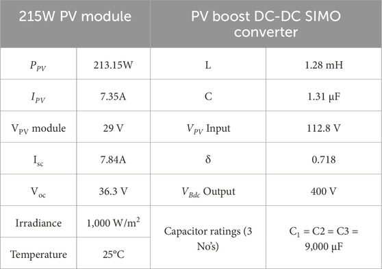
where ΔIL is the input current, ΔVBdc is the output voltage ripple factors, and fs is the switching frequency. To obtain a reasonable estimate of the values of the inductor and capacitor, it is recommended limiting ΔIL to 30% and generally assuming ΔVBdc at 5%. The characteristics of the solar PV module DC–DC boost converter requirements are detailed in Table 1.
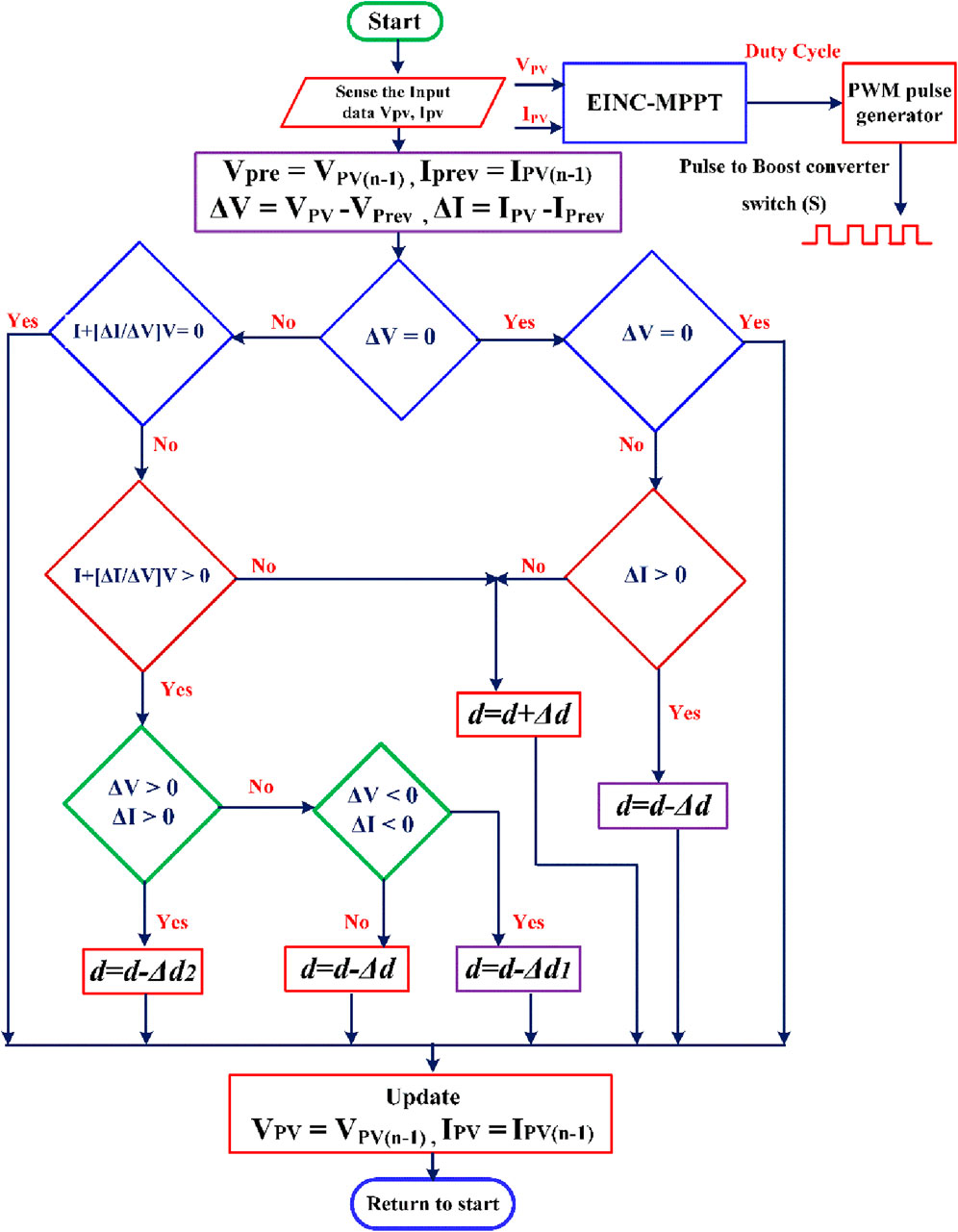
The MPPT controller controls the performance of the boost converter by considering inputs such as temperature, solar radiation, PV array (Voc and Isc) characteristics, and DC link voltage. When the operating point varies around the maximum power point (MPP), especially in situations with rapidly changing irradiance levels, the effectiveness of conventional incremental and conductance MPPT algorithms decreases. To address these problems, an EINC-MPPT technique is implemented; Figure 4 illustrates a flowchart of an EINC-MPPT technique.
2.3 Proposed 21-level asymmetrical MLI topology
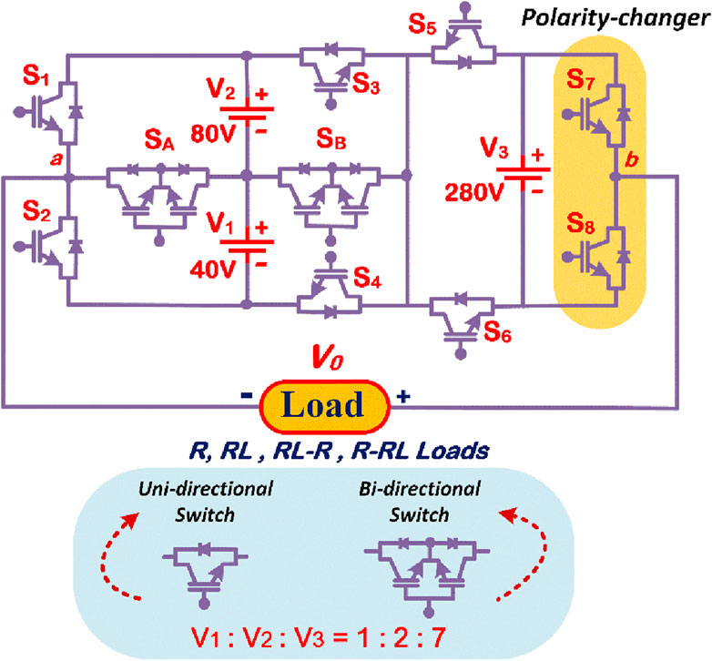
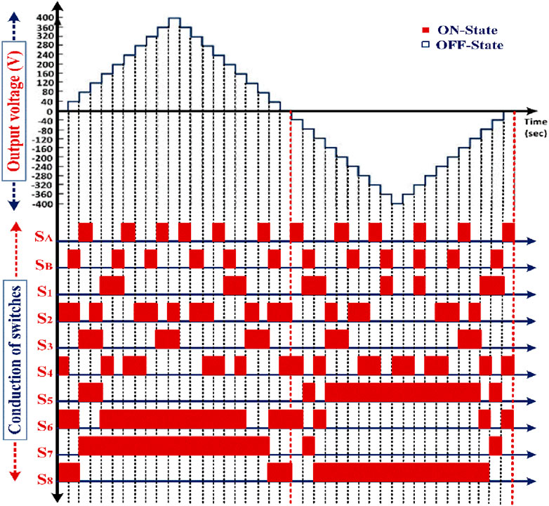
The proposed 21-level MLI architecture consists of fewer components without any inductors, capacitors, and diodes (Figure 5). It consists of only two bidirectional switches (SA and SB), eight unidirectional switches (S1, S2, S3, S4, S5, S6, S7, S8), and three asymmetrical voltage sources (V1, V2, V3) to achieve 21 voltage levels, with each voltage step Vdc = 40 V and the maximum output voltage 400 V. The DC voltage ratio is crucial for maximizing output voltage and reducing the inverter’s TSV. Based on the recommended MLI architecture, the required component estimations follow.
2.3.1 Components selection
For the proposed MLI asymmetric operation required DC voltage sources are represented below using Equation 13:
The required DC sources, switches, driver circuits, and maximum output voltage of the proposed MLI are determined using Equations 14–17, where NLev indicates the number of levels:
The maximum voltage output (Vo,max) is
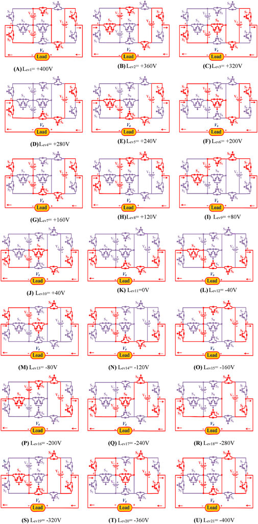
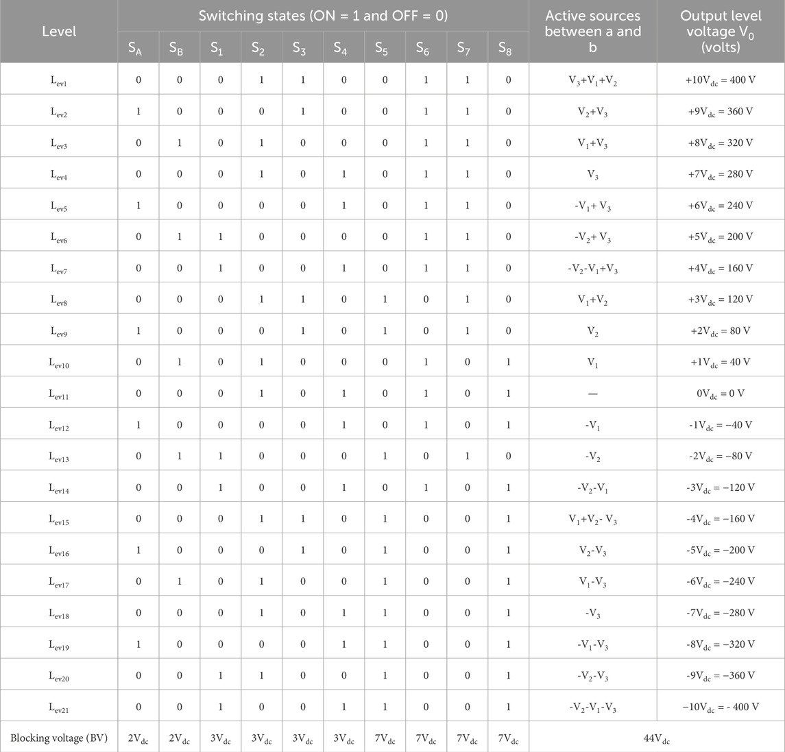
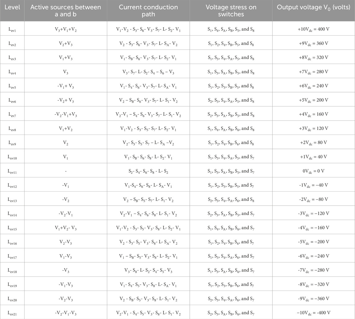
The switches are vital in producing 21 levels using the switching pattern generated by the switching pulse generators. The suggested operational modes of the MLI topology are shown in Figures 6A–U. The various output voltage levels and their corresponding switching states are detailed in Table 2. The current conduction paths are listed in Table 3, and the waveform of the predicted output voltage of the suggested MLI is displayed in Figure 7.
2.3.2 Level-shifted constant multicarrier sinusoidal pulse width modulation (LSCMSPWM) technique
The proposed MLI needs the right modulation methods to obtain a lower THD that meets the IEEE standard limits and provides good power from the MLI end. Modulation methods enhance the synthesis of the MLI output waveform. To provide gating signals for the power switching devices of the converter, the fundamental frequency is used. In this case, a pulse width modulation technique is used as a control. The optimal reference sinusoidal pulse is associated with level-shifted average level constant multicarrier signals of similar characteristics, which are used to generate gating signals for controlling power converter switches.
This control approach requires (NLev−1)/2 average level constant multicarrier signals to achieve the required output voltage levels. The modulation technique generates the model voltage output waveform and logic gate-based (LGB) switching gate pulse generators to store the switching order of every switching device (Figures 8A, B). Ten average-level constant multicarrier pulses (MCa1 – MCa10) can produce 21 voltage levels with different shift values but equal frequency. Gate pulse patterns for power converter switching devices are generated by comparing average level constant multicarrier carrier signals with a pure sinusoidal waveform signal (Vref = |Vm sin (ωt)|).
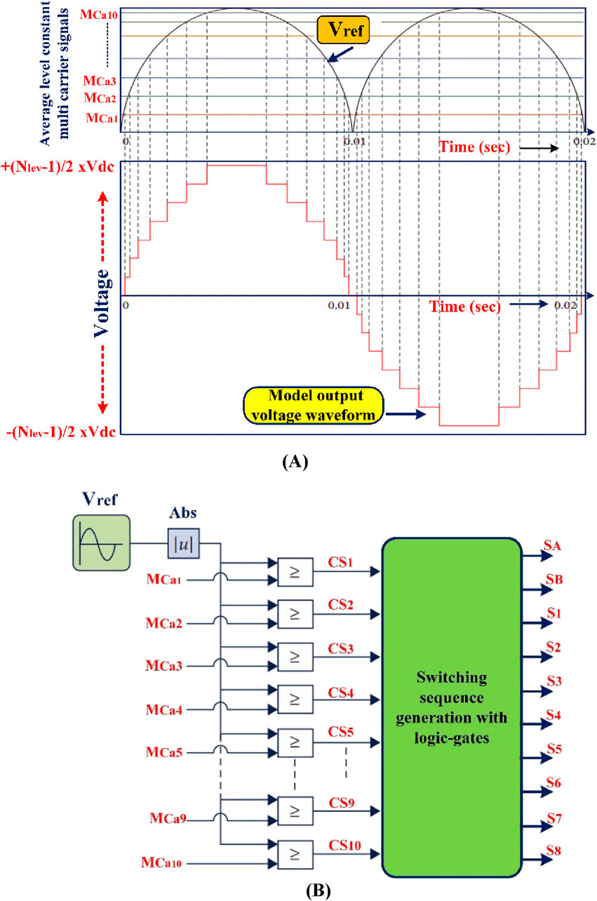
Figure 8. (A) Expected output voltage waveform of the LSCMSPWM technique. (B) LSCMSPWM technique switching sequence generation for proposed 21-level MLI.
The amplitude of the level-shift constant multicarrier pulse modulated index (Ma) is calculated using Equation 18:
The variables Vm and Vcr denote the peak voltage amplitude of the reference signal and the voltage of the constant multicarrier signals, respectively. The proposed 21-level MLI topology requires one fundamental sinusoidal waveform with a 50 Hz frequency as a reference and ten average-level constant multicarrier signals to generate the pulses for power switches. The RMS output voltage of the proposed MLI with its respective modulation index can be calculated using Equation 19:
The optimal output voltage waveform is clipped more frequently as the switching frequency increases. This limits its fluctuation to short intervals.
3 Result analysis
To observe the proposed MLI’s real-time response to various load conditions, it is necessary to simulate and validate the recommended MLI architecture by implementing the prototype. The subsequent sections detail the outcomes of both the simulation and experimental results.
3.1 Simulation results
The simulation results of the solar PV panel and PV-boost SIMO converter output voltages with EINC-MPPT are displayed in Figure 9A. The solar PV panel at MPP generates 112.8 V and is boosted to 400 V using a PV boost converter on the side of a SIMO converter. The PV boost DC–DC SIMO-converter simulated input and output voltages are displayed in Figure 9B. The DC link voltage response comparison for different MPPT techniques is displayed in Figure 9C. The proposed EINC MPPT technique is very effective, with a lower settlement time of 0.085 s than other MPPT techniques.
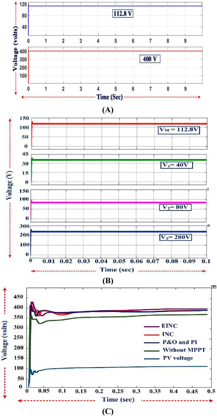
Figure 9. (A) Simulated output voltage of the solar PV panel and DC–DC boost converter on the side of the SIMO converter. (B) Simulated input and output voltages of the PV boost DC–DC SIMO converter. (C) DC-link voltage response with different MPPT algorithms.
The suggested MLI circuit is modeled and simulated using MATLAB/Simulink software. The switch pulse patterns are produced at a switching frequency of 5 kHz by comparing the multicarrier signals through a 50 Hz sinusoidal signal. The modeled topology is tested for R-load as well as RL-loads. The output voltage and current waveforms of the proposed MLI are shown in Figures 10A–C. These show the output voltage and current waveforms of the MLI with R = 200Ω load and the output voltage and current waveforms of the MLI with an RL-load (R = 200Ω, L = 200 mH), respectively. The simulated FFT analysis THD of 2.06% is displayed in Figure 10D.
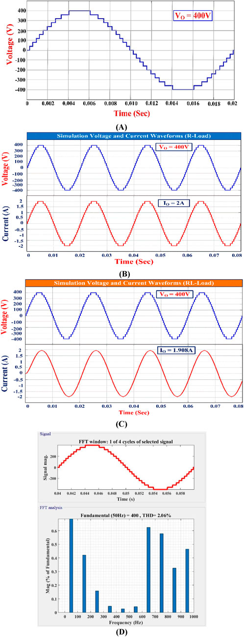
Figure 10. (A) Simulated output voltage of proposed 21-level MLI. (B) Simulated output voltage and current waveforms of proposed MLI for R-load. (C) Simulated output voltage and current waveforms of proposed MLI for RL-load. (D) Simulated THD of proposed 21-level MLI.
3.2 Hardware results
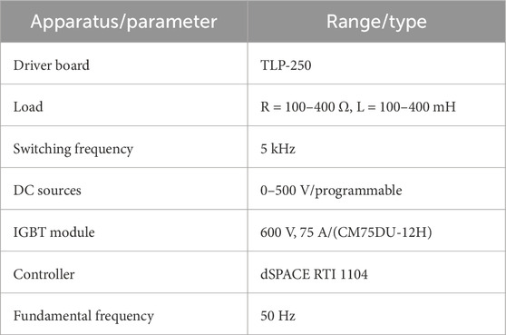
The experimental testing of the proposed MLI architecture was conducted, and the component specifications are listed in Table 4. Power-switching IGBT (CM75DU-12H) devices, optocouplers (MCT2E), and asymmetrical DC sources are used to implement this hardware prototype. The dSPACE RT1104 controller is used to generate the switching sequence for each switching device, using optocouplers for activation. The hardware prototype was tested with various load conditions, achieving a 21-level output voltage of 400 V. The voltage and current output waves were examined, and the results were captured using a DSO connected to the prototype via a differential probe. A hardware prototype of the suggested MLI is shown in Figure 11A.
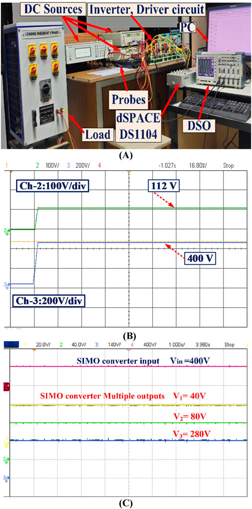
Figure 11. (A) Experimental setup of proposed 21-level MLI. (B) Experimental output voltage of the solar PV panel and PV-boost converter. (C) Experimental input and output voltages of the closed loop SIMO converter.
Figure 11B presents the experimental output voltage waveforms of the solar PV panel as well as the PV-boost converter. Figure 11C presents the input and output voltages of the PV-boost DC–DC SIMO converter.
Figures 12A–D present the output voltage as well as the voltage and current waveforms of a proposed MLI for R = 200Ω load and RL-load (R = 200Ω, L = 200 mH), as well as the output voltage waveform for various modulation index (Ma) values, respectively. Figures 13A–D present the output current behavior when the dynamic load changes from R- to RL-load. Figures 14A–E present the output current behavior when the dynamic load changes from RL- to R-. The output voltage THD is 2.26%—in line with IEEE standards.
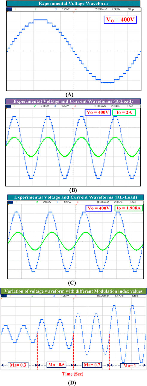
Figure 12. Proposed MLI experimental waveforms. (A) Output voltage waveform. (B) Output voltage and current waveforms for R-load. (C) Output voltage and current waveforms for RL-load. (D) Output voltage for different modulation index (Ma) values.
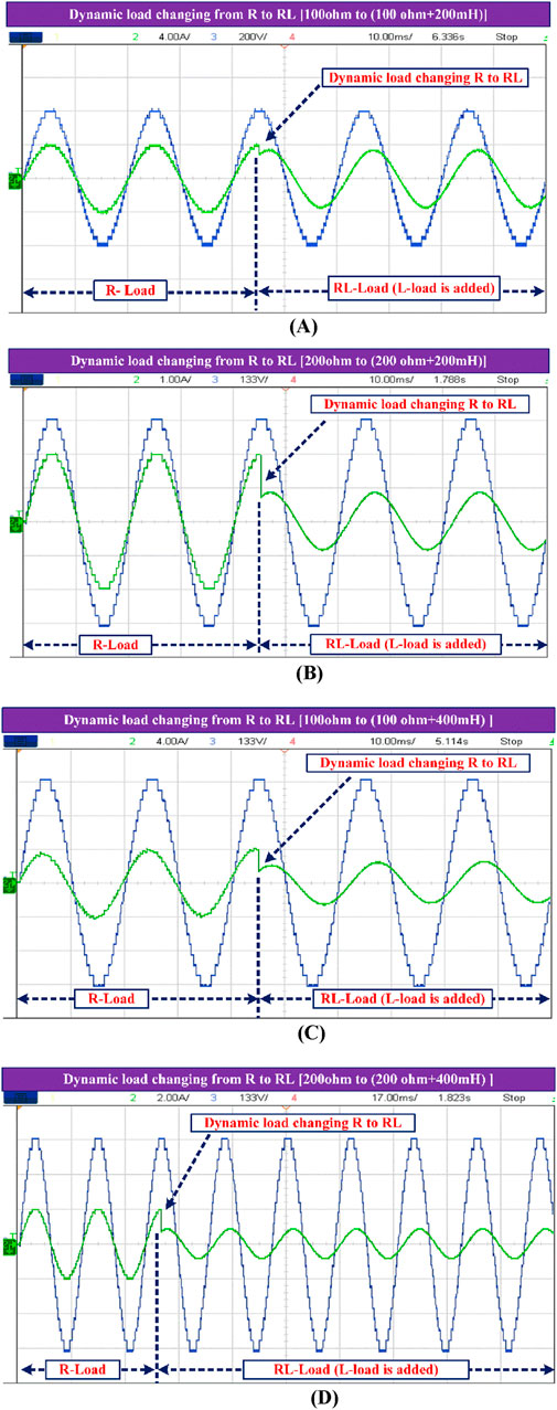
Figure 13. Experimental voltage and current waveforms for dynamic load changes from R- to RL-load. (A) 100 Ω to (100 Ω + 200 mH). (B) 200 Ω to (200 Ω + 200 mH). (C) 100 Ω to (100 Ω + 400 mH). (D) 200 Ω to (200 Ω + 400 mH).

Figure 14. Experimental voltage and current waveforms for dynamic load changes from RL- to R-load. (A) {100 Ω + 200 mH} to 100 Ω. (B) {200 Ω + 200 mH} to 200 Ω. (C) {100 Ω + 400 mH} to 100Ω. (D) {200 Ω + 400 mH} to 200Ω. (E) Experimental THD of suggested MLI.
4 Comparative analysis
The proposed 21-level MLI architecture was compared using performance indicators like TSV, THD, losses, efficiency and reliability parameters’ fault rate (FRT), and mean time to failure (MTTFT). Procedures and computations for these performance indicators are discussed below. Various qualitative and quantitative parameters are compared, tabulated, and graphically illustrated.
4.1 Total standing voltage (TSV) calculation
TSV is extensively used to choose power switches. All power-switching devices in the design have an influence on TSV (Prasad and Dhanamjayulu, 2022). To calculate the blocked voltage across power-switching devices, VSbi = Vi and VSuni = 2Vi are the voltage stresses on the bi- and uni-directional switches, respectively, where i = 1, 2, n and n is the power switch.
Therefore, the maximum output voltage is calculated using Equation 20:
The maximum blocking voltage (MBV) of particular switches can be calculated using Equations 21–23:
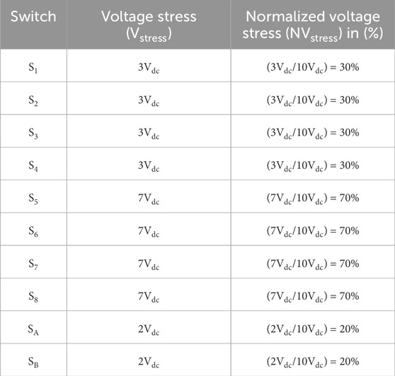
The normalized voltage stress (NVstress) is defined as the ratio of the switch’s Vstress to Vo,max. The Vstress is the true voltage stress. Respective switch voltage stress values are listed in Table 5.
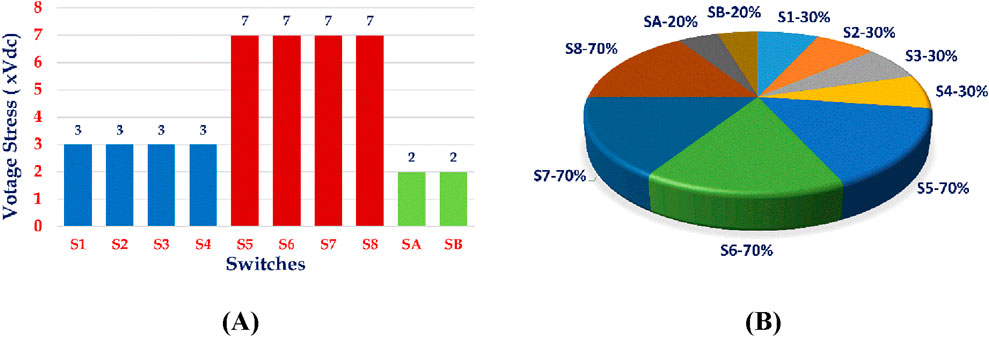
Figures 15A, B show each switch voltage stress distribution and the normalized voltage stress (%). The MLI design’s maximum output voltage is 10Vdc, which has 21 levels; however, the algebraic total of DC sources exceeds the switch’s MBV (7Vdc). Despite unequal voltage stress across the switches in the suggested MLI architecture, four switches have a maximum voltage stress of 7Vdc (S5, S6, S7, and S8). The smallest voltage stress is 20% of the two power switches (SA and SB) and 30% intermediate voltage stress of the remaining four switches (S1, S2, S3, and S4). Therefore, to save money, the suggested MLI design aims to increase DC source intake while minimizing TSV and switches.
The TSV is given as the algebraic sum of MBV across individual switches and is expressed in Equations 24, 25, providing the TSVPU value thus:
The suggested topology TSVProposed can be calculated using Equations 26, 27:
Therefore, the suggested MLI’s peak inverse voltage (PIV) can be calculated by Equation 28:
4.2 Cost function (CF)
The cost function (CF) can be calculated using some quantitative aspects of the suggested topology, such as a number of DC sources (NDC), switches (NSwi), gate driver circuits (NDri), diodes (NDio), capacitors (NCap), and the per unit value of TSV (TSVpu) of the topology (Prasad et al., 2021). Therefore, the CF can be calculated by Equation 29:
In this calculation of the cost function, the weight coefficient α value should be considered lower than 1 as well as larger than 1. In order to best evaluate the cost function, the developed MLI uses an approximation of α values of 0.5 (<1) and 1.5 (>1) (Shaik and Dhanamjayulu, 2021). Equation 30 calculates the cost function per level:
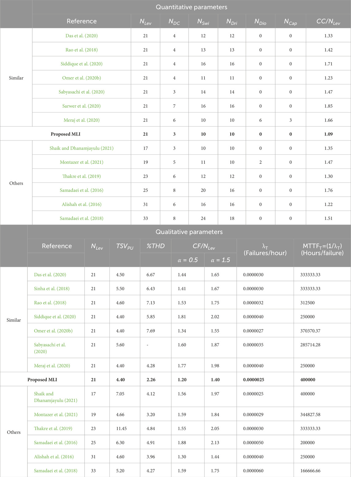
Therefore, CF/NLev for the suggested 21-level MLI topology with α values of 0.5 and 1.5 are 1.20 and 1.409, respectively.
4.3 Power loss and efficiency calculation
Two notable power losses occur in multilevel inverters: conduction (PCond) and switching losses (PSwil). Total conduction loss is determined by summing the conduction losses of both IGBTs (PCSW) and anti-parallel diodes (PCD) along the current path (Prasad and Dhanamjayulu, 2022). This can be expressed using Equations 31, 32:
where im (4A) is the peak output current. The threshold voltages for power switches and diodes are VSwi (4 V) and VDio (0.7 V). Similarly, RSwi (0.001Ω) and RDio (0.001Ω) represent the power switch on-state resistance and diode, respectively. The datasheet specifies β (0.01) as the power switch specification constant. If NSwi and NDio are the switches and diodes are conducting at the same time (t) to produce each level, then the average conduction loss is expressed using Equation 33:
Switching loss (PSwil) is the amount of power used when the switch turns on and off. This loss is calculated for the switch and the antiparallel diode. Equations 34–36 can be used to calculate the turn-on and -off energy loss (Eon, Eoff):
Similarly,
The time it takes to turn the switch off is toff, the time to turn it on is a ton, and the corresponding losses from the switch are Eoff-q and Eon-q, respectively. Although VSW q represents the voltage of the switch when it is in the off state, I and II represent the currents before and after the switch is turned on, respectively. The total switching losses can be calculated by Equation 37:
The fundamental frequency is denoted by f, Non-q, and Noff,-q, and the number of times that the qth switch is turned on or off during a single fundamental cycle. Therefore, the overall power losses is expressed using Equation 38:
The output power can thus be calculated by Equation 39:
The total efficiency (η) can be calculated using Equation 40:
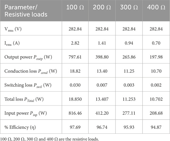
where Poutp and Pinp are the output and input powers. Table 6 summarizes the power losses and efficiency of the suggested MLI. The efficiency for various loads is graphically illustrated in Figure 16.
4.4 Reliability assessment
The reliability study determines the equipment’s predicted lifetime and failure rate, which are crucial to determining the health of any electronic device. Manufacturing organizations can profit from this reliability study as they seek long-lasting, high-performing, and low-maintenance products, and the industry can also estimate the mean time-to-repair and mean downtime to resume operations (Figure 17A). Therefore, an estimation of how long a device will survive is essential. To determine a device’s reliability, several factors are considered.
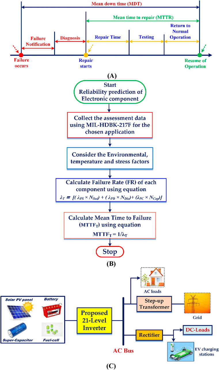
Figure 17. (A) Mean downtime and mean time to repair a generic component. (B) Flowchart of reliability analysis. (C) Applications of the proposed MLI.
MTTFT and FRT are the key reliability assessment requirements. The hazard rate (λT) is a prediction of failure over a certain timeframe. When FR is time-invariant, R(t) is reliability. Approximation and precise methods are preferred in power electronic circuit reliability testing. The mean time to the first failure is initially calculated to determine device durability. A high mean-time-to-failure (MTTFT) indicates reliability. This and the failure rate (FRT) of a device can be determined using MIL-HDBK 217E standard handbooks (Shaik et al., 2023). The approximation approach simplifies and accurately predicts FRT values for switches, diodes, and capacitors (mentioned in detail in Table 7), and the flowchart is shown in Figure 17B to calculate the MTTFT value.

Table 7. Failure rates of each component using the approximation method (Shaik et al., 2023).
Furthermore, as shown in Figure 17C, the suggested MLI keeps its self-voltage balanced, a unique quality that makes it suitable for a wide range of applications such as solar PV systems, fuel cells, battery-powered applications, and industrial generators. In addition, the suggested MLI might be used in medium-power micro-grids and grid configurations, offering a reliable solution for the problem of remote electrification.
The total MTTFT is estimated from power electronic circuit element FR values. Equation 41 is used to calculate λT:
Equation 42 is used to calculate the power electronic circuit MTTFT:
The suggested MLI architecture was compared with numerous quantitative features of the existing MLI topologies, including the number of DC sources (NDC), power switches (NSwi), gate drivers (NDri), diodes (NDio), capacitors (NCap), and component count per number of levels (CC/NLev). When it comes to qualitative comparisons such as the TSVpu, THD, CF, FRT, and MTTFT features, Table 8 presents quantitative and qualitative comparisons of the proposed 21-level MLI with existing topologies. All these comparisons indicate that the suggested 21-level MLI architecture is more economical, cost-effective, and achieves better performance outcomes.
5 Conclusion and future scope
This research proposed a novel 21-level MLI architecture for solar PV energy systems with fewer components. In addition, an EINC-based MPPT technique was used for constant PV panel power generation, even in partially shaded situations. The proposed MLI was tested for different loads, including R, RL, R-RL, and RL-R loads. The suggested MLI is simulated in MATLAB/Simulink and validated experimentally using hardware. The qualitative and quantitative comparative analysis with existing architectures demonstrates that the price, size, and TSV of the proposed MLI are reduced. The efficiency is 97.69%, and the CF/NLev for different weight coefficient (α = 0.5 and α = 1.5) values is 1.20 and 1.40, respectively. The reliability study parameter of λT is 0.0000025 failures/hour and MTTFT of 400000 h/failure are improved from the findings. The simulated THD is 2.06%, and the experimental THD is 2.26% under the IEEE standards. This suggested architecture can provide high-quality power from PV systems and improve power quality, voltage, and reactive power support for grid-connected systems, FACTS, RES, and EV applications. This research can also be appropriate for a battery storage system that the hotel and residential sectors can supply for emergency and standalone services.
Data availability statement
The raw data supporting the conclusions of this article will be made available by the authors, without undue reservation.
Author contributions
SN: conceptualization, formal analysis, investigation, methodology, software, validation, visualization, writing–original draft, and writing–review and editing. CD: investigation, methodology, project administration, resources, supervision, validation, visualization, and writing–review and editing.
Funding
The authors declare that no financial support was received for the research, authorship, and/or publication of this article.
Conflict of interest
The authors declare that the research was conducted in the absence of any commercial or financial relationships that could be construed as a potential conflict of interest.
Publisher’s note
All claims expressed in this article are solely those of the authors and do not necessarily represent those of their affiliated organizations, or those of the publisher, the editors, and the reviewers. Any product that may be evaluated in this article, or claim that may be made by its manufacturer, is not guaranteed or endorsed by the publisher.
References
Akbari, A., Ebrahimi, J., Jafarian, Y., and Bakhshai, A. (2022). A multilevel inverter topology with an improved reliability and a reduced number of components. IEEE J. Emerg. Sel. Top. Power Electron. 10 (1), 553–563. doi:10.1109/jestpe.2021.3089867
Alhassane Soumana, R., Juma Saulo, M., and Maina Muriithi, C. (2022). New control strategy for multifunctional grid-connected photovoltaic systems. Results Eng. 14, 100422. doi:10.1016/j.rineng.2022.100422
Ali Khan, M. Y., Liu, H., Yang, Z., and Yuan, X. (2020). A comprehensive review on grid connected photovoltaic inverters, their modulation techniques, and control strategies. Energies 13 (16), 4185. doi:10.3390/en13164185
Alishah, R. S., Hosseini, S. H., Babaei, E., and Sabahi, M. (2017). Optimal design of new cascaded switch-ladder multilevel inverter structure. IEEE Trans.Ind. Electron. 64 (3), 2072–2080. doi:10.1109/tie.2016.2627019
Alishah, R. S., Hosseini, S. H., Babaei, E., and Sabahi, M. (2016). A new general multilevel converter topology based on cascaded connection of sub multilevel units with reduced switching components, DC sources, and blocked voltage by switches. IEEE Trans. Ind. Electron. 63 (11), 7157–7164. doi:10.1109/tie.2016.2592460
Babaei, E., Laali, S., and Alilu, S. (2014). Cascaded multilevel inverter with series connection of novel H-bridge basic units. IEEE Trans. Ind. Electron. 61 (12), 6664–6671. doi:10.1109/tie.2014.2316264
Bana, P. R., Panda, K. P., Naayagi, R. T., Siano, P., and Panda, G. (2019). Recently developed reduced switch multilevel inverter for renewable energy integration and drives application: topologies, comprehensive analysis and comparative evaluation. IEEE Access 7, 54888–54909. doi:10.1109/access.2019.2913447
Chappa, A., Gupta, S., Sahu, L. K., Gautam, S. P., and Gupta, K. K. (2021). Symmetrical and asymmetrical reduced device multilevel inverter topology. IEEE J. Emerg. Sel. Top. Power Electron. 9 (1), 885–896. doi:10.1109/jestpe.2019.2955279
Das, D., Das, P., Pal, P. K., Mahto, K. k., and Mahato, B. (2024). Design, implementation and validation of a new multi-level topology with fewer components. Microsyst. Technol. 30, 1341–1352. doi:10.1007/s00542-023-05592-w
Das, M. K., Chauhan, S. S., Buduma, P., Jana, K. C., and Ishara, S. (2020). “A hybrid novel cascaded asymmetrical 21-level inverter with reduced switches,” in 2020 3rd International Conference on Energy, Power and Environment: Towards Clean Energy Technologies, Shillong, Meghalaya, India, 1–6. doi:10.1109/ICEPE50861.2021.9404463
Das, M. K., Jana, K. C., and Sinha, A. (2018). Performance evaluation of an asymmetrical reduced switched multilevel inverter for a grid-connected PV system. IET Renew. Power Gener. 12 (2), 252–263. doi:10.1049/iet-rpg.2016.0895
Hosseinzadeh, M. A., Sarebanzadeh, M., Rivera, M., Babaei, E., and Wheeler, P. (2021). A reduced single-phase switched-diode cascaded multilevel inverter. IEEE J. Emerg. Sel. Top. Power Electron. 9 (3), 3556–3569. doi:10.1109/jestpe.2020.3010793
Krishnachaitanya, D., and Chitra, A. (2021). Quantitative analysis of asymmetric multilevel inverters with reduced device count from reliability and cost function perspective—a review. IEEE Trans. Power Electron. 36 (10), 11068–11086. doi:10.1109/tpel.2021.3071375
Kumar, D., Nema, R. K., Gupta, S., Nema, S., and Dewangan, N. K. (2022). A new fault-tolerant multilevel inverter topology with enhanced reliability for PV application. Arabian J. Sci. Eng. 47 (11), 14841–14858. doi:10.1007/s13369-022-06992-2
Majeed Shaikh, A., Fawad Shaikh, M., Ahmed Shaikh, S., Krichen, M., Ali Rahimoon, R., and Qadir, A. (2023). Comparative analysis of different MPPT techniques using boost converter for photovoltaic systems under dynamic shading conditions. Sustain. Energy Technol. Assessments 57, 103259. doi:10.1016/j.seta.2023.103259
Meraj, S. T., Yahaya, N. Z., Hasan, K., and Masaoud, A. (2020). Single phase 21 level hybrid multilevel inverter with reduced power components employing low frequency modulation technique. Int. J. Power Electron. Drive Syst. 11 (2), 810. doi:10.11591/ijpeds.v11.i2.pp810-822
Montazer, B. H., Olamaei, J., Hosseinpour, M., and Mozafari, B. (2021). A generalized diode containing bidirectional topology for multilevel inverter with reduced switches and power loss. ’’ Int. J. Circuit Theory Appl. 49 (9), 2959–2978.
Mustafa, U., Arif, M. S. B., Kennel, R., and Abdelrahem, M. (2022). Asymmetrical eleven-level inverter topology with reduced power semiconductor switches, total standing voltage and cost factor. IET Power Electron. 15 (5), 395–411. doi:10.1049/pel2.12238
Narendra Babu, P. (2024). Adaptive grid-connected inverter control schemes for power quality enrichment in microgrid systems: past, present, and future perspectives. Electr. Power Syst. Res. 230, 110288. doi:10.1016/j.epsr.2024.110288
Nyamathulla, S., and Chittathuru, D. (2023). A review of multilevel inverter topologies for grid-connected sustainable solar photovoltaic systems. Sustainability 15, 13376. doi:10.3390/su151813376
Omer, P., Kumar, J., and Singh Surjan, B. (2020a). A review on reduced switch count multilevel inverter topologies. IEEE Access 8, 22281–22302. doi:10.1109/access.2020.2969551
Omer, P., Kumar, J., and Surjan, B. S. (2020b). A review on reduced switch count multilevel inverter topologies. IEEE Access 8, 22281–22302. doi:10.1109/access.2020.2969551
Prasad, D., and Dhanamjayulu, C. (2022). Reduced voltage stress asymmetrical multilevel inverter with optimal components. IEEE Access 10, 53546–53559. doi:10.1109/access.2022.3176110
Prasad, D., Dhanamjayulu, C., Padmanaban, S., Holm-Nielsen, J. B., Blaabjerg, F., and Khasim, S. R. (2021). Design and implementation of 31-level asymmetrical inverter with reduced components. IEEE Access 9, 22788–22803. doi:10.1109/access.2021.3055368
Rahimi, T., Fallah, M., Pashajavid, E., Pou, J., Arefi, A., and Loo, K. H. (2023). Single-phase 15-level inverters for uninterruptible power supply applications: fault-tolerant strategies. IEEE Trans. Consumer Electron. 69 (4), 1055–1067. doi:10.1109/tce.2023.3320632
Rao, S. N., Kumar, D. V. A., and Babu, C. S. (2018). Grid connected distributed generation system with high voltage gain cascaded DC-DC converter fed asymmetric multilevel inverter topology. Int. J. Electr. Comput. Eng. 8 (6), 4047. doi:10.11591/ijece.v8i6.pp4047-4059
Sabyasachi, S., Borghate, V. B., and Maddugari, S. K. (2020). A 21-level bipolar single-phase modular multilevel inverter. J. Circuits, Syst. Comput. 29 (1), 2050004. doi:10.1142/s0218126620500048
Samadaei, E., Gholamian, S. A., Sheikholeslami, A., and Adabi, J. (2016). An envelope type (E-type) module: asymmetric multilevel inverters with reduced components. IEEE Trans. Ind. Electron. 63 (11), 7148–7156. doi:10.1109/tie.2016.2520913
Samadaei, E., Sheikholeslami, A., Gholamian, S. A., and Adabi, J. (2018). A square T-type (ST-type) module for asymmetrical multilevel inverters. IEEE Trans. Power Electron. 33 (2), 987–996. doi:10.1109/tpel.2017.2675381
Sarwer, Z., Siddique, M. D., Iqbal, A., Sarwar, A., and Mekhilef, S. (2020). An improved asymmetrical multilevel inverter topology with reduced semiconductor device count. Int. Trans. Electr. Energy Syst. 30, e12587. doi:10.1002/2050-7038.12587
Shaik, N., Chittathuru, D., and Muyeen, S. M. (2023)1944). An overview of multilevel inverters lifetime assessment for grid-connected solar photovoltaic applications. Electronics 12 (8), 1944. doi:10.3390/electronics12081944
Shaik, N., and Dhanamjayulu, C. (2021). “Design of 17-level inverter with reduced switch count,” in 2021 innovations in power and advanced computing technologies (i-PACT) (IEEE), 1–8.
Siddique, M. D., Iqbal, A., Memon, M. A., and Mekhilef, S. (2020). A new configurable topology for multilevel inverter with reduced switching components. IEEE Access 8, 188726–188741. doi:10.1109/access.2020.3030951
Siddique, M. D., Mekhilef, S., Shah, N. M., and Memon, M. A. (2019). Optimal design of a new cascaded multilevel inverter topology with reduced switch count. IEEE Access 7, 24498–24510. doi:10.1109/access.2019.2890872
Sinha, A., Jana, K. C., and Das, M. K. (2018). An inclusive review on different multilevel inverter topologies, their modulation and control strategies for a grid connected photovoltaic system. Sol. Energy 170, 633–657. doi:10.1016/j.solener.2018.06.001
Tayyab, M., Sarwar, A., Murshid, S., Tariq, M., Al-Durra, A., and Bakhsh, F. I. (2023). Active and reactive power control of grid connected single-phase asymmetrical eleven-level inverter. IET Generation, Transm. and Distribution 17 (3), 632–644. doi:10.1049/gtd2.12442
Tayyab, M., Sarwar, A., Murshid, S., Tariq, M., Urooj, S., and Khan, B. (2022). Grid-connected operation and control of single phase asymmetrical multilevel inverter for distributed power generation. IET Renew. Power Gener. 16 (16), 3629–3642. doi:10.1049/rpg2.12581
Thakre, K., Mohanty, K. B., Chatterjee, A., and Kommukuri, V. S. (2019). A modified circuit for symmetric and asymmetric multilevel inverter with reduced components count. ’’ Int. Trans. Electr. Energy Syst. 29 (6), e12011. doi:10.1002/2050-7038.12011
Nomenclature
α weight coefficient value
Eon, Eoff energy consumption of on–off switches
STM standard testing measurement
Rse, Rpa series and shunt resistances of the PV cell equivalent circuit
K Boltzmann constant
T temperature
δ duty cycle of boost converter
fS switching frequency
THD total harmonic distortion
CF/NLev cost function per level
TSVpu total standing voltage per unit
VOC open-circuit voltage of the PV module
ISC short-circuit current of the PV module
IDi saturation current of a diode
MPPT maximum power point tracking
EINC enhanced incremental conductance
P&O perturb and observe
VSuni voltage stress on unidirectional switch
Vref reference voltage
λT total failure rate
λPS/λPD/λPC failure rate of switches/failure rate of diodes/failure rate of capacitors
MTTFT total mean time to failure
Vrms/Irms output RMS voltage and current
VSbi voltage stress on bidirectional switch
PTotal total power loss
G irradiance
Vcr carrier signal voltage
TR reference temperature
NSwi/NDri number switches/number of gate driver circuits
VSwi voltage across the ith switch
FRT failure rate
NCap/NDio number capacitors/number of diodes
RSwi/RDio resistance of the switch/resistance of diode
Vm maximum voltage of the reference signal
Ma modulation index
Vdc DC source voltage
NLev/NDC number of levels/number of DC sources
β power switch specification constant
Pswil switching power losses
Pcond conduction power losses
Poutp output power
Pinp input power
im maximum output current
PCSW/PCD conduction power loss of switches/conduction power loss of diodes
t total time period
toff/ton turn-off and turn-on timings
Keywords: cost function, level-shifted constant multicarrier sinusoidal pulse width modulation, multilevel inverter, PV boost SIMO converter, total harmonic distortion, total standing voltage
Citation: Nyamathulla S and C. D (2024) Design and implementation of a PV-tied effective inverter with high reliability and low THD for distribution-grid applications. Front. Energy Res. 12:1498514. doi: 10.3389/fenrg.2024.1498514
Received: 19 September 2024; Accepted: 30 October 2024;
Published: 04 December 2024.
Edited by:
Chee Wei Tan, University of Technology Malaysia, MalaysiaReviewed by:
Salman Ahmad, Islamic University of Science and Technology, IndiaBin Duan, Shandong University, China
Copyright © 2024 Nyamathulla and C. This is an open-access article distributed under the terms of the Creative Commons Attribution License (CC BY). The use, distribution or reproduction in other forums is permitted, provided the original author(s) and the copyright owner(s) are credited and that the original publication in this journal is cited, in accordance with accepted academic practice. No use, distribution or reproduction is permitted which does not comply with these terms.
*Correspondence: Dhanamjayulu C., ZGhhbmFtamF5dWx1LmNAdml0LmFjLmlu
 Shaik Nyamathulla
 Dhanamjayulu C.