 Qinhai Yu
 Chuang Liu
 Dongbo Guo
94% of researchers rate our articles as excellent or good
Learn more about the work of our research integrity team to safeguard the quality of each article we publish.
Find out more
ORIGINAL RESEARCH article
Front. Energy Res. , 02 May 2024
Sec. Sustainable Energy Systems
Volume 12 - 2024 | https://doi.org/10.3389/fenrg.2024.1375888
This article is part of the Research Topic Emerging Technologies for the Construction of Renewable Energy-Dominated Power System View all 32 articles
This paper proposes an input-parallel output-series (IPOS) Si-SiC hybrid inverter with dual-frequency harmonic elimination modulation strategy. The proposed topology composed of two power conversion cells and a three-phase five-column medium-frequency step-down transformer, the low-frequency power conversion cell (LFPC-C, 1 kHz) leverages strong current-carrying capacity of silicon-based devices for dealing with the system main power, and the high-frequency power conversion cell (HFPC-C, 30 kHz) based on wide-bandgap semiconductor SiC devices is used to addressing the fractional harmonics compensation power. This topology combines the strong current carrying capability of Si devices with the low switching loss of SiC devices at high frequency and achieves high quality power conversion at low cost and low loss. Compared to existing “IPOP” Si-SiC hybrid inverters, this topology adopts a coupling step-down transformer on the output side of both LFPC-C and HFPC-C, which can effectively reduce current stress of HFPC-C SiC devices. Additionally, a dual-frequency harmonic elimination modulation strategy based on the topology is proposed to solve the fractional harmonics caused by the LFPC-C. The paper establishes a mathematical model according to the harmonic distribution characteristics of the LFPC-C and HFPC-C, and designs the system control schedules. Building upon the derivation of the voltage ripple model and the design of hardware parameters, Si IGBT and SiC MOSFET were selected for constructing a 7.5 kW prototype for testing, and the experimental results validate the feasibility of this topology and the accuracy of theoretical analysis.
SiC MOSFET devices, leveraging their superior material properties, have become a key factor in enhancing the efficiency and power density of inverters, especially in high-frequency applications (Millán et al., 2014). The efficiency of inverters can reach as high as 99.4% (Miyazaki et al., 2018). Currently, SiC MOSFET devices have been successfully applied in naval and equipment power supply (Jones et al., 2016; Anurag et al., 2022), microgrids (Burkart and Kolar, 2017), and MMC (He et al., 2022).
However, SiC devices are costly and have a smaller current capacity, resulting in their rated power being lower than Si devices at the same voltage level. As shown in Figure 1, at high currents, the current cost of SiC devices is significantly higher than that of Si devices. Therefore, it is necessary to maximize the advantages of SiC devices in high-power scenarios while reducing the cost of the inverter. Currently, to overcome the limitation of the low rated current of SiC devices, scholars are combining Si devices with SiC devices. This combination leverages the low switching loss characteristics of SiC devices and the strong current-carrying capacity and cost-effectiveness of Si devices. The design approach of using both types of devices together brings about good electrical power quality and efficiency at a cost lower than a full SiC device design. There are two solutions to address this: one is to parallel SiC devices with Si devices at the switch device level to form a Si-SiC hybrid switch (Rahimo et al., 2015; Song et al., 2015; Zhao and He, 2015; Zhang et al., 2018); the other is based on the principle of Fractional Power Processing (Di Gioia and Brown, 2015; Kundu et al., 2020) at the topology level, constituting a Si-SiC hybrid inverter.
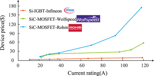
Figure 1. Price comparison between Si IGBT and SiC MOSFET from mainstream manufacturer.
The Si-SiC hybrid switch, as shown in Figure 2, can apply gate-source drive voltage to the SiC MOSFET and gate-emitter drive voltage to the Si-IGBT respectively. The turn-on delay and turn-off delay ensure zero voltage turn-on and turn-off of Si-IGBT, reducing switching losses and improving the efficiency and load capacity of the entire system (Li et al., 2020a). Reference (Deshpande and Luo, 2019) proposed an algorithm using dynamic junction temperature prediction to select the optimal Si-SiC current ratio, ensuring reliable operation of the hybrid switch. Reference (Li et al., 2020b) introduced an active gate delay control strategy based on an electro-thermal coupling loss model. This strategy dynamically adjusts and optimizes the gate delay time according to the operating conditions of the power converter, minimizing the working junction temperature difference between the two internal devices. Reference (Woldegiorgis et al., 2023) provided a comprehensive review and performance comparison of existing gate control strategies, gate driver designs, and packaging methods for Si-SiC hybrid switches. Design principles and guidelines were given for gate control strategies. However, significant progress in the commercial manufacture of Si-SiC hybrid switch modules has yet to be achieved.
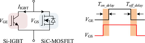
Figure 2. Si-SiC hybrid switch.
Currently, most Si-SiC hybrid converters based on the Fractional Power Processing (FPP) principle consist of two parallel parts, as shown in Figure 3: one part comprises Si IGBT devices operating at low frequency to handle the main power, while the other part consists of SiC MOSFET devices operating at high frequency to process only a small portion of the total power. Both parts are connected in parallel on the input and output sides, forming an input-parallel and output-parallel structure. The Si-SiC hybrid converter divides the power processing path into two parallel paths. By setting the switching information of the S IGBT and SiC MOSFET devices, the continuous energy signal is converted into two discrete energy signals with different numerical values. These signals are then reconstructed and combined into the final continuous energy output through passive components (Kundu et al., 2021; Wang et al., 2022). Compared to topologies with all SiC MOSFET devices, this kind of topology achieves a reduction in circuit cost while maintaining almost the same efficiency and power quality. Based on intelligence particle swarm optimization (PSO), reference (Zhang et al., 2023) propose a novel adaptive power-sharing and switching frequency control, it can reduce the power losses of the Si-SiC hybrid converter through a simple fitness function. Reference (Endres and Ackva, 2015) proposes a combination topology where the converter composed of Si-IGBT devices carries the main load current, while the converter composed of SiC MOSFET devices is used for ripple current compensation. A common-mode current suppression strategy for this combined topology is also proposed. Reference (Judge and Finney, 2019) verifies that the parallel hybrid converter significantly increases the effective switching frequency at the megawatt power level, reducing the need for external filters and increasing the current control bandwidth of the converter. References (Wu et al., 2022; Wu et al., 2019) design a ripple compensation direct digital control strategy that attenuates low-frequency current ripple to a small level and increases the frequency of the output current ripple, thereby reducing the volume and weight of the filter. Reference (Zhang et al., 2022) summarizes the characteristics of the input-parallel and output-series hybrid topology based on the FPP principle and proposes a hybrid bridge arm design method based on current harmonic elimination. The proposed design method can be implemented in various converters and has been validated in a bidirectional DC/DC converter. Unlike the “input-parallel and output-series “structure in the aforementioned references, the converter proposed in reference (Liu et al., 2022) has a parallel DC input and a series AC output through a transformer on the AC side, forming a “input-parallel and output-series” structure, aimed at harmonic control of the inverter output voltage.
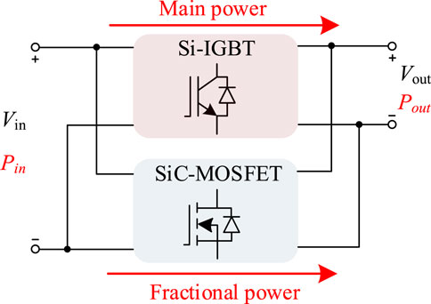
Figure 3. Si-SiC hybrid converter.
Based on the concept of Fractional Power Processing (FPP), this paper introduces a hybrid Si-SiC three-phase inverter composed of Si IGBT and SiC MOSFET devices, following the “input-parallel and output-series” topology structure. The low-frequency power conversion cell (LFPC-C) consists of Si IGBT devices and LC filters to handle the main power output. The high-frequency power conversion cell (HFPC-C) is composed of SiC MOSFET devices and LC filters, designed to compensate for the harmonics generated in the LFPC-C. The outputs of the LFPC-C and HFPC-C are connected in series through a three-phase five-column intermediate voltage transformer, reducing the current stress on SiC MOSFET in the HFPC-C. This topology leverages the strong conduction capabilities of Si IGBT and the low switching losses of SiC MOSFET during high-frequency operation. The proposed hybrid modulation strategy and coordinated control method, “LFPC-C open-loop, HFPC-C closed-loop” reduce the complexity of the control system. Hardware design methods are also presented based on the frequency characteristics of the LFPC-C and HFPC-C.
The rest of this article is organized as follows. Section 2 introduces the topology principle and dual-frequency harmonic elimination modulation strategy. In Section 3, it derives the frequency-domain mathematical model and proposes the control method. Section 4 analyzes its hardware characteristics, proposes a voltage ripple analysis model, and outlines the design principles for the filter and three-phase five-column medium-frequency step-down transformer. In Section 5, the feasibility of the topology is validated through the experimental setup. Finally, Section 6 concludes this article.
The proposed hybrid Si-SiC three phase inverter topology, as shown in Figure 4, consists of a low-frequency power conversion cell (LFPC-C),a high-frequency power conversion cell (HFPC-C) and a three-phase five-column medium-frequency step-down transformer. The input side is parallel and shared by a common DC source, and the outputs are coupled in series through the transformer. The LFPC-C employs Si IGBT devices as switching devices denoted as S1 ∼ S6, operating at a low switching frequency to deal with the main power of the proposed three-phase inverter. The HFPC-C uses SiC MOSFET devices as switching devices denoted as Q1 ∼ Q6, operating at a high switching frequency to handle fractional power. The transformer turns ratio is denoted as k, with the primary side parallel-coupled to the output filtering capacitor of the HFPC-C and the secondary side series-coupled and connected to the LFPC-C.
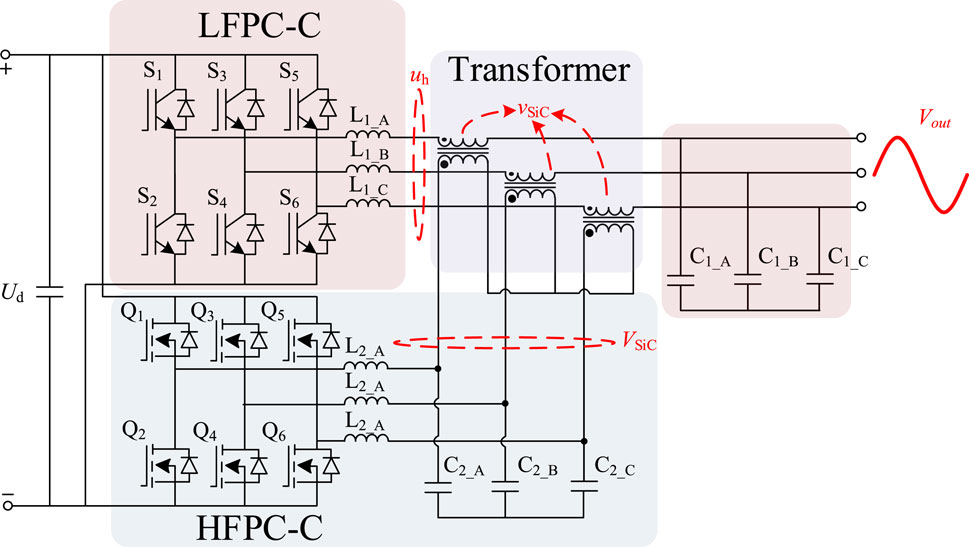
Figure 4. The proposed hybrid Si-SiC three phase inverter topology.
This topology realizes power sharing in two power conversion cells. Under the same DC side voltage, this topology reduces the switching losses of Si IGBT devices in the LFPC-C. Additionally, the step-down transformer ensures that the working current in the HFPC-C is less than the output current in the LFPC-C, reducing the current stress on SiC MOSFET devices and lowering on-state losses in the HFPC-C. The switching losses are concentrated on SiC MOSFET devices, and leveraging their excellent characteristics helps reduce the system’s overall switching losses.
The LFPC-C is responsible for the energy output of the system. However, due to its operation at a low frequency, it can lead to lower electrical energy quality in the final output of the system. Therefore, the HFPC-C needs to compensate and eliminate some of the harmonics present in the LFPC-C t to enhance the overall electrical energy quality of the system. The final output voltage of the system is composed of the voltage in the LFPC-C and the voltage on the secondary side of the transformer. The voltage in the LFPC-C is composed of the fundamental voltage and the harmonic voltage, while represents the output voltage of the HFPC-C. The relationship between these variables can be expressed as follows
The bridge arm output characteristics of the LFPC-C significantly impact the overall system performance. Specific Harmonic Elimination Pulse Width Modulation (SHEPWM) technology can eliminate particular harmonics, and the switching angles can be calculated through computations. SHEPWM operates at a low switching frequency, which helps in reducing the switching losses of the Si-IGBT devices. When using traditional SHEPWM to eliminate harmonics in the mid to low frequency range, it results in a large number of switching angles and necessitates a higher switching frequency. By serially connecting the HFPC-C and the transformer to the output circuit of the LFPC-C, certain harmonics in the bridge arm output of the LFPC-C can be eliminated. This approach ensures a reduction in the switching frequency of Si-IGBT devices in the LFPC-C, thus reducing switching losses while maintaining the total amount of eliminated output harmonics. In the HFPC-C, a Hybrid Sinusoidal Pulse Width Modulation (Hybrid SPWM) is employed. Hybrid SPWM refers to modulating the waveform, which is not a single-frequency sine wave but is determined by the superposition of multiple harmonic waves.
The collaborative elimination of mid to low-frequency harmonics by the LFPC-C and the HFPC-C involves segmenting the mid to low-frequency harmonics. Two technical approaches can be considered based on the harmonic distribution characteristics in the LFPC-C:
Method 1: The LFPC-C eliminates mid-frequency and high-frequency harmonics, while the HFPC-C eliminates low-frequency harmonics.
Method 2: The LFPC-C eliminates low-frequency and high-frequency harmonics, and the HFPC-C eliminates mid-frequency harmonics.
According to the residual harmonic distribution characteristics of SHEPWM (Cheng, 2021), both methods merely shift the harmonic energy to other frequency bands. However, when employing Method 2, where the LFPC-C eliminates low-frequency and high-frequency harmonics, and the mid-frequency harmonics are eliminated by the HFPC-C, it results in the HFPC-C handling harmonics excessively. The equivalent harmonic frequency within one power cycle can reach several kilohertz, demanding higher requirements for the control system and switching frequency of SiC MOSFET devices in the HFPC-C, thus increasing the switching losses of SiC MOSFET devices. Therefore, Method one is adopted, where the LFPC-C eliminates mid-frequency and high-frequency harmonics while the HFPC-C eliminates low-frequency harmonics. As illustrated in Figure 5A, the LFPC-C is responsible for system energy output, using SHEPWM to remove mid-frequency harmonics. The low-frequency harmonics are eliminated by the HFPC-C, and the high-frequency harmonics are eliminated by the LFPC-C’s filter. The HFPC-C compensates and eliminates low-frequency harmonics in the LFPC-C.
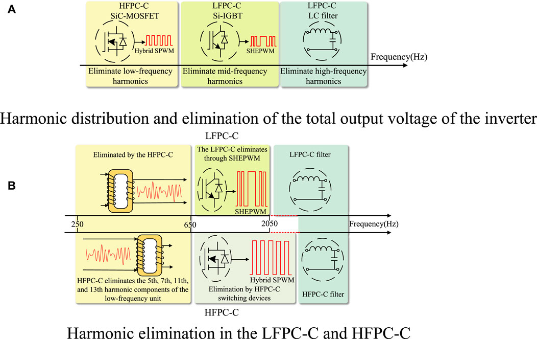
Figure 5. Harmonic distribution and elimination of the inverter.
When employing the first technical approach, the specific division of mid to low-frequency harmonics and the modulation degree of the hybrid modulated waves
The low-frequency harmonics to be eliminated in the LFPC-C represent a modulation signal composed of multiple harmonics for the HFPC-C. In SHEPWM modulation, once the fundamental modulation degree and switching angles are determined, the remaining harmonic superposition waveform becomes fixed. The LFPC-C uneliminated low-frequency harmonic family can be represented as
When a three-phase inverter is connected to a balanced load on the output side, The third harmonic and its multiples cancel each other out in the line-to-line voltage, hence we only need to focus on eliminating 6k±1 harmonics
In a three-phase half-bridge configuration, peak value of the output phase voltage
The variable
The transformer is a crucial coupling component connecting the LFPC-C and the HFPC-C. Through its turns ratio k, a relationship between Eqs 1, 2 is established, yielding the following correlation
The modulation index of the HFPC-C and the transformer turns ratio constrain each other. If the turns ratio k is chosen to be too large, it can lead to over-modulation in the HFPC-C. This over-modulation can introduce harmonics from other frequency bands into the output voltage of the LFPC-C, thereby degrading the quality of the output waveform. On the other hand, if the turns ratio k is chosen to be too small, it can cause the current in the HFPC-C to approach the output current in the main circuit, increasing the current cost of SiC MOSFET devices.
The LFPC-C in this paper is responsible for eliminating harmonics from the 17th to the 41st order. Meanwhile, the HFPC-C compensates and eliminates the fifth, seventh, 11th, and 13th order harmonics.
The bridge arm output voltage waveform of the LFPC-C using SHEPWM is shown in (Supplementary Figure S1).
The output waveform in Figure 6 is symmetric about a 1/4 period, and it can be represented using a Fourier series as follows
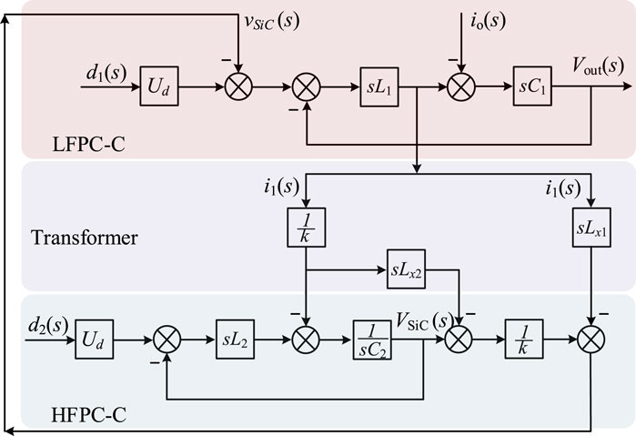
Figure 6. Mathematical model in frequency domain.
In the equation,
In the equation,
The HFPC-C employs hybrid sinusoidal pulse width modulation technique, where the modulation wave is composed of fifth, seventh, 11th, and 13th harmonic sinusoidal waves. The expression is:
Taking the modulation index m = 0.97 as an example, the schematic diagram of the modulated wave and the triangular carrier wave for the HFPC-C is shown in (Supplementary Figure S2).
In this section, based on the time-domain coupling relationship of the 2 cells mentioned above, a frequency-domain mathematical model is established. Frequency domain analysis of the system is conducted, and a control method for the system is proposed.
The mathematical model is as shown in Figure 6, and there are two switch degrees of freedom, denoted as
The relationship between
and
The relationship between
If the secondary-side leakage inductance is attributed to the LFPC-C filter inductance,
Let
Let
Let
Finally, we can obtain the following expression:
From Eqs 13, 14, it can be seen that the circuit has two degrees of freedom,
Since the control objective is to compensate for the secondary-side voltage of the transformer, fundamentally, the closed-loop control aims to control the secondary-side voltage of the transformer. Therefore, in designing the closed-loop control circuit, the effect of the LFPC-C current on the HFPC-C can be considered as a disturbance. We propose a coordinated control method, “LFPC-C open-loop, HFPC-C closed-loop”. In this approach, the LFPC-C uses open-loop SHEPWM control to adjust the voltage by only adjusting the fundamental modulation ratio, reducing the control difficulty for the HFPC-C. The HFPC-C achieves precise voltage regulation, compensating for the limitations of SHEPWM.
When processing the fifth, seventh, 11th, and 13th harmonic components in the HFPC-C and extracting the control system’s reference signal, the following two points need to be considered:
1) The physical sampling point is located between the inductance of the LFPC-C and the secondary side of the transformer. The sampled voltage still contains the uneliminated high-frequency harmonics, which are not the target of the HFPC-C tracking control.
2) Regarding the selected fifth, seventh, 11th, and 13th harmonic components frequency domain characteristics: zero gain and zero phase shift.
Considering the above two points, Recursive Discrete Fourier Transform is used to meet the aforementioned requirements. The expression is as follows:
Amplitude-frequency response and phase-frequency response of
The above equation yields the reference signal
Obtaining the current inner-loop reference signal
The response speed. Controlling the inner loop with the capacitor current as the control target can increase system damping, suppress resonance, and reduce the difficulty of voltage outer loop control.
The transfer function of the closed-loop control for the HFPC-C is
The overall control policy is shown in Supplementary Figure S4.
When considering voltage compensation by the HFPC-C for the LFPC-C, it is necessary to establish a steady-state voltage ripple model. The primary side of the series-coupled transformer is connected in parallel across the filtering capacitor of the HFPC-C. Neglecting the fundamental component in the circuit, the ripple in the primary-side voltage is equivalent to a voltage source
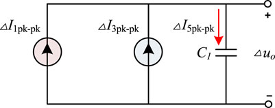
Figure 7. Equivalent circuit of LFPC-C ripple current source.
In the equation,
The total ripple current
The expression for the total output ripple voltage
The ripple analysis for the HFPC-C is illustrated in Figure 10.
The parameter
The ripple in the output current of the LFPC-C bridge arm is represented by
The total ripple current
The ripple voltage on the filter capacitor of the HFPC-C is represented by
Based on
Substituting into Eq. 26,
Supplementary Figure S7, Figure 8 in Additional files illustrates the ratio of output voltage ripple to DC voltage on the direct current (DC) side based on Eq. 31 for different parameters chosen for L1 and L2.
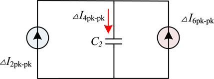
Figure 8. Equivalent circuit of ripple current source in HFPC-C.
As shown in Figure 5B above, the filters in the low-frequency and HFPC-C filter different ranges of harmonics. Additionally, the compensation of voltage ripples in the HFPC-C and the final circuit output ripples in the LFPC-C, as analyzed in the previous section, are closely related to the selection of passive components L1、L2、C1and C2 in the circuit. Considering the constraints mentioned above, frequency domain constraints also need to be taken into account.
For the LFPC-C, as shown in Figure 5B above, the harmonics from the 5th to the 13th order are eliminated through the HFPC-C, and the harmonics from the 17th to the 41st order are already eliminated through SHEPWM. The remaining harmonics in the high-frequency range are eliminated through a second-order low-pass LC filter. The cutoff frequency
Simultaneously, to prevent resonance peaks in the LFPC-C filter and to amplify the fifth, seventh, 11th, and 13th harmonics, increasing the compensation difficulty for the HFPC-C, requirements are imposed on the damping coefficient of the filter
The HFPC-C compensates for the highest harmonic frequency at 650 Hz. The selected switching frequency is 30 kHz, and the upper limit for the filter cutoff frequency
Due to the non-sinusoidal periodic components of the input terminal voltage injected into the transformer, which is a superposition of fifth, seventh, 11th, and 13th harmonic voltages, a three-phase five-column medium-frequency transformer is used. This ensures that the high-order harmonic flux can circulate smoothly, and harmonics can flow in the independent magnetic circuits of the three-phase five-column medium-frequency transformer (Leung et al., 2010). When the circuit operates normally, the highest harmonic frequency allowed to pass through is 650 Hz. This necessitates the transformer to have a relatively high passband. Additionally, due to the higher frequency of voltage polarity conversions, losses will increase. Therefore, thin silicon steel sheets are used for the transformer core. Thin silicon steel offers advantages such as high saturation magnetic flux density, ideal loss performance, and low noise. Transformer model is displayed in (Supplementary Figure S9). The length of the transformer is 45cm, the height is 25 cm and the width is 19 cm.
To ensure minimal voltage distortion, it is crucial to maintain the magnetic flux of the transformer in a non-saturated state and operate within the linear region (Li et al., 2011). The magnetic flux density
Based on the proposed inverter and control method in this paper, a laboratory prototype with a power rating of 7.5 kW was set up in this section. The experimental setup, as shown in Figure 9, includes a dSPACE controller, a LFPC-C, a HFPC-C, a load, a transformer, and a sampling circuit. The parameters and values used in the experiment are listed in Additional files (Supplementary Table 1).
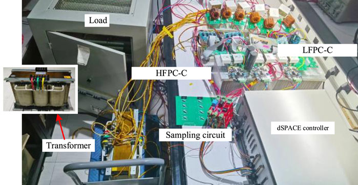
Figure 9. Experimental prototype.
The output voltage of the LFPC-C bridge arm is shown in Figure 10. It can be observed from Additional files (Supplementary Figure S10) that the bridge arm output voltage
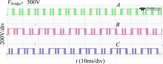
Figure 10. LFPC-C bridge arm output voltage.
During steady-state operation, the waveforms of the final output voltage
Figure 11 presents the Fourier Transform (FFT) analysis of
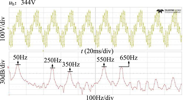
Figure 11. The voltage
Additional files (Supplementary Figure S13) shows the three phase voltage at the primary side of the transformer. Through FFT decomposition, it can be observed that the voltage contains harmonics at 250 Hz, 350 Hz, 550 Hz, and 650 Hz.
Figure 12 verifies the dynamic performance of the system. From the figure, it can be observed that the transient duration for the compensation of the LFPC-C by the HFPC-C is 23 m, demonstrating the rationality of the harmonic extraction and control design.
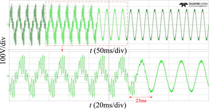
Figure 12. Dynamic response of HFPC-C compensation.
Supplementary Figure S14 displays the Fourier Transform (FFT) analysis of the output voltage
Supplementary Figure S15 shows the waveforms of total output voltage, output current, and transformer primary and secondary side voltages for phase A.
Figure 13 depicts the voltage waveform at a low modulation index of m = 0.4, with a peak value of 100V.
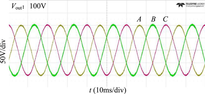
Figure 13. When m = 0.4, the final output voltage
Figure 14 and (Supplementary Figure S15) represent the FFT of
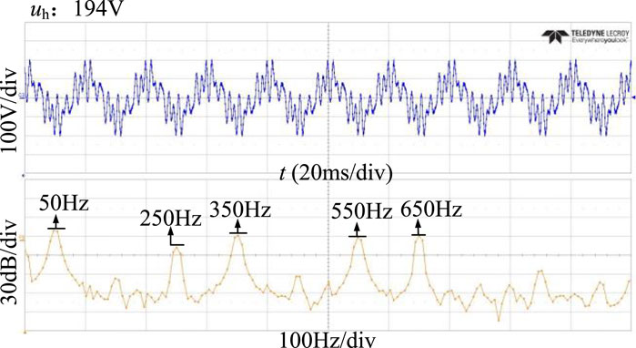
Figure 14. The voltage
To demonstrate the efficiency of the proposed converter, a theoretical comparison was made between the proposed converter, a hybrid switch converter, and an Si-IGBT converter. Considering high-power applications, the theoretical converter’s DC voltage was set to 800 V, and the efficiency curves are shown in Additional files (Supplementary Figure S17).
From (Supplementary Figure S17), it can be observed that the highest efficiency of the converter proposed in this paper is 98.3%. As the load percentage exceeds 50%, the efficiency of the proposed converter is even higher, demonstrating its advantages under high-power conditions.
From (Supplementary Figure S18), it is evident that under full load conditions, the switching losses of the low-frequency unit Si-IGBT account for only 4% of the total losses. Device losses are primarily concentrated in conduction losses. On the other hand, the device losses of the high-frequency unit SiC-MOSFET account for only 22% of the total losses.
In this article, based on fractional power processing, a “input-parallel and output-series” hybrid three-phase inverter consisting of Si IGBT and SiC MOSFET devices is proposed. The LFPC-C is formed by Si IGBT devices, and it employs SHEPWM modulation along with the HFPC-C to eliminate low-frequency and mid-frequency harmonics. This approach allows Si IGBT to handle the main power with minimal switching losses. The HFPC-C consists of SiC MOSFET devices, enabling it to accurately compensate for the LFPC-C low-frequency harmonics while operating with low switching losses. Three-phase five-column medium-frequency step-down transformer reduces the current flowing through the HFPC-C to approximately half of the inverter’s output current, minimizing the current stress on SiC MOSFET devices. This topology leverages the strong conduction capability of Si IGBT and the low switching losses of SiC MOSFET in high-frequency states to reduce device losses in high power conversion applications. Additionally, the proposed “LFPC-C open-loop, HFPC-C closed-loop” coordinated control method simplifies the control system. The ripple voltage analysis model, based on circuit characteristics, guides the passive component design. Task allocation for filtering and transformer components is determined according to the circuit’s requirements for harmonics elimination and compensation. Furthermore, a 7.5 kW experimental prototype is constructed to validate the feasibility of this proposed topology.
The original contributions presented in the study are included in the article/Supplementary Material, further inquiries can be directed to the corresponding author.
QY: Writing–original draft, Writing–review and editing. CL: Writing–original draft, Writing–review and editing, Conceptualization, Data curation, Formal Analysis, Funding acquisition, Investigation, Methodology, Project administration, Resources, Software, Supervision, Validation, Visualization. RL: Writing–original draft, Writing–review and editing, Conceptualization, Data curation, Formal Analysis, Funding acquisition, Investigation, Methodology, Project administration, Resources, Software, Supervision, Validation, Visualization. ZP: Writing–original draft, Writing–review and editing, Conceptualization, Data curation, Formal Analysis, Funding acquisition, Investigation, Methodology, Project administration, Resources, Software, Supervision, Validation, Visualization. DG: Writing–original draft, Writing–review and editing, Conceptualization, Data curation, Formal Analysis, Funding acquisition, Investigation, Methodology, Project administration, Resources, Software, Supervision, Validation, Visualization. TM: Conceptualization, Data curation, Formal Analysis, Funding acquisition, Investigation, Methodology, Project administration, Resources, Software, Supervision, Validation, Visualization, Writing–original draft, Writing–review and editing. XS: Writing–original draft, Writing–review and editing, Conceptualization, Data curation, Formal Analysis, Funding acquisition, Investigation, Methodology, Project administration, Resources, Software, Supervision, Validation, Visualization.
The author(s) declare that no financial support was received for the research, authorship, and/or publication of this article.
The authors declare that the research was conducted in the absence of any commercial or financial relationships that could be construed as a potential conflict of interest.
All claims expressed in this article are solely those of the authors and do not necessarily represent those of their affiliated organizations, or those of the publisher, the editors and the reviewers. Any product that may be evaluated in this article, or claim that may be made by its manufacturer, is not guaranteed or endorsed by the publisher.
The Supplementary Material for this article can be found online at: https://www.frontiersin.org/articles/10.3389/fenrg.2024.1375888/full#supplementary-material
Anurag, A., Acharya, S., Bhattacharya, S., Weatherford, T. R., and Parker, A. A. (2022). A gen-3 10-kV SiC MOSFET-based medium-voltage three-phase dual active bridge converter enabling a mobile utility support equipment solid state transformer. IEEE J. Emerg. Sel. Top. Power Electron. 10 (2), 1519–1536. doi:10.1109/jestpe.2021.3069810
Burkart, R. M., and Kolar, J. W. (2017). Comparative $\eta$– $\rho$– $\sigma$ pareto optimization of Si and SiC multilevel dual-active-bridge topologies with wide input voltage range. IEEE Trans. Power Electron. 32 (7), 5258–5270. doi:10.1109/tpel.2016.2614139
Cheng, J. (2021). Improved SHEPWM technology and its application in high-power grid-connected inverter. Hangzhou, China: Zhejiang Univ. Ph.D. dissertation, Dept. Electron. Eng.
Deshpande, A., and Luo, F. (2019). Practical design considerations for a Si IGBT + SiC MOSFET hybrid switch: parasitic interconnect influences, cost, and current ratio optimization. IEEE Trans. Power Electron. 34 (1), 724–737. doi:10.1109/tpel.2018.2827989
Di Gioia, A., and Brown, I. P. (2015). “Silicon and hybrid Si-SiC tandem inverter analytical loss characterization and comparison to PWM-modulated voltage source inverter,” in Proc. IEEE Energy Convers. Congr. Expo, Montreal, QC, Canada, 4664–4670. doi:10.1109/ecce.2015.7310319
Dong, Z., Wang, C., Zhou, M., Liu, M., and Li, K. (2024). Active NP voltage balance control strategy for three-level three phase inverter under SHEPWM. Transactions of China Electrotechnical Society 39 (04), 1147–1158. doi:10.19595/j.cnki.1000-6753.tces.222093
Endres, J., and Ackva, A. (2015). “A parallel three-phase converter system for ripple current compensation and passive filter reduction,” in Proc. 17th Eur. Conf. Power Electron, 1–9. Appl. doi:10.1109/epe.2015.7309135
He, Z., Lu, M., Hang, L., Zeng, P., and Liu, Y. (2022). Capacitor voltage imbalance mechanism and balancing control of MMC when riding through PTG fault. CSEE J. Power Energy Syst. to be published. doi:10.17775/CSEEJPES.2022.03810
Jones, E. A., Wang, F. F., and Costinett, D. (2016). Review of commercial GaN power devices and GaN-based converter design challenges. IEEE J. Emerg. Sel. Top. Power Electron. 4 (3), 707–719. doi:10.1109/jestpe.2016.2582685
Judge, P. D., and Finney, S. (2019). “2-level Si IGBT converter with parallel part-rated SiC converter providing partial power transfer and active filtering,” in Proc. 20th Workshop Control Model. Power Electron, 1–7. doi:10.1109/compel.2019.8769710
Kundu, A., Na, R., Amir, A., and Shen, Z. J. (2021). “Optimization strategy of WBG fractional power processing,” in Proc. IEEE Appl. Power Electron. Conf. Expo, 896–901. doi:10.1109/apec42165.2021.9487447
Kundu, A., Na, R., Amir, A., Zhou, Y., Brown, I. P., and Shen, Z. J. (2020). “WBG fractional power processing: a new Si-SiC hybrid voltage source inverter design,” in Proc. IEEE Energy Convers. Congr. Expo, 6226–6231. doi:10.1109/ecce44975.2020.9236129
Leung, C., Dutta, S., Baek, S., and Bhattacharya, S. (2010). “Design considerations of high voltage and high frequency three phase transformer for Solid State Transformer application,” in Proc. IEEE Energy Convers. Congr. Expo, 1551–1558. doi:10.1109/ecce.2010.5618234
Li, P., Dong, J., and Li, T. (2011). Design of coupling transformer in shunt active power filter. Electrotech. Appl. 30 (22), 25–27+35.
Li, Z., Wang, J., Deng, L., He, Z., Yang, X., Ji, B., et al. (2020b). Active gate delay time control of Si/SiC hybrid switch for junction temperature balance over a wide power range. IEEE Trans. Power Electron. 35 (5), 5354–5365. doi:10.1109/tpel.2019.2942044
Li, Z., Wang, J., He, Z., Yu, J., Dai, Y., and Shen, Z. J. (2020a). Performance comparison of two hybrid Si/SiC device concepts. IEEE J. Emerg. Sel. Top. Power Electron. 8 (1), 42–53. doi:10.1109/jestpe.2019.2947252
Liu, C., Zhuang, K., Pei, Z., Zhu, D., Li, X., Yu, Q., et al. (2022). Hybrid SiC-Si DC–AC topology: SHEPWM Si-IGBT master unit handling high power integrated with partial-power SiC-MOSFET slave unit improving performance. IEEE Trans. Power Electron. 37 (3), 3085–3098. doi:10.1109/tpel.2021.3114322
Mao, X., Ayyanar, R., and Krishnamurthy, H. K. (2009). Optimal variable switching frequency scheme for reducing switching loss in single-phase inverters based on time-domain ripple analysis. IEEE Trans. Power Electron. 24 (4), 991–1001. doi:10.1109/tpel.2008.2009635
Millán, J., Godignon, P., Perpiñà, X., Perez-Tomas, A., and Rebollo, J. (2014). A survey of wide bandgap power semiconductor devices. IEEE Trans. Power Electron. 29 (5), 2155–2163. doi:10.1109/tpel.2013.2268900
Miyazaki, T., Otake, H., Nakakohara, Y., Tsuruya, M., and Nakahara, K. (2018). A fanless operating trans-linked interleaved 5 kW inverter using SiC MOSFETs to achieve 99% power conversion efficiency. IEEE Trans. Ind. Electron 65 (12), 9429–9437. doi:10.1109/tie.2018.2816004
Rahimo, M., Canales, F., Minamisawa, R. A., Papadopoulos, C., Vemulapati, U., Mihaila, A., et al. (2015). Characterization of a silicon IGBT and silicon carbide MOSFET cross-switch hybrid. IEEE Trans. Power Electron. 30 (9), 4638–4642. doi:10.1109/tpel.2015.2402595
Song, X., Huang, A. Q., Lee, M., and Peng, C. (2015). “High voltage Si-SiC hybrid switch: an ideal next step for SiC,” in Proc. IEEE 27th Int. Symp. Power Semicond. Devices IC’s, 2015 IEEE 27th International Symposium on Power Semiconductor Devices IC's, 289–292. doi:10.1109/ispsd.2015.7123446
Wang, L., Sun, W., Xu, H., Dong, J., Li, C., and Li, W. (2022). “A three-phase-module-parallel Si and SiC hybrid inverter with smaller filter size and low cost,” in Proc. IEEE Transp. Electrific. Conf. Expo., Asia-Pacific, 1–6. doi:10.1109/itecasia-pacific56316.2022.9942026
Wang, Z., and Liu, J. (2009). “PWM control technology,” in Power electronics. 7th ed. (Beijing, China: China Machine Press), 167–168.
Woldegiorgis, D., Hossain, M. M., Saadatizadeh, Z., Wei, Y., and Mantooth, H. A. (2023). Hybrid Si/SiC switches: a review of control objectives, gate driving approaches and packaging solutions. IEEE J. Emerg. Sel. Top. Power Electron. 11 (2), 1737–1753. doi:10.1109/jestpe.2022.3219377
Wu, T.-F., Huang, Y.-H., Cheng, W.-C., and Gao, X.-C. (2019). “Ripple-compensation improvement of direct digital controlled 3Φ4W grid-connected hybrid-frequency inverter system,” in Proc. IEEE Appl. Power Electron. Conf. Expo, 284–289. doi:10.1109/apec.2019.8722232
Wu, T.-F., Huang, Y.-H., Temir, S., and Chan, C.-C. (2022). 3Φ4W hybrid frequency parallel uninterruptable power supply for reducing voltage distortion and improving dynamic response. IEEE Trans. Ind. Electron 10 (1), 906–918. doi:10.1109/jestpe.2021.3099061
Zhang, C., Wang, J., Qu, K., Hu, B., Li, Z., Yin, X., et al. (2022). WBG and Si hybrid half-bridge power processing toward optimal efficiency, power quality, and cost tradeoff. IEEE Trans. Power Electron. 37 (6), 6844–6856. doi:10.1109/tpel.2021.3138464
Zhang, C., Yuan, X., Wang, J., Chen, W., Hu, B., and Shen, Z. J. (2023). Adaptive power sharing and switching frequency control for power loss optimization in WBG/Si hybrid half-bridge converters. IEEE Trans. Power Electron 38 (4), 4440–4450. doi:10.1109/tpel.2022.3230747
Zhang, Z., Zhang, L., and Qin, J. (2018). “Optimization of delay time between gate signals for Si/SiC hybrid switch,” in Proc. IEEE Energy Convers. Congr. Expo, 1882–1886. doi:10.1109/ecce.2018.8557569
Keywords: fractional power processing, harmonic compensation, dual-frequency harmonic elimination modulation strategy, multiple quasi-proportional resonance control, recursive discrete fourier transform, SHEPWM, Si-SiC inverter
Citation: Yu Q, Liu C, Li R, Pei Z, Guo D, Mao T and Shao X (2024) Input-parallel output-series Si-SiC hybrid inverter with fractional harmonic elimination. Front. Energy Res. 12:1375888. doi: 10.3389/fenrg.2024.1375888
Received: 24 January 2024; Accepted: 04 April 2024;
Published: 02 May 2024.
Edited by:
Liansong Xiong, Xi’an Jiaotong University, ChinaReviewed by:
Donghai Zhu, Huazhong University of Science and Technology, ChinaCopyright © 2024 Yu, Liu, Li, Pei, Guo, Mao and Shao. This is an open-access article distributed under the terms of the Creative Commons Attribution License (CC BY). The use, distribution or reproduction in other forums is permitted, provided the original author(s) and the copyright owner(s) are credited and that the original publication in this journal is cited, in accordance with accepted academic practice. No use, distribution or reproduction is permitted which does not comply with these terms.
*Correspondence: Dongbo Guo, Z3VvZG9uZ2JvQG5lZXB1LmVkdS5jbg==
Disclaimer: All claims expressed in this article are solely those of the authors and do not necessarily represent those of their affiliated organizations, or those of the publisher, the editors and the reviewers. Any product that may be evaluated in this article or claim that may be made by its manufacturer is not guaranteed or endorsed by the publisher.
Research integrity at Frontiers
Learn more about the work of our research integrity team to safeguard the quality of each article we publish.