 Weilu Li
 Yongcan Huang
 Chunhua Liu2
 Agnes Valencia
 Walid A. Daoud
94% of researchers rate our articles as excellent or good
Learn more about the work of our research integrity team to safeguard the quality of each article we publish.
Find out more
ORIGINAL RESEARCH article
Front. Electron., 14 February 2025
Sec. Wearable Electronics
Volume 6 - 2025 | https://doi.org/10.3389/felec.2025.1501178
Introduction: Amidst the rapidly growing development of wearable electronics, their dependence on external power sources increases the power expense while leading to interruptions of their operation during charging. Biomechanical energy harvesters offer a promising solution for self-powered wearable electronics by converting waste kinetic energy to electricity. Despite successful efforts in advancing their power outputs from μW to mW, several challenges persist, including low output current at the μA-level, high internal impedance in the GΩ-level, and AC outputs, restricting their practical applications. Conventional power management circuits are commonly utilized in high-frequency harvesters without adequate consideration of the energy loss that incurs, potentially leading to circuit failure when used in low-frequency harvesters with a lower power output.
Methods: Here, we introduce a low-loss power management circuit (L-PMC) that functions under low-frequency conditions to facilitate biomechanical energy harvesting.
Results: Our innovative two-stage energy transfer strategy boosts the energy extraction efficiency to 42.24%, breaking previous records. With an energy transfer efficiency of 30.59%, L-PMC can charge a battery from 1.9 V to 2.4 V in just 10 min.
Discussion: Moreover, the integration of passive current amplification tripled charge accumulation and energy storage, representing 207% enhancement in energy transfer efficiency, presenting a versatile and universal approach to low-frequency biomechanical energy harvesting for new generation wearable electronics.
The power management circuit (PMC) plays a vital role in realizing the integration of renewable energy sources with energy storage systems, enabling efficient energy transfer to address the rising energy demand for new generation wearable electronics (Faisal et al., 2018; Xu et al., 2014; Abhinav and Pindoriya, 2016; Kaper and Choudhary, 2016; Nouri et al., 2024; Abdelsattar et al., 2024). Biomechanical energy harvesters (BEH), first reported in 2012 (Fan et al., 2012), convert ambient mechanical energy into electricity using electrification and electrostatic induction effects, offering a promising weather-independent and compact energy alternative compared to other renewable energy sources (Jiang et al., 2015; Wang, 2019; Zi and Wang, 2017; Zhang H. et al., 2024). However, as the device responds to external stimuli, the varying frequency and magnitude of mechanical energy inputs result in fluctuations in electricity generation, causing difficulties in energy integration and storage. Moreover, the typically high output voltage (up to kV-level), weak output current (μA-level), and AC outputs of BEH restricts their use as direct power sources or for battery charging, where a relatively low-voltage (V-level), high-current (mA to A-level), and DC electricity source is required. The mismatch between BEH sources and terminal appliances reduces the energy extraction and transfer efficiency, resulting in considerable energy loss. To address this problem, the integration of PMC is essential.
To date, PMCs have been studied for AC/DC conversion and capacitor charging when operating with a relatively greater current output from high-frequency BEH sources (Niu and Wang, 2015; Shankaregowda et al., 2016; Lee et al., 2014; Zhang Z. et al., 2024; Zhou et al., 2023; Wang et al., 2023). However, commercial full-wave bridge rectifier and capacitors often experience leakage currents, which can result in circuit failure when the current output from low-frequency BEH sources is much lower. This simple topology works well to temporarily store energy in capacitors for powering portable electronics, such as smartwatches and humidity meters (for seconds). However, its energy extraction and transfer efficiencies are very limited due to the mismatch between the internal impedance of BEH sources and external circuit load. Resistor-inductor-capacitor (RLC) impedance matching circuits with buck conversion functionality have been researched to improve energy extraction (Zhang Z. et al., 2024; Fang et al., 2020; Zhao et al., 2017; Kong et al., 2010; Wang et al., 2015). Inductors function in discontinuous mode, when their current direction changes within a single switch on-and-off cycle (Supplementary Figure S1), leading to an RLC series resonance phenomenon under light-loading (≤30%) or no-loading. Its pulse current and voltage electromagnetically interact with the BEH source, resulting in greater ripple, which requires additional filtration, resulting in energy loss and reduced energy transfer efficiency. In summary, BEH for battery charging has been minimally studied. Less efficient RLC impedance matching and high energy loss due to inappropriate component sizing reduce energy extraction and transfer efficiencies, respectively (Kong et al., 2010; Shi et al., 2022).
A low-loss PMC (L-PMC) technique is explored in this study for the purpose of weak biomechanical energy harvesting at low-frequency. Since the current and intermittence of BEH affect circuit efficiency and are determined by the operating frequency, we studied the PMC under extreme conditions at 1 Hz. The objective is to realize battery charging by reducing current ripple and energy loss, while attaining efficient energy extraction and transfer efficiency to fulfil the requirements of a reliable and readily available DC power source. This work incorporates two PMC topologies, as seen on Figure 1. Topology_1 is a 2-stage RC impedance matching circuit with buck conversion functionality. The analyzed Topology_1 achieves an energy extraction efficiency of 42.24% and can charge a battery to 20% in 10 min at a low operating frequency of 1 Hz. Topology_2 is a multi-capacitor unit for current amplification, further enhancing the energy transfer efficiency from 30.59% to 63.55%, representing 207% enhancement. The study is conducted in three phases: 1) mathematical derivation for impedance matching, 2) circuit topology design and simulation, and 3) experimental validation.
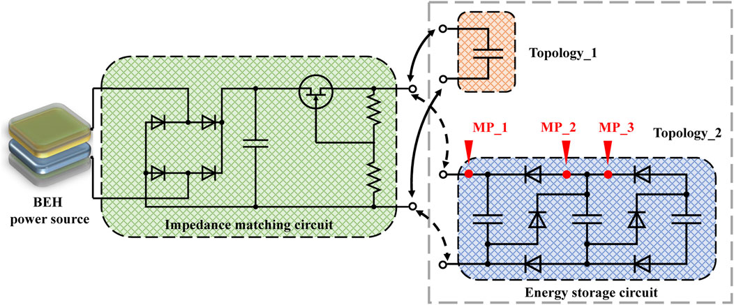
Figure 1. Schematic diagram of the proposed PMC topologies. Topology_1 and Topology_2 share a common impedance matching circuit. Topology_1 consists of a capacitor for energy storage. Topology_2 consists of multiple capacitors that are charged in series and discharged in parallel under the direction of diodes, realizing passive amplification. Three measuring points, namely, MP_1, MP_2, and MP_3, are analyzed during experimental validation.
A 3 cm × 3 cm contact-separation BEH device was fabricated as the power input of the PMC, with working principle as shown in Figure 2A (Wang et al., 2020). The device features Au/PEI/PVA as the tribo-positive layer, PET as the tribo-negative layer, and PET-ITO as the top and bottom electrodes. The device was packaged using Kapton tape, with a 2 mm air gap between the triboelectric layers. Upon pressing and releasing the device, the PET and Au/PEI/PVA layers became negatively and positively charged, respectively, due to their differing electronegativity. Externally, electrons flowed between the top to bottom electrodes, and the cyclic operating mode of the device resulted in an AC power output.
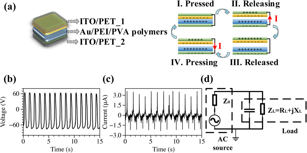
Figure 2. Schematic illustration of (A) contact-separation BEH and its working principle (I. to IV.). The BEH consists of ITO/PET as top and bottom inductive electrodes, and Au/PEI/PVA polymers as the triboelectric layers. During the pressing and releasing processes, the electrodes are induced positive and negative charges, resulting to a flow of electrons, and generating an AC signal as the electrodes are connected by external wires; (B) BEH’s open-circuit voltage output of 60 V; (C) BEH’s short-circuit current output of 3.3 μA; (D) equivalent circuit of the BEH. BEH is regarded as an AC source with an internal impedance of
The output performance of the BEH was measured using source meters (Keithley 2400 and 6514) and a low-noise current preamplifier (SR570). A linear motor (LinMot) supplied biomechanical energy. The device output was measured at 1 Hz, with a positioning movement of 0.015 m per cycle, an acceleration of 1 m/s2, and a maximum speed of 1 m/s. PMC performance was simulated using NI Multisim, LTspice, and MATLAB simulink. The BEH output remained steady after 1,250 cycles, with an open-circuit voltage of 65 V, a short-circuit current of 3.3 μA, and a power density of 108.33 mW/m2, as shown in Figures 2B, C. Operating frequency greatly affected device output. Supplementary Figures S2, S3 show device’s output under different operating frequencies ranging from 0.5 to 5 Hz. This study only considers low-frequency conditions and thus operates at a frequency of 1 Hz unless stated otherwise.
Due to the capacitive property of BEH, its huge internal impedance makes it difficult to output power on the external load without a well-considered impedance matching. To study this process, consider an equivalent circuit as shown in Figure 2D. The AC power source is ideal with an internal impedance of
According to Ohm’s Law and voltage division principle, load voltage and load current can be derived in Equations 3, 4. The output power on load can be calculated using Equation 5.
The varied
The maximum power on loads of an RLC matching circuit occurs when the load impedance is the complex conjugate of the source impedance for a fixed AC source (Kong et al., 2010; Niu et al., 2014), which is an ideal result. The external impedance under complex conjugate matching process can be further described as:
According to Equations 8, 9, the theoretical maximum power on external load can be derived in Equation 10:
According to Equation 7,
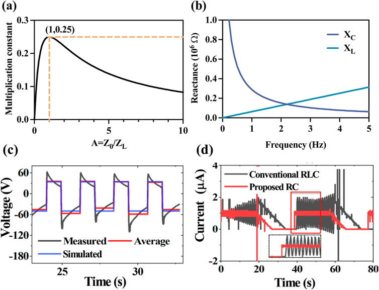
Figure 3. (A) Multiplication constant of
Resonance RLC matching is studied to achieve theoretical maximum power on external load, where the reactance of inductor and capacitor is equal. The relationship of
With a fixed operating frequency of 1 Hz, the empirical formula for capacitor leakage current in Equation 16 states that the constant of current leakage (
To simulate the output of the BEH, its average voltages were calculated and used to generate a pulse signal, shown by the red line in Figure 3C. To enhance the uniformity of the simulated pulse signal, a pulse voltage source with a pulse value of 48 V and a duty ratio of 43% was used for simulation, as shown by the blue line. Figure 3D shows the current ripple elimination through the proposed RC impedance matching. By taking out the inductor from the RLC (which operates in a discontinuous mode) and adding a capacitor for energy storage and filtering, the proposed RC impedance matching enhances the stability of the output. This modification helps prevent capacitor failure and improves the efficiencies of energy transfer and extraction. According to Equations 11–15, the reactance depends on operating frequency, as shown in Figure 3B, with a capacitance of 1 μF and an inductance of 20 kH. When operating under a very low frequency, the
The RC circuit topology design is examined from two specific perspectives, namely, the resistive load (R) and the capacitive load (C), to minimize energy loss and maximize power production. Various permutations and combinations of R and C result in distinct circuit topologies and varying load impedances (
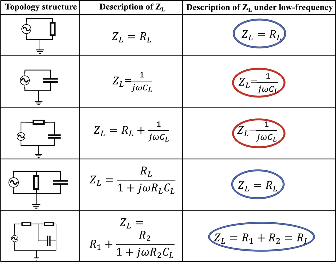
Table 1. Mathematical description of load impedance
Using BEH to power a pure resistive external load, the power output on load can be described as:
Deriving Equation 17 with respect to
The optimum power on external load can be obtained when Equation 18 equals to ‘0’, which occurs at an external load in Equation 19:
Therefore, the
The voltage
Given Equations 20, 21, the voltage and current consistently exhibit a 90° phase delay, resulting in a total energy buildup of zero on the external load during a single operation cycle. This ineffective charging of the external load highlights the need for an AC/DC conversion circuit. Here, we investigated four specific elements of topology modification to improve the PMC based on the pure capacitive load approach.
A full-wave bridge rectifier consisting of four diodes is introduced to convert AC electricity into pulsed DC electricity to avoid energy elimination within one operation cycle. The circuit topology is shown in Figure 4A. Instead of using a commercially assembled rectifier designed for power levels ranging from mW to W, we selected four low-loss diodes to match the BEH’s power level of μW. The energy storage on the capacitive load can be described as:
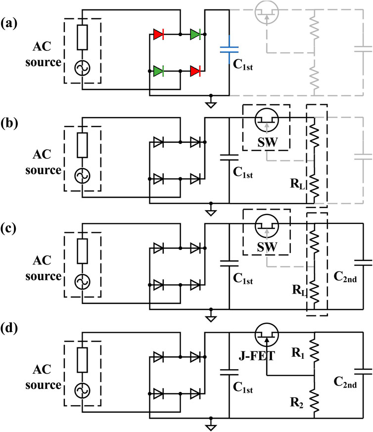
Figure 4. Circuit topologies with (A) AC/DC conversion; (B) RC impedance matching; (C) Second-level capacitor; (D) Switch control.
Deriving from Equations 23, 24, the energy extraction efficiency can be expressed as:
Assuming there is no additional energy loss between the device and the capacitor load. Based on Equation 25, the charge transfer amount is fixed within one operation cycle of the power source, and the efficiency depends on
According to the simulation results with an AC power source of 3 μA and 35 V in Figure 5, an nF-level capacitor demonstrated higher energy extraction efficiency within one operation cycle, particularly with a larger
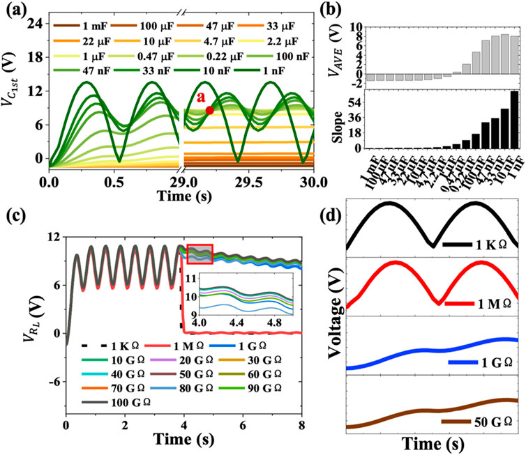
Figure 5. (A) Dependence of voltage accumulation on varying
A switch is used to control the circuit connection between
As demonstrated by the mathematical model, larger capacitance leads to higher energy transfer efficiency over an extended operation period. A
The simulation results of
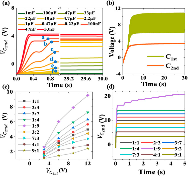
Figure 6. (A) Dependence of voltage accumulation on
The purpose of buck conversion during battery charging in this work is to achieve a safe charging voltage of 3 V. To regulate the voltage, we introduce a J-FET transistor switch, where the voltage division between the gate and drain (
According to the simulation results in Figures 6C, D, the switch can effectively regulate
Recently, a charge excitation circuit (CEC) has been proposed to enhance the device’s surface charge density (Wang et al., 2020; Liu et al., 2019; Liu et al., 2020). However, this topology faces challenges related to potential air breakdown. Unlike CEC, the proposed passive amplification strategy using multiple capacitors enhance charge accumulation and amplifies current without introducing any active components which can cause additional energy consumption. The capacitors are charged in series to fully utilize the output from the BEH, and discharged in parallel to achieve a current amplification with a constant discharging voltage. According to the voltage accumulation results of
In Equations 22, 26,
Experimental validation of
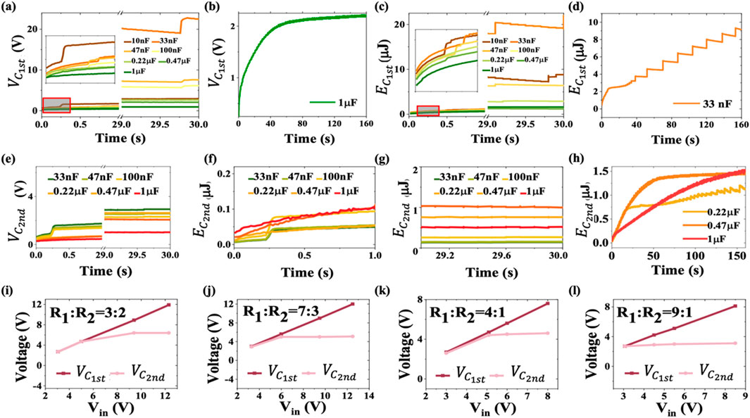
Figure 7. Dependence of voltage accumulation (
Three measuring points (MP_1, MP_2, and MP_3) in Figure 2 were selected. MP_3 measures the voltage on a single capacitor, MP_2 measures the voltage on the two series-connected capacitors, and MP_1 measures the voltage on three series-connected capacitors during the charging of the capacitors. Simulation and experimental results of the three MPs are displayed in Figure 8A, where a stable 3 V is observed across each capacitor. Additionally, processed outputs of Topology_1 and 2 are shown in Figures 8B–D.
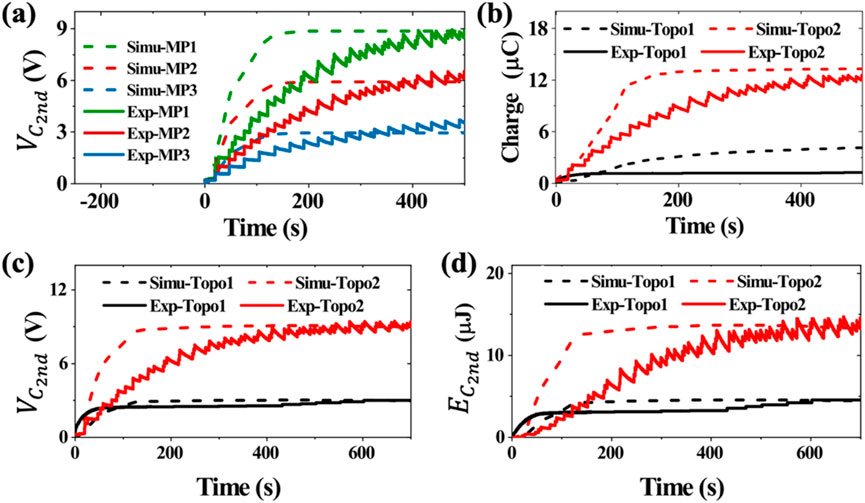
Figure 8. Simulation and experimental results of (A)
In summary, the optimal parameters of the L-PMC Topology_1 are
The energy extraction efficiency refers to the proportion of energy input on loads from the device, which is determined by the PMC matching. The energy extraction efficiency of Topology_1 is compared with other works in Table 2. With a
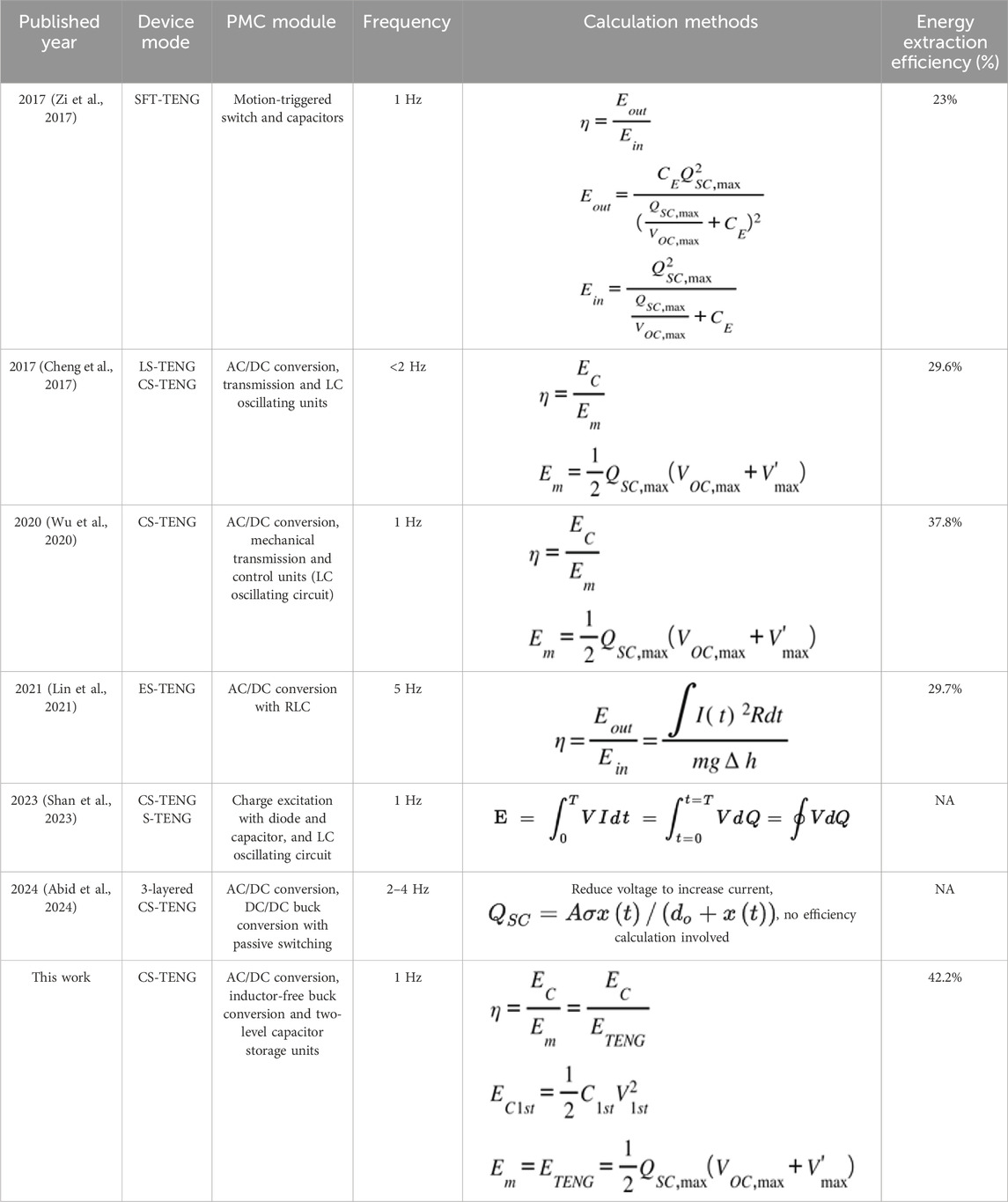
Table 2. Comparison of energy extraction efficiency with published works.
Energy transfer efficiency refers to the proportion of energy stored in the second-level capacitor from the energy input on loads (first-level capacitor), which is calculated as 44.05% based on
While the milliwatt output level of low-frequency biomechanical energy harvesters makes them appropriate for sensing application, their high voltage, weak current, and AC output restrict their effectiveness as a direct power source. Conventional RLC circuit limits the energy transfer efficiency in biomechanical energy harvesters due to the extremely low circuit current. In this study, a low-loss power management circuit is studied with a well-matched 2-stage energy transfer strategy to minimize energy losses, leading to a much higher energy extraction efficiency of 42.24% compared with previous studies. Furthermore, using Topology_1, a battery was charged from 1.9 V to 2.4 V in 10 min with an energy transfer efficiency of 30.59%. The integration of passive current amplification using Topology_2, a 3-fold enhancement in charge accumulation and energy storage is achieved and the energy transfer efficiency achieves an enhancement of 207%. This enables the effective use of the device as DC power source through integration with a battery, demonstrating potential for application in new generation self-powered wearable electronics.
The original contributions presented in the study are included in the article/Supplementary Material, further inquiries can be directed to the corresponding author.
WL: Conceptualization, Investigation, Methodology, Writing–original draft. YH: Methodology, Writing–original draft. CL: Methodology, Writing–original draft, Formal Analysis. AV: Writing–original draft. WD: Conceptualization, Formal Analysis, Funding acquisition, Project administration, Supervision, Writing–review and editing.
The author(s) declare that financial support was received for the research, authorship, and/or publication of this article. This study was supported by the National Natural Science Foundation of China (Grant no. 22072125).
The authors declare that the research was conducted in the absence of any commercial or financial relationships that could be construed as a potential conflict of interest.
The author(s) declared that they were an editorial board member of Frontiers, at the time of submission. This had no impact on the peer review process and the final decision.
All claims expressed in this article are solely those of the authors and do not necessarily represent those of their affiliated organizations, or those of the publisher, the editors and the reviewers. Any product that may be evaluated in this article, or claim that may be made by its manufacturer, is not guaranteed or endorsed by the publisher.
The Supplementary Material for this article can be found online at: https://www.frontiersin.org/articles/10.3389/felec.2025.1501178/full#supplementary-material
Abdelsattar, M., Ismeil, M. A., and Saber Abu-Elwfa, S. (2024). Analysis of renewable energy sources and electrical vehicles integration into microgrid. IEEE Access 12, 66822–66832. doi:10.1109/access.2024.3399124
Abhinav, R., and Pindoriya, N. M. (2016). “Grid integration of wind turbine and battery energy storage system: review and key challenges,” in 2016 IEEE 6th international conference on power systems (ICPS) (IEEE).
Abid, Y., Shuja, A., Ali, M., and Murtaza, I. (2024). Output current boosting in triboelectric nanogenerators for applications in self-powered energy systems. Eng. Sci. Technol. Int. J. 55, 101749. doi:10.1016/j.jestch.2024.101749
Cheng, X., Miao, L., Song, Y., Su, Z., Chen, H., Chen, X., et al. (2017). High efficiency power management and charge boosting strategy for a triboelectric nanogenerator. Nano Energy 38, 438–446. doi:10.1016/j.nanoen.2017.05.063
Faisal, M., Hannan, M. A., Ker, P. J., Hussain, A., Mansor, M. B., and Blaabjerg, F. (2018). Review of energy storage system technologies in microgrid applications: issues and challenges. Ieee Access 6, 35143–35164. doi:10.1109/access.2018.2841407
Fan, F.-R., Tian, Z.-Q., and Wang, Z. L. (2012). Flexible triboelectric generator. Nano energy 1 (2), 328–334. doi:10.1016/j.nanoen.2012.01.004
Fang, C., Tong, T., Bu, T., Cao, Y., Xu, S., Qi, Y., et al. (2020). Overview of power management for triboelectric nanogenerators. Adv. Intell. Syst. 2 (2), 1900129. doi:10.1002/aisy.202070020
Jiang, T., Zhang, L. M., Chen, X., Han, C. B., Tang, W., Zhang, C., et al. (2015). Structural optimization of triboelectric nanogenerator for harvesting water wave energy. ACS nano 9 (12), 12562–12572. doi:10.1021/acsnano.5b06372
Kaper, S. K., and Choudhary, N. K. (2016). “A review of power management and stability issues in microgrid,” in 2016 IEEE 1st international conference on power electronics, intelligent control and energy systems (ICPEICES) (IEEE).
Kong, N., Ha, D. S., Erturk, A., and Inman, D. J. (2010). Resistive impedance matching circuit for piezoelectric energy harvesting. J. Intelligent Material Syst. Struct. 21 (13), 1293–1302. doi:10.1177/1045389x09357971
Lee, K. Y., Chun, J., Lee, J., Kim, K. N., Kang, N., Kim, J., et al. (2014). Hydrophobic sponge structure-based triboelectric nanogenerator. Adv. Mater 26 (29), 5037–5042. doi:10.1002/adma.201401184
Lin, Z., Zhang, B., Xie, Y., Wu, Z., Yang, J., and Wang, Z. L. (2021). Elastic-connection and soft-contact triboelectric nanogenerator with superior durability and efficiency. Adv. Funct. Mater. 31 (40), 2105237. doi:10.1002/adfm.202105237
Liu, W., Wang, Z., Wang, G., Liu, G., Chen, J., Pu, X., et al. (2019). Integrated charge excitation triboelectric nanogenerator. Nat. Commun. 10 (1), 1426. doi:10.1038/s41467-019-09464-8
Liu, Y., Liu, W., Wang, Z., He, W., Tang, Q., Xi, Y., et al. (2020). Quantifying contact status and the air-breakdown model of charge-excitation triboelectric nanogenerators to maximize charge density. Nat. Commun. 11 (1), 1599. doi:10.1038/s41467-020-15368-9
Niu, S., and Wang, Z. L. (2015). Theoretical systems of triboelectric nanogenerators. Nano Energy 14, 161–192. doi:10.1016/j.nanoen.2014.11.034
Niu, S., Zhou, Y. S., Wang, S., Liu, Y., Lin, L., Bando, Y., et al. (2014). Simulation method for optimizing the performance of an integrated triboelectric nanogenerator energy harvesting system. Nano Energy 8, 150–156. doi:10.1016/j.nanoen.2014.05.018
Nouri, T., Hasanpour, S., and Lee, S. S. (2024). A semi-quadratic trans-inverse high step-up DC-DC converter for renewable energy applications. IEEE Trans. Power Electron. 39, 15174–15190. doi:10.1109/tpel.2024.3423666
Shan, C., He, W., Wu, H., Fu, S., Li, K., Liu, A., et al. (2023). Dual mode TENG with self-voltage multiplying circuit for blue energy harvesting and water wave monitoring. Adv. Funct. Mater. 33 (47), 2305768. doi:10.1002/adfm.202305768
Shankaregowda, S. A., Nanjegowda, C. B., Cheng, X. L., Shi, M. Y., Liu, Z. F., and Zhang, H. X. (2016). A flexible and transparent graphene-based triboelectric nanogenerator. IEEE Trans. Nanotechnol. 15 (3), 435–441. doi:10.1109/tnano.2016.2540958
Shi, M., Yang, W., Zhang, Z., Zhao, M., Wang, Z. L., and Lu, X. (2022). Hydrogels with highly concentrated salt solution as electrolytes for solid-state supercapacitors with a suppressed self-discharge rate. J. Mater. Chem. A 10 (6), 2966–2972. doi:10.1039/d1ta08709f
Wang, H., Xu, L., Bai, Y., and Wang, Z. L. (2020). Pumping up the charge density of a triboelectric nanogenerator by charge-shuttling. Nat. Commun. 11 (1), 4203. doi:10.1038/s41467-020-17891-1
Wang, K., Liao, Y., Li, W., Zhang, Y., Zhou, X., Wu, C., et al. (2023). Triboelectric nanogenerator module for circuit design and simulation. Nano Energy 107, 108139. doi:10.1016/j.nanoen.2022.108139
Wang, W. (2019). “Triboelectric nanogenerator: a hope to collect blue energy,” in 2019 4th international conference on control, robotics and cybernetics (CRC) (IEEE).
Wang, X., Niu, S., Yin, Y., Yi, F., You, Z., and Wang, Z. L. (2015). Triboelectric nanogenerator based on fully enclosed rolling spherical structure for harvesting low-frequency water wave energy. Adv. Energy Mater. 5 (24), 1501467. doi:10.1002/aenm.201501467
Wu, C., Wang, A. C., Ding, W., Guo, H., and Wang, Z. L. (2019). Triboelectric nanogenerator: a foundation of the energy for the new era. Adv. Energy Mater. 9 (1), 1802906. doi:10.1002/aenm.201802906
Wu, H., Li, H., and Wang, X. (2020). A high-stability triboelectric nanogenerator with mechanical transmission module and efficient power management system. J. Micromechanics Microengineering 30 (11), 115017. doi:10.1088/1361-6439/abb754
Xu, Y., Zhang, W., Hug, G., Kar, S., and Li, Z. (2014). Cooperative control of distributed energy storage systems in a microgrid. IEEE Trans. smart grid 6 (1), 238–248. doi:10.1109/tsg.2014.2354033
Zhang, H., Chen, Y., Deng, L., Zhu, X., Xu, C., Xie, L., et al. (2024a). Efficient electrical energy conversion strategies from triboelectric nanogenerators to practical applications: a review. Nano Energy 132, 110383. doi:10.1016/j.nanoen.2024.110383
Zhang, Z., Gu, G., Zhang, W., Du, Z., and Cheng, G. (2024b). Triboelectric nanogenerator with enhanced charge density and limited open-circuit voltage for efficient power management and industrial environmental monitoring. Nano Energy 131, 110308. doi:10.1016/j.nanoen.2024.110308
Zhao, Z., Liu, J., Wang, Z., Liu, Z., Zhu, W., Xia, H., et al. (2017). Ultrasensitive triboelectric nanogenerator for weak ambient energy with rational unipolar stacking structure and low-loss power management. Nano Energy 41, 351–358. doi:10.1016/j.nanoen.2017.09.010
Zhou, Y., Zhang, P., Li, J., and Mao, X. (2023). Recent progress of triboelectric nanogenerator-based power management and information processing circuit. Mater. Today Sustain. 23, 100426. doi:10.1016/j.mtsust.2023.100426
Zi, Y., Guo, H., Wang, J., Wen, Z., Li, S., Hu, C., et al. (2017). An inductor-free auto-power-management design built-in triboelectric nanogenerators. Nano Energy 31, 302–310. doi:10.1016/j.nanoen.2016.11.025
Keywords: biomechanical energy harvester, power management, circuit optimization, impedance matching, low-frequency energy storage, energy transfer
Citation: Li W, Huang Y, Liu C, Valencia A and Daoud WA (2025) Low-loss power management strategy for weak and low-frequency biomechanical energy harvesting for new generation wearable electronics. Front. Electron. 6:1501178. doi: 10.3389/felec.2025.1501178
Received: 24 September 2024; Accepted: 15 January 2025;
Published: 14 February 2025.
Edited by:
Amanda S. Koh, University of Alabama, United StatesReviewed by:
Peng Cui, Henan University, ChinaCopyright © 2025 Li, Huang, Liu, Valencia and Daoud. This is an open-access article distributed under the terms of the Creative Commons Attribution License (CC BY). The use, distribution or reproduction in other forums is permitted, provided the original author(s) and the copyright owner(s) are credited and that the original publication in this journal is cited, in accordance with accepted academic practice. No use, distribution or reproduction is permitted which does not comply with these terms.
*Correspondence: Walid A. Daoud, d2Rhb3VkQGNpdHl1LmVkdS5oaw==
Disclaimer: All claims expressed in this article are solely those of the authors and do not necessarily represent those of their affiliated organizations, or those of the publisher, the editors and the reviewers. Any product that may be evaluated in this article or claim that may be made by its manufacturer is not guaranteed or endorsed by the publisher.
Research integrity at Frontiers
Learn more about the work of our research integrity team to safeguard the quality of each article we publish.