 Pallavi Praful
 Chris Bailey
- Electrical Engineering, Arizona State University, Tempe, AZ, United States
Wafer-level packaging (WLP) is a pivotal semiconductor packaging technology that enables heterogeneously integrated advanced semiconductor packages with high-density electrical interconnections through its efficient and highly reliable manufacturing processes. Within this domain, fan-out wafer-level packaging has gained prominence due to its potential for high integration capacity, scalability, and performance on a smaller footprint. This review examines FOWLP technology and its associated challenges, primarily warpage. As semiconductor companies strive to develop cutting-edge packages, wafer warpage remains an intrinsic and persistent issue affecting yield and reliability at both the wafer and package levels. Warpage characterization techniques and modeling approaches, including theoretical, numerical, and emerging artificial intelligence and machine learning (AI/ML) methods, have been analyzed. The structural parameters and properties of the constituent materials of the reconstituted wafer and the FOWLP process have been considered to evaluate the effectiveness of these methods in predicting and analyzing warpage. Potential directions and limitations in warpage prediction and mitigation have been outlined for future research for more reliable and high-performance FOWLP solutions.
1 Introduction
1.1 Advanced semiconductor packaging and heterogeneous integration
In 2015, the International Technology Roadmap for Semiconductors (ITRS), which had served as the premier guide for the semiconductor industry for enabling transistor scaling and progressing Moore’s law for the past 22 years, acknowledged the end of Moore’s law of transistor scaling, signaling a pivotal shift in the semiconductor industry. The report introduced the concepts of “More than Moore” (MtM) for functional diversification improvements and increasing functional density through heterogeneous integration of diverse digital and non-digtal components at the semiconductor package level (Gargini, 2015). A semiconductor package is a protective casing that contains one or more discrete semiconductor devices or integrated circuits (ICs), providing a means to connect internal components to external circuitry and thermal management structures, and protect them from contamination. In 2019, the first version of the heterogeneous integration roadmap was published with a strong focus on integration, packaging, testing, and interconnect technology required to meet the needs of advanced technologies such as AI and high-performance computing (HPC) (Chen and Bottoms, 2019).
The semiconductor manufacturing ecosystem comprises two main phases: front-end and back-end. The front-end phase focuses on the fabrication of integrated circuits on semiconductor substrates, while the back-end phase encompasses the testing, packaging, and electrical connectivity of these IC substrates.
Established manufacturing processes and their cost-effectiveness have contributed to the widespread adoption of traditional leadframe and substrate packages, such as Dual-in-Line (DIP), Ball Grid Array (BGA), and Quad Flat No-Leads (QFN) packages, to name a few. Outsourced Semiconductor Assembly and Test (OSAT) companies at the back-end-of-line (BEOL) have handled packaging for decades, primarily optimizing for labor costs and manufacturing simplicity without fully considering the potential for technological advancements. However, as ICs have grown increasingly complex and transistor scaling has approached its physical limits, heterogeneous integration and advanced packaging has emerged as a solution. The demand for compact, high-performance, and cost-effective electronic devices in the consumer electronics market over the past decade has been primarily addressed through System-on-Chip technology. System-on-chip (SoC) is an integrated circuit design that combines numerous or all the high-level functional components of an electronic device onto a single chip, rather than the traditional method of employing separate components mounted on a motherboard or printed circuit board (PCB). However, these monolithic structures can no longer meet the physical and cost demands of emerging applications. As a result, heterogeneous integration (HI) and advanced packaging have become indispensable in addressing the need for high-density system integration by utilizing the System-in-Package (SiP) approach, wherein multiple chips with diverse functionalities are contained within a single package. Figure 1 illustrates an example of advanced packaging, where multiple dies are integrated onto a substrate and mounted on a PCB.
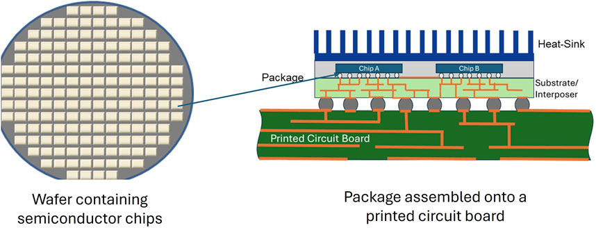
Figure 1. Dies integrated within an advanced semiconductor package.
Advanced packaging technologies enable HI by allowing the integration of various chips from different manufacturing technologies, wafers, or even foundries into a single package, offering improved performance, power efficiency, and functionality with new technologies such as 2.5D and 3D integration (Wesling, 2020; Chen and Bottoms, 2017). 2.5D and 3D refer to different levels of integration and stacking of chips within the same package. Typically, chips are packaged individually and mounted on a printed circuit board (PCB). In 2.5D packages, chips are placed side-by-side on an interposer or substrate. Substrates can be made of organic or ceramic materials, whereas interposers are made of silicon, enabling high-density interconnections between the chips. These silicon interposers are produced using chip fabrication processes. In 3D advanced packages, multiple chips are vertically stacked and connected with through-silicon vias (TSVs). TSVs offer high bandwidth and low latency for applications such as high-performance computing and artificial intelligence. Figure 2 illustrates examples of 2.5D and 3D packaging architectures.
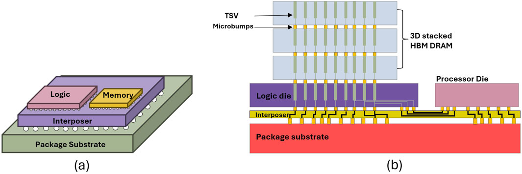
Figure 2. (A) 2.5D semiconductor package strucutre (B) 3D integration of memory, logic and processor dies within a package.
The key end applications driving the adoption of advanced packaging technologies are:
1. Autonomous driving
2. Artificial intelligence
3. Consumer electronics
4. Communication and networking infrastrucure
5. High-performance computing
6. Internet of Things (McKinsey & Company, 2025)
Top semiconductor foundries like TSMC, Samsung, and Intel, as well as OSATs such as ASE and Amkor, seek to expand their presence in the advanced semiconductor packaging market as the technology becomes increasingly complex and profitable.
1.2 Wafer-level packaging
Wafer-level packaging (WLP) is a prominent advanced semiconductor packaging technique in which integrated circuits and other components are packaged while still on the wafer. This approach significantly reduces manufacturing costs and improves yields by performing packaging operations on entire wafers. WLP enables the creation of smaller package sizes with enhanced electrical performance, addressing the demand for more compact and efficient electronic devices (Liu et al., 2014). Its scalability and integration capabilities support advanced system-in-package systems and improve package reliability through improved process control (Liu et al., 2014). Furthermore, WLP’s compatibility with existing semiconductor manufacturing processes eases its implementation in current facilities. With WLP, wafer-based processing, and front-end fabrication equipment such as using lithography tools can be adapted for creating redistribution layers (RDL). WLP also streamlines back-end processes by reducing assembly steps and enabling efficient wafer-level testing. WLP is an attractive option for various semiconductor applications, particularly in industries where size, performance, and cost are critical factors (Lau, 2018).
1.3 Fan-out wafer-level packaging
One of the latest advances in wafer-level packaging is fan-out wafer-level packaging technology (FOWLP). This approach involves placing dies from different wafers onto a reconstituted wafer and redistributing the interconnects on the wafer, enabling a greater number of input/output connections compared to traditional chip-scale packaging. Fan-out wafer-level packaging also offers other benefits, such as reduced form factor and the ability to integrate multiple passive and active components within a single package. Figure 3 highlights the key differences between traditional packaging, wafer-level packaging, and fan-out wafer-level packaging. In traditional packaging, dies are diced from a silicon wafer and then packaged individually. In contrast, wafer-level packaging involves packaging the dies while they remain on the wafer. FOWLP places the dies onto a temporary carrier wafer, performs molding and other packaging processes, and then proceeds with package singulation.
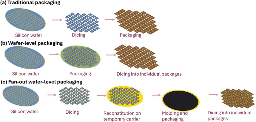
Figure 3. (A) Traditional packaging process (B) Wafer-level packaging process (C) Fan-out wafer-level packaging process.
Furthermore, FOWLP technology can be used in Multi-Chip-Module (MCM) packages that simply integrate chips of different types and sizes into a module or subsystem, or in System-in-Package (SiP) applications that combine diverse chips into a single system. For mid-to high-end device integration requirements in consumer and high-performance computing (HPC) applications, which might typically require an expensive 2.5D interposer with through-silicon vias (TSV), fan-out technology offers a cost-effective alternative (Lim and Wee, 2018). 3D fan-out Package-on-Package (PoP) solutions utilize electrical routing through redistribution layers (RDL) on both the top and bottom faces of packages (see Figure 4) (Sandstrom et al., 2021). Combined with through-mold or through-package vias for communication between packages in the 3D stack, the PoP strucutre enables thinner profiles and smaller footprints on a printed circuit board (PCB). These through mold-vias can also be used for thermal management (Lau and Yue, 2009).
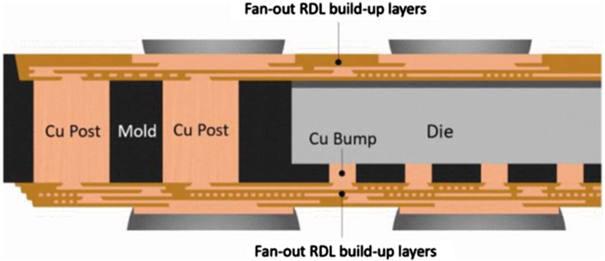
Figure 4. Fan-out RDL layers on top and bottom faces of a Deca M-SeriesTM3D PoP (Sandstrom et al., 2021). Reprinted with permission from IEEE Proceedings.
The other type of wafer-level packaging is the fan-in wafer-level packaging or wafer-level chip-scale packaging (WLCSP), typically used for low-end mobile devices with basic technological requirements and lower I/O requirements, and the redistribution layers are routed toward the center of the die. In contrast, fan-out wafer-level packaging features RDLs and solder balls that exceed the size of the die, allowing the chip to have more input/output connections while maintaining a thin profile.
A key driver for fan-out technology has been the need for higher I/O densities and finer RDL with line-space (L/S) measurements (‘line’ refers to the width of the metal trace, while ‘space’ refers to the gap between adjacent traces). Fan-out packaging is further divided into three subtypes based on I/O densities and L/S: core, high density, and ultra-high density.
1. Core fan-out packaging with
2. High density fan-out packaging with 6
3. Ultra high density (UHD) FO packaging with
Fan-out technology was first developed at Infineon between 2001 and 2007 with the creation of the embedded wafer-level BGA (eWLB). The eWLB was subsequently licensed by Infineon to other Outsourced Semiconductor Assembly and Test (OSAT) companies, including ASE, Amkor Portugal, JCET Group, and STMicroelectronics, for manufacturing their own line of products. In 2016, wafer-level fan-out packaging gained significant attention when Taiwan Semiconductor Manufacturing Company (TSMC) announced the use of their fan-out (FO) product, Integrated Fan-Out (InFO), to package the application processor engines (APE) for Apple’s iPhone 7. Since then, Apple has become the largest original equipment manufacturer (OEM) to be the largest consumer of FO technology. TSMC is the largest supplier of FO in the world and has continued to expand its FOWLP offerings, developing derivatives such as InFO AiP (Antenna in Package) and InFO PoP (Package in Package) to cater to the networking and high-performance markets (Keser and Kröhnert, 2019).
Future development in FOWLP is to fabricate more RDL layers on the wafer to accommodate greater I/O, which necessitates finer line/spacing
Deca developed the unique M series FOWLP in 2012 that employs their proprietary Adaptive Patterning™, enabling high-density integration and improved yields for multichip modules (Bishop et al., 2016). The Deca M-series features a fully encapsulated structure and a proprietary planarized surface with a molded stress buffer layer over the active device surface. The M-Series offers multiple variants such as multi-die packaging, chiplet integration, 3D PoP, and embedded bridge die interposers. With 3D configuration capabilities, embedded components, and fine-pitch connections on both sides of an organic interposer, the M-Series has been adpated for high-performance applications such as AI and HPC.
2 Fan-out wafer-level packaging process flow
2.1 FOWLP packaging approaches
Classical wafer-level packaging process begins with wafer preparation, including back grinding and dicing operations. Redistribution layers are created through dielectric application and copper plating. Photolithography, sputtering, and electroplating are used to form the desired patterns and metal layers. After photoresist stripping and metal etching, a dielectric layer is applied as a protective coating. Solder balls are then attached, followed by electrical testing and final wafer dicing. FOWLP distinguishes itself from conventional wafer-level packaging with the reconstitution process, where the fan-out region is developed over a molded wafer (also called a reconstituted wafer). Different fan-out approaches, such as chip-first die face-down and die face-up, and chip-last or RDL-first as shown in Figure 5, have evolved to address diverse application requirements and overcome manufacturing limitations (Lau, 2022).
1. Chip-first die face-down: Known good dies (KGDs), singulated from the device wafer, are attached face-down to a temporary wafer with a thermal release tape. After compression molding with liquid EMC to encapsulate the silicon die and post-mold cure (PMC), the temporary wafer is removed with a thermal debonding step. Redistribution layers (RDLs) for electrical signal routing are built on the backside of the exposed dies. Solder balls are then mounted over designated spots on the RDL layer to establish connection between the chip package and an external printed circuit boards (PCB) before reconstitued wafer is singulated into individual package entites.
2. Chip-first die face-up: On the origial device wafer, copper studs are prefabricated using electroplating. These dies are then assembled using a high-speed pick-and-place tool on a reconstituted wafer. The wafer is then molded with compression molding and cured. The EMC at the top of the wafer is backgrinded to expose the copper studs, and RDL layers are developed.
3. Chip last or RDL first: RDL layers are first fabricated on the reconstituted wafer. The KGDs of the original device wafers are then placed on top of the reconstituted wafer with RDL. Compression molding is performed next, followed by backgrinding and debonding from the temporary wafer carrier. Solder balls are mounted and the wafer is singulated into individual packages.
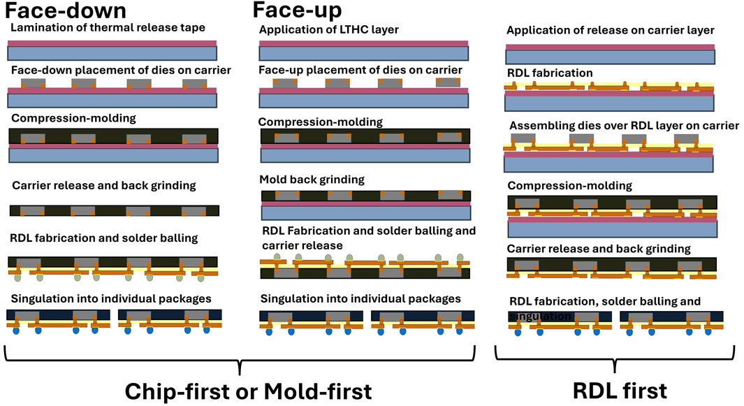
Figure 5. Fan-out packaging approaches.
Although wafer-level packaging has an established infrastructure, the industry is also transitioning to panel-level packaging primarily due to cost reduction and increased productivity. Panel-level packaging can reduce costs by more than 20%, especially for larger package sizes, by using rectangular panels that offer more space. This approach achieves up to 95% area usage compared to 85 for round wafers, allowing for more packages per carrier and reduced handling time. Adopting panel-level fan-out packaging could enable higher throughput, better area utilization, lower costs, and scalability (Braun et al., 2019; Lau et al., 2020; Braun et al., 2021; Braun et al., 2018).
2.2 Warpage evolution in FOWLP process flow
The fan-out wafer-level packaging process involves multiple temperature excursions and pressure conditions, which can induce different stress states and lead to warpage at the wafer and package levels (Lau et al., 2018a; Lau al., 2018b). Fundamentally, warpage is an out-of-plane deformation. The FOWLP manufacturing line must follow a rigorous sequential process to maintain uninterrupted production and maximize yield. Warpage can disrupt the manufacturing process, making it difficult for various equipment to handle deformed wafers. Wafers with coplanarity issues may also face misalignment during RDL build-up, ball placement, and wafer singulation processes, leading to degradation in the reliability of the final packages or even delamination and breakage of the wafer (Chen et al., 2022).
Deca’s M-Series employs a unique chip-first face-up approach to FOWLP that has drawn considerable attention in the industry due to its high yield and reliability (Shoo et al., 2019). To understand the evolution of warpage in one of the latest FOWLP manufacturing processes, the Deca M series process can be examined as an exemplary as shown in Figure 6 (Rogers et al., 2017).
1. Wafer preparartion: This step includes the fabrication of copper studs on the device wafer. The seed layers are sputtered and a thick photoresist is patterned. Copper studs are electroplated over the under bump metallization (UBM), stripping and etching the photresist and seed layers. The top of the device wafer is coated with a polymer, and its bottom side is laminated with a die-attach film (DAF). The wafer is singulated into individual chips.
2. EMC Molding and Curing: The dies are aligned with their active side face-up precisely on a reusable temporary carrier at designated fan-out pitches. EMC is dispensed over the reconstituted carrier wafer and compression molding is performed in a mold cavity to encapsulate all components on the carrier under timed pressure and temperature conditions. After the initial molding process (in-mold cure or IMC) to solidify the viscous EMC, a post-mold cure (PMC) step at temperatures higher than those of IMC is required to complete the curing and stabilize the EMC. The cured carrier is then cooled to room temperature.
Figure 6. Deca’s M-series chip-first process flow for a fully molded FOWLP. Reprinted with permission from IEEE Proceedings (Sandstrom et al., 2021).
The first significant warpage occurs after the post-mold cure process. This warpage is primarily attributed to the mismatch in coefficient of thermal expansion within the die-mold-carrier assembly stack, as well as the evolving properties of the encapsulating EMC (Lau, 2018).
This carrier is detached from the carrier from the reconstituted wafer through a debonding step. The warpage of the reconstituted wafer is significantly increased during the debonding process, as the stresses accumulated in the wafer are suddenly released and redistributed (Lin et al., 2016; Lim et al., 2018). EMC molding is removed using a backgrinding machine to reveal the Cu contact pads over which RDL layers will be developed. The backgrinding process can induce mechanical stresses that impact wafer warpage.
Optical scanning is later used to record the location of every die on the reconstituted wafer.
3. RDL fabrication: This stage includes curing and patterning of dielectric polymer to provide insulation between copper traces in the RDL layer. The Cu RDL layers are then patterned and electroplated over the exposed Cu studs’ surfaces to reroute the die’s input/output (I/O) connections from their original locations to new positions in the package area.
The differences in Young’s modulus and coefficient of thermal expansion between the photosensitive polyimide and copper traces create an uneven stress distribution across the assembly, leading to warpage.
Flux is applied to the solder ball attachment areas, and the solder balls are then mounted through the solder reflow process. The peak temperature reached during this reflow step is 200°.
The reflow process introduces thermal stress due to temperature changes, aggravating warpage from CTE mismatches. Additionally, the mounting process itself can introduce new stresses and deformations, potentially altering the package’s post-manufacturing warpage characteristics.
4. Package finishing: In the last step, backgrinding is performed to thin the package and the packages are singulated.
Warpage, die-shift and RDL processing are closely interrelated. Warpage in the reconstituted wafer can directly cause die shift, as the distorted wafer surface may disrupt the alignment of dies placed on the carrier. Excessive warpage also hinders lithography tools from correctly patterning RDL traces on the wafer or panel. RDL fabrication relies on high-precision photolithography to pattern fine interconnects between chips. If the wafer has warped or the dies have shifted, the RDL layers may not align correctly with the underlying dies, leading to faulty or incomplete connections. Warpage can also cause variation in layer thickness, which impacts electrical performance and increases the risk of shorts or open circuits. Thus, improved warpage management and die shift control can ease the RDL patterning process. To achieve these goals, process control plays a critical role across all areas of semiconductor manufacturing, enabling high yields and better profit margins (Lu, 2018).
3 Measuring warpage
The Semiconductor Equipment and Materials International (SEMI) organization characterizes the warpage of wafers with respect to the orientation of its functional surface. When viewed from the functional surface as depicted in Figure 7, if the center is depressed and the edges protrude upward concavely, this constitutes a positive warpage value (smiling face). In contrast, a negative value (crying face) is indicated by a convex shape with the center protruding and the edges depressed downwards.
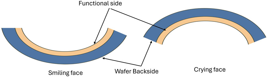
Figure 7. Definition of warpage orientation.
Temperature-dependent warpage can be measured with non-contact moiré-based methods such as thermal shadow moiré and digital fringe projection (DFP). Digital image correlation (DIC) is a non-contact, stereo-vision based method that can capture dynamic warpage behaviour. While there are several moiré-based techniques available, including shadow moiré, laser fringe projection, and digital fringe projection, and other non-contact techniques this discussion will focus specifically on shadow moiré, DFP, and DIC as these methods seem to be the most widely adopted metrology tools for wafer warpage (Sun and Zhang, 2024).
3.1 Moiré-based measurement
Moiré-based optical methods measure surface deformations and displacements by analyzing interference patterns, called moiré fringes, created by the superimposition of two similar patterns.
Shadow Moiré is a relatively simple optical technique used to measure out-of-plane deformations and surface profiles by analyzing moiré fringes generated by a diffused light source and a reference grating. A CCD (Charge-Coupled Device) camera, captures images of these fringes (see Figure 8), which are then processed to reconstruct the out-of-plane topography of the surface, as shown in Figure 9. The sensitivity and resolution of the measurement are primarily controlled by the pitch (line spacing) of the reference grating, with finer gratings generally providing higher sensitivity. Shadow Moiré offers advantages such as full-field measurement capability, dynamic real-time display of deformations, and a simpler setup compared to other optical measurement methods (Sun and Zhang, 2024).
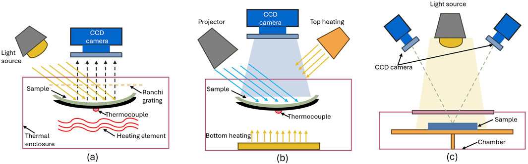
Figure 8. (A) Shadow Moiré setup (B) Digital fringe projection Setup Set (C) DIC setup.
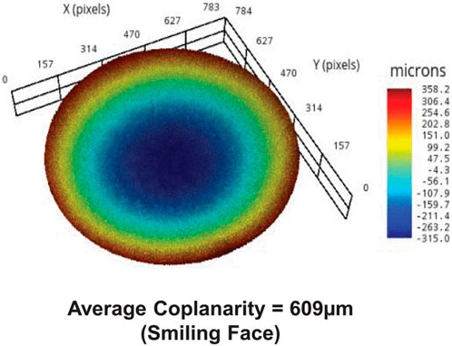
Figure 9. Shadow moiré warpage measurement of reconstituted wafer. Reprinted with permission from IEEE Transactions on Components, Packaging and Manufacturing Technology (Lau et al. 2018b).
Digital fringe projection involves projecting fringes at an angle onto a sample, as shown in Figure 8, which are then captured by a camera. The system also records the phase information of the fringes at each point as the sample’s surface topography changes. DFP leverages these phase data to generate high-resolution 3D representations of a wide range of surfaces, enabling the measurement of both in-plane and out-of-plane deformations. However, DFP tools require a calibration process that could potentially affect the quality of sample measurement (Hubble and Weaver, 2017).
Both shadow moiré and DFP have quick data acquisition capabilities, provide sub-mil or more resolution, and heating chambers with fast temperature ramping for dynamic warpage measurement; shadow moiré provides only single-sided heating that can lead to non-uniform heating of the sample, whereas DFP can uniformly heat both sides (Hubble and Weaver, 2017).
3.2 Digital image correlation
Digital image correlation (DIC) is a stereo vision-based optical technique used to measure full-field displacements and strains on material surfaces by tracking the movement of a random speckle pattern applied to the specimen as the material deforms. A basic DIC setup includes one camera for 2D measurements or two cameras for 3D measurements, lenses, lighting, a speckle pattern on the specimen surface, and DIC software for image processing and analysis (see Figure 8) (Sutton and Hild, 2015).
DIC measurements require speckle patterns that display high contrast, random features, proper deformation with the specimen surface, and appropriate sizing for the field of view and resolution. These speckle patterns are typically applied using techniques such as spray paint, airbrush, stencils, or toner powder, and the quality of their application affects measurement accuracy. Advanced image processing algorithms track the deformation of the speckle pattern between images with subpixel accuracy, allowing DIC to achieve high measurement precision (Sun and Zhang, 2024).
While extensive sample preparation and reliance on computer algorithms for good measurement results present challenges, DIC offers unique advantages such as high-throughput measurement of coefficient of thermal expansion (CTE) and real-time, in-situ measurements during processes like solder reflow for packages. Additionally, DIC experimental data can be linked with CAD tools and finite element analysis (FEA) simulations. Loading histories and boundary conditions of DIC experiments can be monitored and applied to FEA software for simulation accuracy. DIC experimental results can be compared to FEA predictions in CAD environments (Sutton and Hild, 2015).
While shadow moire, DFP and DIC are noncontact full-field metrology tools for warpage, the choice for a particular experiment depends on specific requirements such as the need for in situ measurements, surface characteristics of the wafer, and the type of deformation (out-of-plane only or both in-plane and out-of-plane).
3.3 Critical warpage thresholds and their impact on manufacturing yield
The warpage thresholds for a 300 mm reconstituted wafer is 1 mm, beyond which handling and subsequent process integration become challenging, affecting the manufacturability and reliability of the final devices. For high yields, warpage should be less than 0.5 mm (Lau, 2019b). The maximum allowable warpage of an individual package is recommended to be 0.2 mm, but 0.1 mm is preferred for high yield (Lau et al., 2018b).
4 Modelling warpage
Experimental, analytical, and numerical methods are essential to predict and control warpage in wafer-/panel-level fan-out manufacturing, considering the complex interplay of constituent material properties, structural and geometric parameters, and process dependencies.
4.1 Material data for warpage analysis and modelling
Warpage modeling approaches are intrinsically dependent on extensive material characterization to ensure accuracy and reliability in their results. Compression molding is one of the initial stages where considerable warpage is observed, and this warpage is attributed to the temperature and cure-dependent behavior of the EMC. As a result, characterizing the material properties of the EMC is a key step in warpage analysis, and assuming simple elastic properties for the EMC can overestimate warpage, as demonstrated in Figure 10.
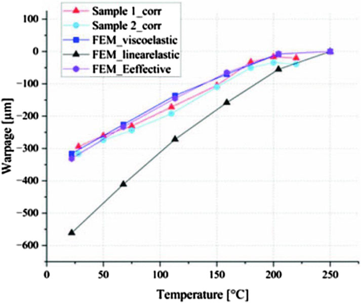
Figure 10. Comparison of experimental results to viscoelastic and effective elastic FEM model. Reprinted with permission from IEEE Proceedings (Huber et al., 2024).
4.1.1 EMC material properties
1. Estimation of chemical shrinkage and coefficient of thermal expansion of EMC: The EMC is a composite material with epoxy resin as a matrix and silica particles as a filler. As the temperature increases during mold curing and post-curing processes (typically 130°C–175°C), the polymers in the EMC cross-link and solidify, causing a volumetric shrinkage known as chemical shrinkage (Phansalkar et al., 2022). As the EMC cures, it contracts, causing volume reduction and generating internal stresses. This process leads to nonuniform shrinkage across the package, creating asymmetric stress distribution and localized strain. Volumetric shrinkage occurring due to CTE mismatches throughout the entire molding and cooling process and are referred to as thermal shrinkages (Tan et al., 2013). Chemical aging is another phenomenon where continued crosslinking occurs in some reactive sites even after initial curing, which can also result in volume shrinkage (Chiu et al., 2011). The chemical shrinkage of the EMC due to polymerization can be estimated by characterization of cure kinetics of the EMC. The degree of conversion (DOC), denoted as α, quantifies the extent of cross-linking and the formation of a 3D polymer network. It reflects the progress of the curing reaction toward the fully cured state, as shown in Equation 1 (Chiu et al., 2011):
where
where
a. Reaction order (
b. Rate constants (
c. Activation energy
These parameters are obtained by fitting the model to experimental DSC data. Kamal’s model provides information on how the curing reaction progresses over time and temperature. This data can be used to estimate the evolution of chemical shrinkage throughout the curing process. The conversion rate verus time can be estimated and chemical shrinkage of EMC in its fully cured state can be used in process-dependent modeling for warpage prediction using an initial strain approach (Cheng and Liu, 2019; Cheng et al., 2020; Yeh et al., 2015).
Another method for estimating cure-induced volumetric shrinkage is the P-V-T-C equations. The PVTC equation can be simply expressed as polynomials to describe the historical profiles of volume shrinkage under specified isothermal and isobaric states. PVTC equations describe how the specific volume of the EMC changes as a function of pressure, temperature, and degree of cure during the molding and curing processes. This allows accurate modeling of both the thermal and chemical shrinkage of the EMC during molding (Hong and Hwang, 2004; Chang et al., 2002).
Thermal mechanical analysis (TMA) instruments can characterize the chemical shrinkage of the epoxy molding compound during polymerization conversion and chemical aging. In the TMA method, the coefficient of thermal expansion is measured in-plane and out-of-plane over time and temperature (Chiu et al., 2011; Cheng and Liu, 2019).
2. Cure-dependent viscoelastic nature of EMC: The EMC exhibits time and temperature-dependent viscoelastic behavior during the curing process. The stresses that develop in the EMC do not immediately dissipate but gradually relax over time. The Prony series can effectively capture the time-dependent nature of the viscoelastic EMC, providing a good approximation of the relaxation Young’s modulus (Yeh et al., 2015). This is a master function given by Equation 3 for the viscoelastic material in time domain can be described by using the generalized Maxwell spring-dashpot model. Prony series coefficients can be determined from experimental data obtained through dynamic mechanical analysis (DMA). The DMA method can be used to measure the relaxation Young’s modulus of the substrate, mold compound, and underfill. Young’s modulus is measured by applying a cyclical load at the centre of the sample in a temperature-controlled environment.
where
The Prony series parameters are input into the FEM software to define the viscoelastic material behavior. This allows the simulation to account for time-dependent stress relaxation and creep during the wafer packaging process. When combined with time-temperature superposition principles, Prony series can effectively model the temperature-dependent response of EMC during thermal cycles in wafer packaging process. The material properties of the EMC are strongly influenced by its glass transition temperature,
where
4.2 Analytical models to simulate residual stresses
4.2.1 Stoney’s equations
In 1909, George Stoney investigated the deformation of a steel rule (substrate) with a thin metal film deposited on it through electrolysis. His research laid the groundwork for the famous Stoney equation, shown in Equation 5, which describes the relationship between the stress in the deposited film and the resulting curvature of the substrate (Stoney, 1909):
where
where d is the wafer diameter, and R is the radius of curvature of the deformed wafer.
This adaptation made it widely applicable in the semiconductor manufacturing industry for analyzing wafer warpage. FEM models often use Stoney’s equation as a reference point, with researchers comparing FEM results to Stoney’s predictions to validate their models or highlight improvements (Schicker et al., 2016). The Stoney equation has limited applicability as it is only valid for cases where the substrate and film materials exhibit isotropic linear elastic behavior, the film thickness is significantly smaller than the substrate thickness, and the radius of curvature is much greater than the substrate thickness. Several studies have attempted to extend the scope of the Stoney formula by proposing modified versions that relax the assumptions of isotropic substrate materials (Janssen et al., 2008), the film thickness being much smaller compared to the substrate (Injeti and Annabattula, 2015), and the uniform film stress distribution (Qiang et al., 2021). Due to the involvement of different materials and complex geometries in heterogeneously integrated wafer assemblies, Stoney’s equation becomes inadequate. It does not account for non-uniform stress distributions, non-linear material behavior, complex geometries, and multiple layers with varying properties (Ostrowicki et al., 2018).
4.2.2 Timoshenko’s theory for bilayer materials
Timoshenko’s analytical solutions for bi-material layers have been employed to investigate the CTE mismatch stresses in the multi-material layers of the wafer assembly. This approach enables a quick and reliable prediction of warpage in the reconstituted wafer (?) (Vellukunnel et al., 2023; Xing et al., 2015).
In a bilayer strip, a mechanical displacement occurs as a result of thermal changes within the interface as shown in Figure 11. Timoshenko’s analysis provides a curvature and maximum deflection for this deformation as shown in Equations 7, 8 respectively (Vellukunnel et al., 2023):
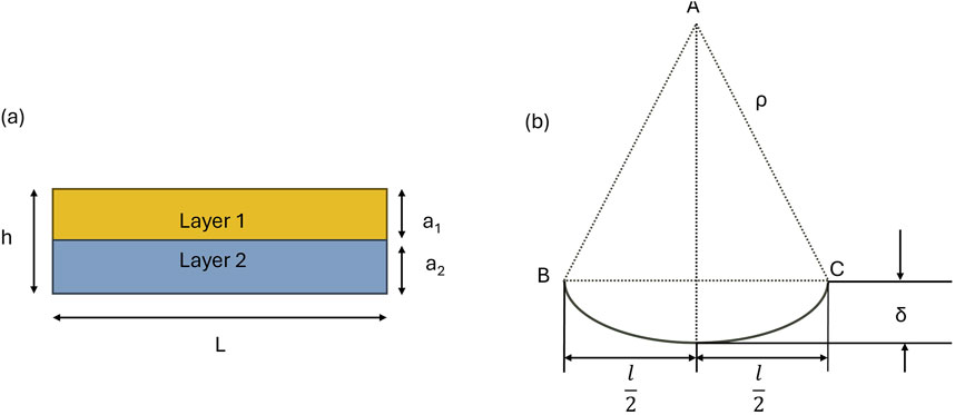
Figure 11. (A) Bilayer strip (B) Deflection of bilayer strip.
where
Effective material propertives of Young’s modulus and CTE can be used to accurately represent multi-component layers for curvature estimation with Timoshenko’s equations (Xing et al., 2015).
4.3 Numerical modelling approaches
FEM has been crucial in studying how different properties of the material affect the warpage and stress distribution. Multiphysics finite element modeling enables the simulation of coupled thermomechanical effects, accounting for both thermal stresses and mechanical deformations simultaneously.
FEM can incorporate nonlinear material behaviors, temperature-dependent properties, and viscoelastic effects, providing a more realistic representation of material responses. The viscoelastic properties of EMC play a crucial role in warpage behavior, especially at high temperatures. The functional group cross-linking reaction of EMC and its viscoelastic relaxation contribute to warpage during the reconstituted wafer process.
4.3.1 Process-dependent modeling methodology
FEM models can characterize the evolution of the warpage during a single or all processes by using process-dependent modeling methodologies. The warpage orientations of the reconstituted wafer can evolve from convex to concave bow shapes during the different processes of fan-out packaging, as shown in Figure 12. Process modeling techniques primarily involve a thorough investigation of the temperature profiles in a real fan-out fabrication process. FEM models combine thermal and mechanical responses to represent the evolution of warpage induced by these temperature profiles. Coupled chemical-thermomechanical FEM models in which the cure kinetics and the cure-dependent viscoelastic behavior of EMC material have proven effective in this regard (Cheng et al., 2020; Yeh et al., 2015; Chiu et al., 2018).
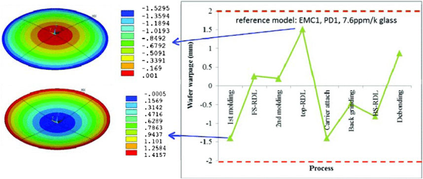
Figure 12. Simulation of warpage trend during Fan-out manufacturing. Reprinted with permission from IEEE Proceedings (Chong et al., 2020).
ANSYS’s element birth-and-death technique is a powerful approach used to model various stages of the FOWLP manufacturing process sequentially. This method selectively activates and deactivates different elements within the finite element model, accurately representing the different layers and materials involved. By manipulating the inclusion of elements such as the epoxy molding compound, carrier wafer, redistribution layers, and debonding materials, engineers can effectively model crucial stages such as compression molding, debonding, back grinding, and RDL fabrication. For example, during the simulation of the molding process, only the EMC layer and the carrier are active, while other components remain inactive. Back grinding can be modeled by deactivating certain parts of the EMC layer, simulating the removal of excess material. As RDL layers are created, their corresponding elements are activated in sequence, mimicking the build-up process. This technique provides valuable insight into thermal management and potential reliability issues throughout the FOWLP manufacturing sequence. Proper selection of elements and consideration of residual stresses from previous stages are crucial to a accurate representation of the physical process. Validating the model with experimental data at key stages helps ensure accuracy, enabling engineers to gain insight into the FOWLP process and optimize process and material properties (Xing et al., 2015; Cheng and Liu, 2019; Wu and Lan, 2019).
The nonaxisymmetric or asymmetric warpage behavior of reconstituted wafers can be modeled by incorporating nonlinear finite element analysis and the impact of gravity in process-dependent FEM simulations (Cheng and Liu, 2019; Cheng et al., 2020).
Coupled explicit dynamic and static models can address transient and steady-state events during the fan-out process, such as grinding on the backside where the excess EMC is removed by a grinding wheel to reduce overall package thickness and weight. Wafer stiffness is often unable to support grinding stress on the surface and warpage can occur. To analyze the grinding stress on silicon wafers during the back-side grinding process, a finite element model is established by setting dynamic loads and contact conditions. An explicit dynamic model is used to simulate the relationship between the grinding wheel and the silicon wafer. A static model is incorporated with the explicit dynamic model to predict the wafer warpage grinding stress on the damaged layer of the silicon wafer. This method provides valuable information regarding the grinding wheel rotation speed, the wafer rotation speed, and the feed rate effectively control the wafer warpage (Wu et al., 2023; Wu and Wong, 2024).
4.3.2 Material representation through homogenization methods
Fabrication of RDL layers involving PI passivation and electroplating of copper layers can induce warpage. Each step in the RDL fabrication process, including deposition, patterning, and curing of the dielectric and metal layers, introduces stress into the wafer structure. Warpage is primarily caused by mismatches in the thermal expansion coefficient (CTE) between the deposited materials, with electrochemically deposited Cu traces substantially contributing to the total warpage due to the CTE mismatch and plastic deformation (Zhu et al., 2014). The high aspect ratios of the Cu traces in the RDL layers can face issue meshing in FEM software. To simplify modeling of complex Cu traces, pads, vias, and dielectric layers, we approximated these layers as equivalent homogeneous medium and evaluated their effective properties. Trace mapping methods have also been used to simplify cu traces in packages.
Homogenization techniques have been applied to approximate the complex layout of redistribution layers, which consist of a mixture of copper and polyimide in varying proportions on a carrier substrate in the RDL-first approach. Rule of mixtures has been employed to determine the effective properties, such as the elastic modulus and the coefficient of thermal expansion, of the RDL layers comprising both copper and PI. This approach helps to account for the influence of these constituent materials on the overall warpage behavior (Huber et al., 2024).
4.3.3 Parametric analysis
Parametric analysis in conjunction with Finite Element Method (FEM) has been extensively used to understand dominating factors and process conditions for wafer warpage simulation in FOWLP. This approach involves systematically varying key parameters such as material properties (e.g., viscoelastic properties of Epoxy Molding Compound and Polyimide) (Hu et al., 2023; Hamaguchi et al., 2016), geometric dimensions (e.g., die size and thickness) (Hu Z. et al., 2021; Wu and Lan, 2019), and process conditions (e.g., temperature profiles during curing) (Sanchez et al., 2022). These studies have provided valuable information on the factors that influence warpage, enabling quantitative relationships to be established between various parameters and warpage outcomes. This methodology has proven crucial for the optimization of the design, sensitivity analysis, and process improvement in FOWLP, ultimately guiding material selection and fabrication processes to minimize warpage in semiconductor packaging.
4.3.4 AI/ML models
Recent research has explored artificial intelligence and machine learning approaches to predict warpage in fan-out wafer-level packaging. The complexity arising from temperature- and time-dependent material behavior in fan-out wafer assembly makes it challenging to develop comprehensive analytical models for warpage prediction, while FEM models prove computationally intensive and cost-prohibitive.
Several studies have employed FEM simulations to generate warpage datasets for various package geometries, subsequently using these to train machine learning models (Chen and Wu, 2024). demonstrated how traditional analytical approaches such as Stoney’s equations could be combined with data-driven techniques to improve warpage prediction, even when models deviate from the assumptions of Stoney’s equation. Their artificial neural network (ANN) specifically predicts correction factors applied to the Stoney equation, accounting for real-world packaging complexities that the original equation cannot address.
Convolutional Neural Networks (CNNs) have successfully mapped relationships between package geometry and warpage, with edge detection techniques enhancing training efficiency (Wang et al., 2021; Liu et al., 2020). However, these approaches typically rely on simplified FEM models using equivalent thermal expansion coefficient methods to approximate the EMC behavior, limiting their application to specific FOWLP processes.
Physics-based machine learning approaches have emerged to address the “black-box” nature of neural networks. Yao et al. (2022) developed a physics-based ANN model that incorporates physical governing equations to account for the viscoelastic nature of EMC. Their two-stage approach first employs a material ANN surrogate model processing raw material properties to predict Prony series and WLF parameters, followed by a mechanical ANN model using these outputs to predict package mechanical response. Although this method demonstrated high reliability with FEM results and improved accuracy with increasing training samples, it assumed elastic, isotropic, and temperature-dependent behavior for other constituent materials.
These approaches face several limitations. Complex or unique packaging configurations not represented in the training data may yield unreliable predictions. Additionally, significant computational resources are required for training and implementation, while the simplified material behavior assumptions may not fully capture real-world complexity.
In addition to ‘fitting’ models to predict warpage, AI/ML models have also been shown to reduce the dependence on expensive testing and metrology instruments for material characterization in electronic assemblies (Stoyanov and Bailey, 2022).
4.3.5 Multi-scale approaches
Predicting warpage and stress across a wafer during fan-out wafer-level packaging processes with finite element analysis requires accurate prediction the behavior of the physical structures of the wafer containing semiconductor chips and redistribution layers. Given the extreme length scales and aspect ratios of these structures, a full finite element method is infeasible. Multiscale techniques can employ modeling techniques that can be classified as (1) material homogenization (as detailed above), (2) representative volume elements (RVE), and (3) domain decomposition models to overcome these restrictions.
Material homogenization uses algebraic equations to approximate mechanical properties (Young’s modulus, the Poisson’s ratio and the CTE) in local areas based on the mixture rule (as discussed in 4.3.2 above). RVE homogenization is a technique used to predict the equivalent material properties of unit cells representative of the periodic repetition of the heterogeneous composite structures at a local level. Each unit cell will contain the geometry and material properties of the original structures, and with appropriate boundary conditions a finite element analysis is undertaken to predict the equivalent material properties and stiffness matrix for a homogenized unit cell. Both techniques provide the ability to significantly reduce the complexity of the model, and hence reduce mesh sizes in a process model using finite element analysis. Domain decomposition models solve the governing equations for wafer warpage by splitting the structure into smaller sub-domains and iterating between these subdomains until convergence. Such a technique generally keeps the heterogeneous structure of the original wafer intact and can be exploited on parallel computers for faster computation.
The element birth-and-death technique is used to predict the warpage in which materials are added and subtracted at each step of the process. Using this with the rule of mixtures to approximate heterogeneous material properties locally, a finite element simulation and a finite element analysis can be undertaken. This modeling approach has been used with response surface methodology for parametric analysis to investigate the impact of copper volume fraction in RDL layers and CTE of the glass carrier wafer (Yu et al., 2022). The differences between predicted and measured warpage ranged from 2%–15% for each of the processes. Optimal values for glass CTE and Cu volume fraction in the RDL layer were 3.61 ppm and 20%, respectively. These optimal values reduced the overall warpage by 36% after all the process steps were completed. Comparisons between material homogenization and RVE approaches demonstrated that the RVE approach is more accurate in predicting process-induced warpage where predictions of the final warpage are experimental (273um), material homogenization (369um) and RVE (305um) (Duan et al., 2023). The vast majority of published papers for predicting wafer warpage use either material homogenization or RVE approaches. Although domain decomposition has been widely used for predicting mechanical behavior of composite structures in other fields, it has received very limited applications for use in wafer warpage predictions (Roqueta et al., 2024). Subsequent analysis has shown that using a domain decomposition approach can yield results of similar accuracy to a full finite element calculation for wafer warpage predictions with significant computational cost savings (Roqueta et al., 2024).
At present, there is no consensus on a standard numerical approach to use to predict wafer warpage during each processing step of a wafer-level packaging process. Various modeling approaches have been reported in the literature as discussed above to address this complex nonlinear, multi-material, multi-physics, and multi-scale analysis. Further research is required to access these approaches in terms of balancing prediction accuracy and computational resources required to undertake detailed parametric analysis. At the design stage, accuracy and parametric analysis to identify optimal package designs and unit process conditions is a key requirement. During the actual manufacturing process, the ultimate goal is the development of digital twins for each process step that combines data gathered from sensors and fast real-time models that can support process control to minimize warpage throughout the whole wafer packaging process.
5 Controlling warpage
The following options are reported as key factors for controlling warpage in FOWLP processes.
5.1 Material properties
Optimizing thermal and mechanical properties of the materials used throughout the FOWLP processes can address warpage. For instance, three key properties are:
1. Coefficient of Thermal Expansion (CTE): Selecting materials with closely matching temperature-dependent CTE in the reconstituted wafer stack can greatly minimize warpage. The CTE values of EMC and carrier wafer are particularly critical when it comes to minimizing warpage (Salahouelhadj et al., 2018). The Young’s modulus and CTE of EMC before the glass transition temperature
2. Glass Transition Temperature
3. Young’s modulus: Reducing the Young’s modulus of EMC can reduce the warpage of molded wafers due to lower stress relaxation (Salahouelhadj et al., 2018; Kwon et al., 2017). CTE and Young’s modulus are most often inversely related, therefore a balance is required (Hamaguchi et al., 2016).
5.2 Process parameters
1. Temperature: Warpage is influenced by the thermal history of the wafer, so controlling the temperature profile during processing can reduce the warpage effects. Temperature higher than
2. Mold Cure-rate: Ensuring uniform curing of EMC can lead to more balanced stress distribution across the wafer or panel. Young’s modulus and cure-induced chemical shrinkage of the EMC material during the molding process are directly proportional to their time- and temperature-dependent cure state (Cheng et al., 2020). To prevent incomplete curing and intrinsic defects common to conventional EMCs, embedding dies within novel thermosetting films together with thermal annealing techniques can help manage residual stresses that contribute to warpage (Li and Yu, 2022). Ultraviolet (UV) curable EMC can be used instead of traditional thermally curable EMC, ensuring rapid curing at room temperature and faster process flows for both FOWLP and FOPLP (Schindler et al., 2024).
3. Mold flow rate: Molding materials used for fan-out wafer and panel-level processes should display a low cure temperature, low chemical shrinkage, and match thermomechanical properties whilst maintaining a suitable flow-ability to ensure low warpage of molded wafers. The dispensing of liquid EMC has the highest risk of incomplete and non-homogeneous filling associated with low flowability and longer flow lengths in large cavities during compression molding (Braun et al., 2015; Kwon et al., 2017).
5.3 Geometry
1. Layer Thickness: Adjusting the thickness of various layers can help control warpage. For example, reducing the EMC thickness and increasing the carrier thickness can lead to reduced warpage. Experimental and simulation-based design of experiments (DoE) have shown that increasing die thickness and reducing the thickness of the molding layer over a die during wafer reconstitution can reduce warpage (Wu and Lan, 2019; Gadhiya et al., 2019; Salahouelhadj et al., 2018).
2. Chip Geometry: Reducing the area of dies in reconstituted wafers, while increasing thickness, can help mitigate warpage (Wu and Lan, 2019). Increasing thickness of dies effectively reduces the CTE of the EMC and hence this can reduce warpage. The smaller CTE of the chips becomes more dominant when the thickness of the die is increased (Wu and Lan, 2019; Hu Z. et al., 2021).
3. Chip layout on Reconstituted Wafer: The asymmetric layout of the chips on the wafer can lead to saddle-shaped warpage (Wu and Lan, 2019). In addition, increasing the spacing of the chips in the wafer has been reported to result in increased wafer warpage (Hu Z. et al., 2021).
4. Redistribution Layer (RDL): The design of RDLs, including their thickness and material composition, plays a role in controlling warpage (Ostrowicki et al., 2018). An increase in the number of RDLs leads to a decrease in warpage,due to increased stiffness of the reconstituted fan-out wafer. Also, the number of RDL layers has a stronger influence on the influence on warpage when the copper content within the RDLs increases. The effective Young’s modulus of the RDL layer increases with increases in copper content, while there is no significant change to CTE. This improves the ability of the wafer to resist heat-induced deformations (Hu W.-L. et al., 2021)
By implementing a combination of these methods, manufacturers can effectively manage and reduce warpage in FOWLP processes, leading to more reliable and cost-efficient system-in-package (SiP) solutions. The most optimal approach may vary depending on the specific package design, materials used, and application requirements.
6 Conclusions and future trends
This paper provided a review of the current state-of-the-art in measuring warpage, predicting warpage, and methodologies suggested for controlling warpage during different stages of the fan-out manufacturing process. Measurement techniques such as shadow moire, digital fringe projection, and digital image correlation provide insight into the levels of warpage being produced due to thermal excursions during the build-up process as well as deformation/stain maps across the wafer. These techniques provide valuable data for model verification and validation. Finite element modeling using temperature-dependent material data and nonlinear constitutive laws (e.g., viscoelasticity for polymer materials) is a powerful modeling technique for predicting warpage for these thin-film structures. Machine learning also provides a powerful prediction method based on the training data provided.
Although much progress has been made in this field, warpage is still a significant challenge as semiconductor packages require more redistribution layers and high-density interconnect line/spacing to accommodate higher I/O and bandwidth especially for HPC and AI applications. Challenges that need to be addressed include:
Author contributions
PP: Writing–original draft. CB: Writing–review and editing.
Funding
The author(s) declare that financial support was received for the research, authorship, and/or publication of this article. Authors acknowledges the financial support from Arizona State University for this PhD study into modelling and controlling warpage in the fan-out wafer-level packaging process.
Conflict of interest
The authors declare that the research was conducted in the absence of any commercial or financial relationships that could be construed as a potential conflict of interest.
Generative AI statement
The author(s) declare that no Generative AI was used in the creation of this manuscript.
Publisher’s note
All claims expressed in this article are solely those of the authors and do not necessarily represent those of their affiliated organizations, or those of the publisher, the editors and the reviewers. Any product that may be evaluated in this article, or claim that may be made by its manufacturer, is not guaranteed or endorsed by the publisher.
References
Bishop, C., Rogers, B., Scanlan, C., and Olson, T. (2016). “Adaptive patterning design methodologies,” in Electronic components and technology conference (ECTC). doi:10.1109/ectc.2016.299
Braun, T., Becker, K., Hoelck, O., Voges, S., Kahle, R., Dreissigacker, M., et al. (2019). Fan-out wafer and panel level packaging as packaging platform for heterogeneous integration. Multidiscip. Digit. Publ. Inst. 10, 342. doi:10.3390/mi10050342
Braun, T., Becker, K., Topper, M. J., Aschenbrenner, R., and Schneider-Ramelow, M. (2021). “Fan-out wafer and panel level packaging - a platform for 3d integration,” in International wafer level packaging conference (IWLPC). doi:10.1109/edtm50988.2021.9420895
Braun, T., Billaud, M., Zedel, H., Stobbe, L., Becker, K., Hoelck, O., et al. (2018). “Recent developments in panel level packaging,” in International wafer level packaging conference (IWLPC). doi:10.23919/iwlpc.2018.8573277
Braun, T., Voges, S., Töpper, M., Wilke, M., Wöhrmann, M., Maaß, U., et al. (2015). “Material and process trends for moving from fowlp to foplp,” in 2015 IEEE 17th electronics packaging and technology conference (EPTC), 1–6. doi:10.1109/EPTC.2015.7412348
Chang, Y., Hwang, S., Lee, H., and Huang, D. (2002). Study of p-v-t-c relation of emc. ASM Int. 124, 371–373. doi:10.1115/1.1498266
Chen, C., Su, M., Ma, R., Zhou, Y., Li, J., and Cao, L. (2022). Investigation of warpage for multi-die fan-out wafer-level packaging process. Mat., 15 (5), 1683. doi:10.3390/ma15051683
Chen, K.-S., and Wu, W.-C. (2024). Data-driven stress/warpage analyses based on stoney equation for packaging applications. IEEE Trans. Device Mater. Reliab. 24, 112–122. doi:10.1109/TDMR.2024.3352001
Chen, W., and Bottoms, B. (2019). “Heterogeneous integration roadmap: driving force and enabling technology for systems of the future,” in 2019 symposium on VLSI technology, T50–T51. doi:10.23919/VLSIT.2019.8776484
Chen, W., and Bottoms, W. R. (2017). “Heterogeneous integration roadmap,” in International conference on electronics packaging (ICEP). doi:10.23919/icep.2017.7939380
Cheng, H., and Liu, Y.-C. (2019). Warpage characterization of molded wafer for fan-out wafer-level packaging. ASM Int. 142. doi:10.1115/1.4044625
Cheng, H., Wu, Z.-D., and Liu, Y.-C. (2020). Viscoelastic warpage modeling of fan-out wafer-level packaging during wafer-level mold cure process. Inst. Electr. Electron. Eng. 10, 1240–1250. doi:10.1109/tcpmt.2020.2992041
Chiu, T.-C., Gung, C.-L., Huang, H., and Lai, Y. (2011). Effects of curing and chemical aging on warpage—characterization and simulation. Inst. Electr. Electron. Eng. 11, 339–348. doi:10.1109/tdmr.2011.2135860
Chiu, T.-C., Yin, W., Yeh, E.-Y., Yang, Y., Chen, D.-L., and Tseng, Y.-H. (2018). “Physical aging of epoxy molding compound and its influences on the warpage of reconstituted wafer,” in Electronic components and technology conference (ECTC). doi:10.1109/ectc.2018.00277
Chong, C. T., Teck Guan, L., Yong, H., Che, F. X., Ho Soon Wee, D., and Chong, S. C. (2020). “Design, process and reliability of face-up 2-layer molded fowlp antenna-in-package,” in 2020 IEEE 70th electronic components and technology conference (ECTC), 19–24. doi:10.1109/ECTC32862.2020.00016
Chuang, W.C., Huang, Y., and Chen, P.E. (2023). Exploring the influence of material properties of epoxy molding compound on wafer warpage in Fan-out wafer-level packaging. Materials, 16 (9). 3482.
Davis, R. (2022). “Harnessing the power of 4nm silicon with gen 2 m-seriesTM fan-out and adaptive patterning® providing ultra-high-density 20 μm device bond pad pitch,” in Electronic components and technology conference (ECTC), 845–850. doi:10.1109/ectc51906.2022.00138
Duan, Y., Liu, G., Wang, W., Deng, Q., Li, J., Cao, R., et al. (2023). Finite element modeling and analysis method for predicting and optimizing the warpage of construction before flip chip bonding in system-on-wafer process flow. Microelectron. Reliab. 151, 115260. doi:10.1016/j.microrel.2023.115260
Gadhiya, G., Bramer, B., Rzepka, S., and Otto, T. (2019). “Assessment of fowlp process dependent wafer warpage using parametric FE study,” in European Microelectronics and Packaging Conference and Exhibition (Pisa, Italy: EMPC), 1–8. doi:10.23919/empc44848.2019.8951805
Gargini, P. (2015). The international technology roadmap for semiconductors 2.0: 2015 (Semiconductor Industry Association).
Hamaguchi, K., Noma, H., Takahashi, H., Suzuki, N., and Nonaka, T. (2016). “Warpage study of fo-wlp build up by material properties and process,” in Electronics system-integration technology conference (Grenoble, France: ESTC), 1–4. doi:10.1109/estc.2016.7764466
Hong, L.-C., and Hwang, S.-J. (2004). Study of warpage due to p-v-t-c relation of emc in ic packaging. Inst. Electr. Electron. Eng. 27, 291–295. doi:10.1109/tcapt.2004.828579
Hu, W.-L., Fei, J.-B., Zhou, M.-B., Yang, B.-X., and Zhang, X.-P. (2021a). “Comprehensive characterization of warpage and fatigue performance of fan-out wafer level package by taking into account the viscoelastic behavior of emc and the dielectric layer,” in 2021 IEEE 71st electronic components and technology conference (ECTC) (IEEE), 2003–2008.
Hu, Z., Zhao, W., Xiao, G., Dong, C., Chen, H., Hong, X., et al. (2021b). Numerical simulation on the warpage of reconstructed wafer during encapsulation process. Int. Symposium Microelectron. 2021, 000112–000118. doi:10.4071/1085-8024-2021.1.000112
Hubble, N., and Weaver, L. (2017). “Comparing shadow moiré and digital fringe projection warpage metrology techniques,” in Proceedings SMTA international.
Huber, S., Scheibe, P., Mutlu, S., Wittler, O., and Schneider-Ramelow, M. (2024). “Analyzing the influence of rdl stack-up on wafer warpage in fowlp through experimental and numerical investigations,” in Electronic components and technology conference (ECTC). doi:10.1109/ectc51529.2024.00163
Injeti, S. S., and Annabattula, R. K. (2015). Extending stoney’s equation to thin, elastically anisotropic substrates and bilayer films. Elsevier BV 598, 252–259. doi:10.1016/j.tsf.2015.12.015
Janssen, G. C. A. M., Abdalla, M., van Keulen, F., Pujada, B. R., and van Venrooy, B. (2008). Celebrating the 100th anniversary of the Stoney equation for film stress: developments from polycrystalline steel strips to single crystal silicon wafers. Thin Solid Films, 517, 1858–1867. doi:10.1016/j.tsf.2008.07.014
Kamal, M. R. (1974). Thermoset characterization for moldability analysis. Wiley 14, 231–239. doi:10.1002/pen.760140312
Keser, B., and Kröhnert, S. (2019). Advances in embedded and fan-out wafer level packaging technologies. Wiley-IEEE Press.
Kwon, K., Lee, Y., Kim, J., Chung, J. Y., Jung, K., Park, Y.-Y., et al. (2017). “Compression molding encapsulants for wafer-level embedded active devices: wafer warpage control by epoxy molding compounds,” in 2017 IEEE 67th electronic components and technology conference (ECTC), 319–323. doi:10.1109/ECTC.2017.266
Lau, J. H. (2019b). Recent advances and trends in fan-out wafer/panel-level packaging. ASM Int. 141. doi:10.1115/1.4043341
Lau, J. H. (2022). Recent advances and trends in advanced packaging. Inst. Electr. Electron. Eng. 12, 228–252. doi:10.1109/tcpmt.2022.3144461
Lau, J. H., Ko, C.-T., Tseng, T.-J., Yang, K.-M., Peng, C.-Y., Xia, T., et al. (2020). “Fan-in panel-level with multiple diced wafers packaging,” in Electronic components and technology conference (ECTC). doi:10.1109/ectc32862.2020.00184
Lau, J. H., Li, M., Qingqian, M. L., Chen, T., Xu, I., Yong, Q. X., et al. (2018a). Fan-out wafer-level packaging for heterogeneous integration. Inst. Electr. Electron. Eng. 8, 1544–1560. doi:10.1109/tcpmt.2018.2848649
Lau, J. H., Li, M., Yang, L., Li, M., Xu, I., Chen, T., et al. (2018b). Warpage measurements and characterizations of fan-out wafer-level packaging with large chips and multiple redistributed layers. Inst. Electr. Electron. Eng. 8, 1729–1737. doi:10.1109/tcpmt.2018.284866
Lau, J. H., and Yue, T. G. (2009). “Thermal management of 3d ic integration with tsv (through silicon via),” in Electronic components and technology conference (ECTC). doi:10.1109/ectc.2009.5074080
Li, W., and Yu, D. (2022). “Warpage investigation of fan-out wafer-level packaging with novel thermosetting films,” in 2022 23rd international conference on electronic packaging technology (ICEPT), 1–4. doi:10.1109/ICEPT56209.2022.9873208
Lim, T. G., and Wee, D. H. S. (2018). Electrical design for the development of FOWLP for HBM integration. (San Diego, CA, United States: 2018 IEEE 68th Electronic Components and Technology Conference (ECTC)), 2142–2148. doi:10.1109/ECTC.2018.00321
Lim, S. S. B., Chong, S. C., Sharon, L. P. S., Seit, W. W., and Zhang, X. (2018). Comprehensive study on die shift and die protrusion issues during molding process of Mold-1st FOWLP. (Singapore: 2018 IEEE 20th Electronics Packaging Technology Conference (EPTC)), 201–205. doi:10.1109/EPTC.2018.8654399
Lin, T., Hou, F., Liu, H., Pan, D., Chen, F., Li, J., et al. (2016). Warpage simulation and experiment for panel level fan-out package. (Kyoto, Japan: 2016 IEEE CPMT Symposium Japan (ICSJ)), 129–131. doi:10.1109/ICSJ.2016.7801250
Liu, P., Wang, J., Tong, L., and Tao, Y. (2014). Advances in the fabrication processes and applications of wafer level packaging. ASM Int. 136. doi:10.1115/1.4027397
Liu, S., Panigrahy, S. K., and Chiang, K. (2020). “Prediction of fan-out panel level warpage using neural network model with edge detection enhancement,” in Electronic components and technology conference (ECTC). doi:10.1109/ectc32862.2020.00255
Lu, M.-C. (2018). “Warpage management for fan-out packaging moving from wafer level to panel level,” in Intersociety conference on thermal and thermomechanical phenomena in electronic systems (ITHERM), 360–367. doi:10.1109/itherm.2018.8419507
McKinsey & Company (2025). Advanced chip packaging: how manufacturers can play to win. Available at: https://www.mckinsey.com/industries/semiconductors/our-insights/advanced-chip-packaging-how-manufacturers-can-play-to-win (Accessed January 6, 2025).
Ostrowicki, G. T., Gurrum, S. P., and Nangia, A. (2018). “Correlated model for wafer warpage prediction of arbitrarily patterned films,” in Electronic components and technology conference (ECTC). doi:10.1109/ectc.2018.00317
Phansalkar, S. P., Kim, C., and Han, B. (2022). “Effect of critical properties of epoxy molding compound on warpage prediction: a critical review,” Elsevier BV, 130, 114480. doi:10.1016/j.microrel.2022.114480
Qiang, J., Jiang, B., Dong, Y., Roth, B., and Jiang, F. (2021). Extension of the Stoney formula for the incremental stress of thin films, Appl. Phys. Lett. American Institute of Physics 118. doi:10.1063/5.0038257
Rogers, B., Scanlan, C., and Olson, T. (2017). Implementation of a fully molded fan-out packaging technology.
Roqueta, F., Boutaleb, M., Nguyen, P. V. K., and Mencik, J.-M. (2024). “Numerical strategies for the prediction of patterned wafer warpage during manufacturing process,” in 2024 25th international conference on thermal, mechanical and multi-physics simulation and experiments in microelectronics and microsystems (EuroSimE) (IEEE), 1–6.
Salahouelhadj, A., González, M., Podpod, A., Rebibis, K. J., and Beyne, E. (2018). “Study of the influence of material properties and geometric parameters on warpage for fan-out wafer level packaging,” in Electronics system-integration technology conference (Dresden, Germany: ESTC), 1–6. doi:10.1109/estc.2018.8546433
Sanchez, D. C., Panchal, B., Song, W., and Oldeide, S. (2022). “Thermal debonding: a fundamental to fanout manufacturing,” in Electronics system-integration technology conference (ESTC). doi:10.1109/estc55720.2022.9939410
Sandstrom, C., Jose, B. S., Olson, T., and Bishop, C. (2021). “Scaling m-seriesTM for chiplets,” in Electronic components and technology conference (ECTC)(San Diego, CA, United States), 125–129. doi:10.1109/ectc32696.2021.00032
Sandstrom, C., Olson, T., Fang, S., and Yang, J. (2021). Deca & ASE scaling M-Series & adaptive patterning to 600mm. (Singapore, Singapore: IEEE 23rd Electronics Packaging Technology Conference (EPTC)), 258–64. doi:10.1109/EPTC53413.2021.9663896
Schicker, J., Khan, W. A., Arnold, T., and Hirschl, C. (2016). Simulating the warping of thin coated Si wafers using Ansys layered shell elements, Elsevier BV 140, 668–674. doi:10.1016/j.compstruct.2015.12.062
Schindler, M., Ringelstetter, S., Bues, M., Kreul, K., and Königer, T. (2024). “No warpage and fast cure: uv-molding for fowlp/foplp,” in 2024 IEEE 10th electronics system-integration technology conference (ESTC), 1–4. doi:10.1109/ESTC60143.2024.10712010
Stegmaier, A., Hölck, O., van Dijk, M., Walter, H., Wittler, O., and Schneider-Ramelow, M. (2023). “Warpage of fan-out panel level packaging – experimental and numerical study of geometry and process influence,” in Thermal, mechanical and multiphysics simulation and experiments in micro-electronics and micro-systems EuroSimE. doi:10.1109/eurosime56861.2023.10100849
Stoney, G. (1909). “The tension of metallic films deposited by electrolysis,” in Proceedings of the Royal Society of London. Series A, Containing Papers of a Mathematical and Physical Character, 82 (553), 172–175. doi:10.1098/rspa.1909.0021
Stoyanov, S., and Bailey, C. (2022). “Deep learning modelling for composite properties of pcb conductive layers,” in Thermal, mechanical and multiphysics simulation and experiments in micro-electronics and micro-systems EuroSimE. doi:10.1109/eurosime54907.2022.9758885
Sun, G. L., and Zhang, S. (2024). “A review on warpage measurement metrologies for advanced electronic packaging,” Elsevier BV, 160, 115456. doi:10.1016/j.microrel.2024.115456
Sutton, M. A., and Hild, F. (2015). Recent advances and perspectives in digital image correlation. Springer Nat. 55, 1–8. doi:10.1007/s11340-015-9991-6
Tan, L., Li, J., Cheng, X., Wang, Q., Cai, J., Shen, H., et al. (2013). “Study of viscoelastic effect of emc on fbga block warpage by fea simulation,” in International conference on (ICEPT) electronic packaging technology. doi:10.1109/icept.2013.6756485
Vellukunnel, M. T., Khanal, M., and Fan, X. (2023). “Thermal stresses in a bi-layer assembly in electronics packaging,” in Thermal, mechanical and multiphysics simulation and experiments in micro-electronics and micro-systems EuroSimE. doi:10.1109/eurosime56861.2023.10100842
Wang, B., Huang, G., and Chiang, K. (2021). “Pso-based modified convolution neural network on fan-out panel level package prediction,” in International microsystems, packaging, assembly and circuits technology (IMPACT). doi:10.1109/impact53160.2021.9696795
Wesling, P. (2020). “The heterogeneous integration roadmap: enabling technology for systems of the future,” in Pan pacific microelectronics symposium (Pan pacific). doi:10.23919/panpacific48324.2020.9059347
Wu, M.-L., and Lan, J.-S. (2019). Simulation and experimental study of the warpage of fan-out wafer-level packaging: the effect of the manufacturing process and optimal design, IEEE trans. Compon. Packaging manuf. Technol. IEEE Trans. Compon. Packag. Manuf. Technol 9 (7), 1396–1405. doi:10.1109/tcpmt.2018.2889930
Wu, M.-L., and Wong, W.-J. (2024). Innovating semiconductor packaging: dynamic finite element models and steady-state warpage simulations. IEEE Transactions on Components, Packaging and Manufacturing Technology, 1. doi:10.1109/tcpmt.2024.3454639
Wu, M.-L., Wong, W.-J., and Lan, J.-S. (2023). “A coupled finite element scheme to study the grinding force and warpage of silicon wafers during the backside grinding process,” Cambridge University Press, 39, 191–198. doi:10.1093/jom/ufad018
Xing, F., Ho, D., Ding, M. Z., and Zhang, X. (2015). “Modeling and design solutions to overcome warpage challenge for fan-out wafer level packaging (fo-wlp) technology,” in Electronics packaging technology conference (EPTC). doi:10.1109/eptc.2015.7412319
Yamamoto, K., Wang, C.-M., Wang, X.-Y., Koh, T.-F., and Deng, F. (2018). “Novel microwave process for rdl photosensitive dielectric polymer curing on fowlp reconstructed wafer,” in 2018 IEEE 68th electronic components and technology conference (ECTC), 993–999. doi:10.1109/ECTC.2018.00152
Yao, P., Yang, J., Zhang, Y., Fan, X., Chen, H., Yang, J., et al. (2022). “Physics-based nested-ann approach for fan-out wafer-level package reliability prediction,” in 2022 IEEE 72nd electronic components and technology conference (ECTC) (IEEE), 1827–1833.
Yeh, S., Lin, P.-Y., Jeng, S., Lin, W., Yew, M., Lee, K.-C., et al. (2015). “A novel integrated warpage prediction model based on characterization of viscoelasticity in time domain and chemical shrinkage for molded underfill,” in International microsystems, packaging, assembly and circuits technology (IMPACT). doi:10.1109/impact.2015.7365227
Yu, C.-F., Huang, Y.-W., Ouyang, T.-Y., Cheng, S.-F., Chang, H.-H., and Hsiao, C.-C. (2022). Suppression strategy for process-induced warpage of novel fan-out wafer level packaging. Microelectron. Reliab. 136, 114683. doi:10.1016/j.microrel.2022.114683
Keywords: FOWLP, warpage, modelling, advanced semiconductor packaging, heterogeneous integration
Citation: Praful P and Bailey C (2025) Warpage in wafer-level packaging: a review of causes, modelling, and mitigation strategies. Front. Electron. 5:1515860. doi: 10.3389/felec.2024.1515860
Received: 23 October 2024; Accepted: 30 December 2024;
Published: 03 February 2025.
Edited by:
Xu Long, Northwestern Polytechnical University, ChinaCopyright © 2025 Praful and Bailey. This is an open-access article distributed under the terms of the Creative Commons Attribution License (CC BY). The use, distribution or reproduction in other forums is permitted, provided the original author(s) and the copyright owner(s) are credited and that the original publication in this journal is cited, in accordance with accepted academic practice. No use, distribution or reproduction is permitted which does not comply with these terms.
*Correspondence: Pallavi Praful, ZnBhbGxhdmlAYXN1LmVkdQ==; Chris Bailey, Y2hyaXN0b3BoZXIuai5iYWlsZXlAYXN1LmVkdQ==