
94% of researchers rate our articles as excellent or good
Learn more about the work of our research integrity team to safeguard the quality of each article we publish.
Find out more
ORIGINAL RESEARCH article
Front. Electron., 07 January 2022
Sec. Flexible Electronics
Volume 2 - 2021 | https://doi.org/10.3389/felec.2021.804474
This article is part of the Research TopicFlexible Oxide Semiconductor Based Thin-Film Transistors and CircuitsView all 5 articles
 Sami Bolat1*†
 Evangelos Agiannis1†Shih-Chi Yang1
 Moritz H. Futscher1
 Abdesselam Aribia1Ivan Shorubalko2
 Yaroslav E. Romanyuk1*
Solution processing and low-temperature annealing (T < 300°C) of the precursor compounds promise low-cost manufacturing for future applications of flexible oxide electronics. However, thermal budget reduction comes at the expense of increased charge trapping residuals in the dielectric layers, which result in hysteretic switching of transistors. This work reports on a novel bilayer dielectric scheme combining aluminum oxide (AlOx) as a positive charge trapping insulator and yttrium aluminum oxide (YAlOx) as a negative charge trapping dielectric to obtain hysteresis free switching in the solution-processed metal-oxide thin-film transistors. Devices were processed at a thermal budget of 250°C, without an encapsulation layer. The presence of H+ and OH− in the AlOx were found responsible for the hysteresis in the switching, which was suppressed successfully with the thickness optimization of the YAlOx in the dielectric stack. Fabricated devices yield ON/OFF ratios of 106, sub-pA level gate leakage currents, a subthreshold swing of 150 mV/decade, and field-effect mobility of 1.5 cm2/V-sec.
The driving element of flexible electronics is the thin-film transistor (TFT), finding applications in flat panel displays (Barquinha et al., 2012), digital and analog circuitries (Petti et al., 2016), and sensors (Smith et al., 2014; Knobelspies et al., 2018). Metal-oxide semiconductors are implemented in the mainstream TFTs for today’s display industry, thanks to their intrinsically high motilities (µ∼ 50–100 cm2/V-sec) (Paterson and Anthopoulos, 2018). The sputtering method, commonly employed for depositing metal-oxide semiconductors, offers excellent uniformity over large areas necessary/required for displays. Encapsulated metal-oxide TFTs have several years of lifetime stability, solving the issue of the formerly dominant technology with a-Si-based TFTs (Fortunato et al., 2012). Thanks to the wide band-gap (EG > 3 eV) of the semiconductor, ultralow leakage current in the off operation (I leakage < pA) is obtained from oxide based TFTs.
In the rising era of flexible electronics and optoelectronics, solution-processing methods are investigated as low-cost alternatives to vacuum-based processing (Kim et al., 2014). The ease of manufacturing and availability of inexpensive precursors make solution processing attractive for researchers. The conventional synthesis route of the materials from precursor solutions to dense metal oxide networks requires thermal treatment at high temperatures (T > 400°C) (Lee et al., 2018). Alternative methods, such as light-assisted annealing (Kim et al., 2012; Bolat et al., 2019; Gilshtein et al., 2020; Mancinelli et al., 2020), microwave annealing (Hwang et al., 2011; Cheong et al., 2015) and solution-combustion synthesis (Kim et al., 2011; Liu et al., 2017) enable lower process temperatures compatible with flexible substrates.
Because of the low-temperature processing, residuals of the forming precursors and solvents can remain in the solution-processed layers (Wang et al., 2018). These residuals can create intrinsic defects in the layers, resulting in unexpected charge trapping/migration under a field effect (Jin et al., 2016). This property, if happens in the dielectric layer, results in hysteretic switching behavior of the TFTs. Depending on the behavior of the defects (or residuals) clockwise (Bolat et al., 2019) or counterclockwise hysteresis (Bolat et al., 2020) can be observed in the transfer characteristics of the device. Counterclockwise hysteresis was reported with various dielectrics cured at low temperatures (T < 300°C) such as AlOx (Liang et al., 2020a), GdOx (Zhou et al., 2020), and ZrOx (Kim et al., 2020). This behavior was usually complemented with unprecedentedly high mobility values compared to vacuum-based counterparts, which were reflected as mA range ON currents in the transistors (Daunis et al., 2018). There have been several hypotheses to explain the underlying mechanism for the high mobility in these devices, such as electron donation from dielectric to channel layer during the device operation (Zeumault and Subramanian, 2016), and or electron migration from the dielectric towards the gate contact (Daunis et al., 2018), gate capacitance dependent mobility behavior (Lee et al., 2014), together with the underestimated dielectric constant in the studies due to the use of a high frequency (>kHz) capacitance value to extract the mobility from static transfer characteristic measurements. Such behavior was closely related to the presence of the water within the dielectric (Daunis et al., 2018). In addition to the electron migration hypothesis, Liang et al. (Liang et al., 2020b) underlined another phenomenon existing in solution-processed AlOx dielectrics. It was observed that at the quasi-static frequencies, in addition to the readily existing high electric double-layer (EDL) capacitance, a bias dependent capacitance was present due to faradaic charge transfer at the interfaces of the dielectric with semiconductor and metal layers, which increased the gate capacitance by almost two orders of magnitude (the so-called pseudo capacitance effect). This effect was held responsible for the increased ON current in the transistors. Consequently, the mobility values of TFT devices had to be revised and were significantly lower than those estimated without considering the pseudo capacitance effect.
Hysteresis-free electrical switching is desired for stable operation of the TFTs in their implementation for flat panel displays and digital circuits (Fortunato et al., 2012; Wager, 2020). One way of minimizing the hysteresis of the bottom gated TFTs in the transfer characteristics is to increase the post-deposition annealing temperature of the solution-processed dielectrics, contradicting the needs of flexible electronics processing or by encapsulation of the fabricated devices (Wang et al., 2018). We explore an alternative approach to engineering the dielectric stack using various insulators, with counterbalancing charge-trapping properties, when combined in a TFT offering minimal hysteresis. This approach is advantageous over the former methods, as it does not hinder the properties of the layers processed after the dielectrics. Also, it diminishes the need for the via hole opening of the source-drain contacts, which is required after the encapsulation layer deposition. The flexible TFTs with DUV annealed YAlOx dielectrics (Bolat et al., 2019) included positive shifts in the VT due to positive gate bias stress, which is a sign of negative charge trapping within the dielectric. In contrast, the devices with DUV annealed AlOx dielectrics (Bolat et al., 2020) (Mancinelli et al., 2020) had counter clockwise hysteresis in their transfer characteristics as a sign of positive charge trapping in the dielectric layer. In this study tuning the sign and magnitude of the hysteresis in the transfer characteristics of the TFTs is implemented by stacking solution-processed AlOx and YAlOx layers cured with deep ultraviolet assisted annealing at 250°C as the insulators of the devices. Thicknesses of the layers and their respective position in the devices were optimized to achieve a hysteresis-free operation. Detailed electrical and chemical analyses were performed to shed light on the origin of the charge trapping mechanism.
Initial experiments were conducted with devices having only one type of dielectric, i.e., AlOx or YAlOx. Two layers of dielectrics were inkjet printed to ensure pinhole-free deposition (resultant thickness ∼50 nm). Cross-sectional schematics of the TFTs are shown in Figures 1A,B. Full-sweep transfer characteristics of the TFTs are shown in Figures 1C,D. Transfer characteristics of the devices with various W/L ratios (W/L = 2–20) are shown in Figures 1E,F. A microscope image from the top of a fabricated TFT is given in Figure 1G. Device parameters extracted from transfer characteristics are given in Table 1.
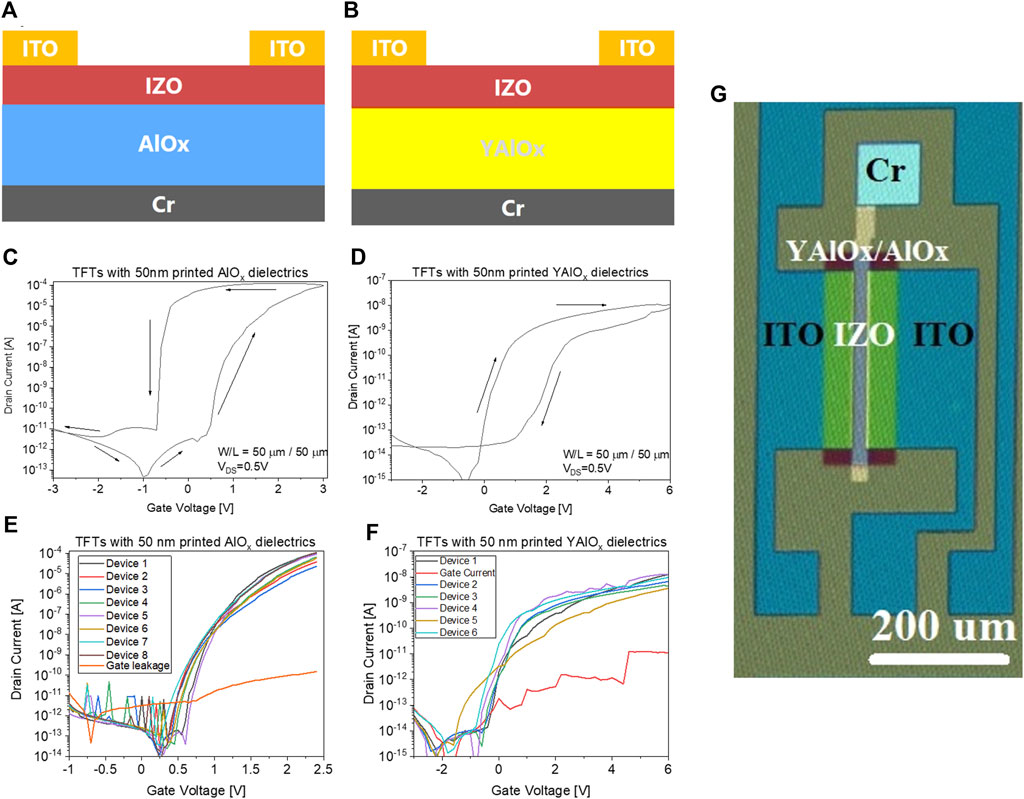
FIGURE 1. (A) Schematic of the TFTs with AlOx only dielectrics. (B) Schematic of the TFTs with YAlOx only dielectrics. (C,D) Full sweep of the gate bias in the transfer characteristics resulting in the opposite direction of hysteresis. (E,F) Transfer characteristics of several TFTs (G) Optical microscope image of a fabricated TFT.
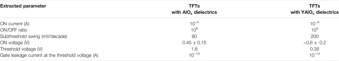
TABLE 1. Device parameters of the TFTs with a single type of dielectric layers.
The devices with AlOx dielectrics have four orders of magnitude higher ON current than their YAlOx employing counterparts. This behavior can be related to the electrolyte behavior of the solution-processed AlOx dielectrics. YAlOx dielectrics have been reported to have minimal to almost no dispersion in their capacitance values at the 0.1 Hz- 1 MHz frequency range (Gillan et al., 2021). The permittivity of YAlOx was extracted as 9.1 in our previous study (Bolat et al., 2019). The permittivity of the printed and low-T (250°C) cured AlOx can be as high as 40 at the quasi-static frequency levels. Still, this would yield only one order of magnitude difference in the ON current by itself. In addition to the electric double-layer capacitance, faradaic charge exchanges at the quasi-static frequency levels (Liang et al., 2020b), reflects as several orders of magnitude increase in the capacitance of the MOS capacitor. This can explain the difference in the ON current of the devices observed here, as well.
The TFTs with AlOx dielectrics suffer from counterclockwise hysteresis (positive charge trapping) in their turn-off transients (Figure 1C). The full sweep of the transfer characteristics of the YAlOx employing devices instead reveals clockwise hysteresis (Figure 1D). Clockwise hysteresis results from negative charge trapping within the dielectric and/or in the dielectric semiconductor interface (Cross and De Souza, 2006). The trapped negative charges screen the effect of the gate bias, and the accumulated channel region depletes at higher voltages than expected during the turn-off transient. A conclusion on these results is that, on the one hand, the gate stacks employing printed AlOx or YAlOx are not suitable by themselves for hysteresis-free switching applications. Observation of the opposite direction of hysteresis (countersign charge trapping), on the other hand, ignites the idea of implementing a bilayer scheme, which can minimize the hysteretic behavior in the switching after the thicknesses are optimized. To prove the hypothesis, TFTs with bilayer AlOx/YAlOx dielectric stack were manufactured via spin coating of the metal-oxide layers and following the fabrication as mentioned in the experimental section for device manufacturing. The total thickness of the dielectric layer stack was reduced to ∼30 nm to provide better gate control and reduce the operating voltage of the devices. Ellipsometry measurements were performed to determine the thickness of the layers. Table 2 shows the extracted refractive index from the dielectric stacks along with the measured thickness. A Cauchy model was used for fitting the data.
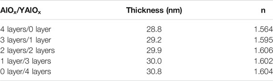
TABLE 2. Thicknesses of the AlOx/YAlOx bilayer dielectrics.
The thicknesses of the layers are in the ∼30
Dielectric stacks with the configurations shown in Table 2 are later implemented in bottom gated TFTs. As the TFTs with AlOx only case and initial experiments with bilayer scheme yielded higher ON currents with AlOx in contact with the channel layer (Figure 1A; Supplementary Figure S1), the AlOx layer was used as the uppermost layer in contact with the semiconducting IZO channel in these experiments, too. Electrical characterizations were performed on the TFTs to investigate the hysteretic behavior. Transfer characteristics of the devices are shown in Figure 2. For an easy understanding, the samples were given the names according to the number of YAlOx layers inside, i.e., 0 layer YAlOx, 1 layer YAlOx, 2 layers YAlOx, and 3 layers YAlOx.
FIGURE 2. Transfer characteristics of the TFTs with bilayer AlOx/YAlOx dielectrics of alternating layer configurations.
Obtained characteristics reveal that the counterclockwise hysteresis is present for the 0 layers YAlOx and 1-layer YAlOx dielectrics cases. Devices with 2 layers of YAlOx dielectrics show minimal hysteresis, whereas the 3 layers YAlOx employing devices have clockwise hysteresis in their transfer characteristics. From these results, one can conclude that by alternating the layer thicknesses in the insulator stack, it is possible to obtain hysteresis-free switching in the bottom gated solution-processed oxide TFTs, even without an encapsulation layer. Table 3 shows the device parameters extracted from the transfer characteristics.
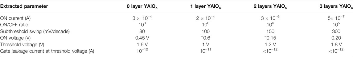
TABLE 3. Device parameters of the TFTs with bilayer dielectric layers.
C-V characteristics were obtained from MOS capacitors with 100 μm × 100 µm areas at various frequencies to understand the device operation better. Figure 2A shows the frequency dispersion of the dielectric constant for the bilayer dielectrics. Figure 2B shows the measurement results at 10 Hz, the lowest measurement frequency, which is later, used to minimize the overestimation in the extracted mobility of the devices.
Electrolyte behavior supported by the low-frequency dispersion of capacitance is diminished with the insertion of 2 layers (∼15 nm YAlOx) dielectric into the insulator stack. Transient current analyses were performed on the MOS capacitors to estimate a time-dependent behavior for the effective charge trapping in the structures. Pulses of 3 V were applied to the gate for two different periods, while the semiconductor contact was kept at ground level. Finally, the resulting transient current was measured at a gate bias of −3 V. Figure 3 shows the obtained results.
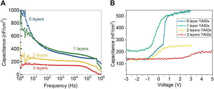
FIGURE 3. (A) Frequency dispersion of the areal capacitance in the bilayer AlOx/YAlOx dielectrics measured at 3 V. (B) C-V characteristics of the MOS capacitors with bilayer AlOx/YAlOx dielectrics and IZO channel layer.
Since long filling times (∼seconds range) are required to observe transients, the measured signals can be assigned to ionic rather than electronic defects, since electronic defects should already be visible at a filling time of 1 ms, but not ionic defects. (Futscher et al., 2020). Residuals in the AlOx dielectrics, such as H+ and OH− ions, were reported partly responsible for the enhanced quasi-static frequency polarization in the dielectric (Daunis et al., 2018; Bolat et al., 2020; Liang et al., 2020b). Secondary ion mass spectroscopy (SIMS) measurements were performed on the bilayer dielectrics spin-coated on Si wafers to investigate the hypothesis in detail. OH− and H+ and C signals were measured across the dielectric stack, and the results are demonstrated in Figure 4.
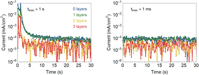
FIGURE 4. Transient current measurements from MOS capacitors with alternating bilayer dielectric thicknesses.
H+ signal level is higher in the 4 layers AlOx and 1 layer YAlOx samples compared to the samples with thicker YAlOx layers. C signal is at the detection noise level in all the layers. A closer look at the H+ and OH− signals from the layers is provided in Figure 5.
FIGURE 5. SIMS profile shows residuals’ behaviors (H+, OH−, and C) across the AlOx/YAlOx layer stacks.
H+ and OH− signals have significantly higher levels for the AlOx and 1 layer YAlOx samples, supporting the positive charge trapping in the dielectric due to ion movement and charge exchange in the vicinity of the gate-dielectric interface. The H+ and OH− signal suppresses at the onset of YAlOx layer in the samples with thicker YAlOx layers (blue and green curves), which can explain the decrease of the dielectric constant at the low-frequency regime. As the OH− and H+ ion movement towards the bottom of the dielectric is blocked, the ionic charge movement and charge exchange between gate and dielectric diminishes, which suppresses the electric double-layer capacitance.
For an ease of understanding, we explain the charge trapping, ion migration and suppression of such migration mechanism in the bilayer dielectrics as follows:
Under the field effect of the gate bias, the water molecules in the AlOx dielectric dissociate into H+ and OH- ions. H+ and OH- ions move towards the semiconductor and gate contacts, respectively. This results in the electric double layer formation at the interfaces as also reported in previous works (Yuan et al., 2010; Daunis et al., 2018; Liang et al., 2020b). Existence of the H+ ions at the oxide semiconductor interface further enhances the field effect by orders of magnitude due to the faradaic charge exchange between the adsorbed H+ ions and semiconductor, resulting in the pseudocapacitance. This process can be considered as protonation of the semiconductor dielectric interface and was also reported by Yuan et al. for a H2O doped electrolyte ZnO interface (Yuan et al., 2010). Since the dehydrogenation requires a large energy, channel stays ON until a large negative bias is applied from the gate contact (Figure 6). For the devices with YAlOx dielectrics, the ion movement blocking takes effect for the scenarios where the YAlOx thickness is more than 10 nm. For the single layer case (1 layer YAlOx), the H+ and OH- ions are not suppressed and can reach until the gate, as confirmed by SIMS measurements (Figure 5). For the bilayer dielectric containing stacks with YAlOx thickness >10 nm, use of AlOx at the insulator semiconductor interface results in a higher ON current than the devices where YAlOx is placed in contact with the semiconducting channel layer, despite using identical thicknesses for each material. This can be seen in Supplementary Figure S1 and be related to the hydrogen rich nature of the AlOx resulting in the electron donation to the channel, as reported by Daunis et al. and also by Zermault and Subramanian. (Zeumault and Subramanian, 2016; Daunis et al., 2018).
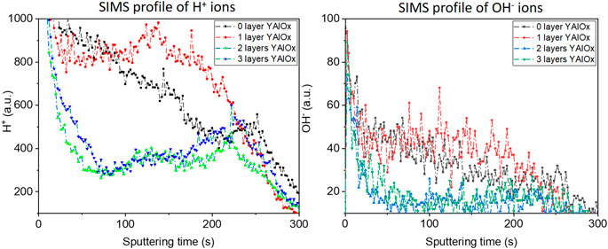
FIGURE 6. Comparison of SIMS profiles of H+ and OH− through the depth of the bilayer dielectrics.
Devices with two layers YAlOx dielectrics were characterized electrically to obtain their output characteristics since the minimal hysteresis was obtained for this dielectric configuration. Results are shown in Figure 7. µFE is extracted from the output characteristics at a drain voltage of 3 V in the saturation region using Eq. 1 as ∼1.5 cm2/V.sec.
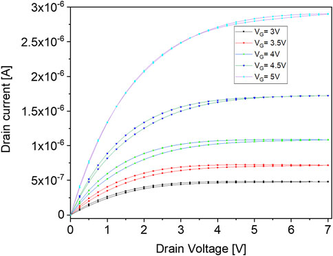
FIGURE 7. Output characteristics of the TFTs with 2 layers YAlOx dielectrics.
It is important to consider that the mobility is not affected only by the dielectric itself, the low temperature processing also results in high amount of hydroxides in the semiconducting layers, thereby reducing the mobility of the devices. Daunis et al. also reported reduction of the extracted mobility with the insertion of ion blocking dielectric layer into the gate stack, where they observed a reduction from 117 cm2/V.sec to 4.6 cm2/V.sec after the suppression of the hysteretic behavior (Daunis et al., 2018).
Solution processing promises low-cost manufacturing of oxide electronics on flexible substrates. This requires temperature reduction of the post deposition annealing of the as-deposited precursors, which results in anomalous charge trapping in the dielectric layers. In this work, the effects of implementing two counterbalancing charge-trapping dielectrics (YAlOx and AlOx) in low-temperature cured solution-processed TFTs were investigated. Increasing the thickness of the negative charge trapping YAlOx in the bilayer dielectric stack was observed to diminish the EDL capacitance thought to be originated from H+ and OH− ion migration in the AlOx dielectrics. Detailed SIMS analysis revealed the significant decrease of the H+ and OH− ions in the YAlOx dielectrics, supporting the hypothesis. A stack of 15 nm YAlOx 15 nm AlOx offered hysteresis-free transistor switching, providing an alternative methodology to obtain stable operation. This methodology can be extended to various insulators with counterbalancing charge trapping and provide a general manufacturing route for high-performance, stable switching low-temperature solution-processed oxide transistors.
Ink preparation: YAlOx (Y: Al, 2:8) and AlOx inks were prepared by dissolving Al(NO3)3 × 9H2O and Y(NO3)3 × 6H2O salts in 50%/50% volume 2-Methoxyethanol/Ethylene glycol. Nominal metal ion concentration was adjusted as 0.4 M for printed dielectrics and 0.1 M for spin-coated layers. Solutions were stirred at 70°C for 12 h and filtered with a 0.2 µm PFTE filter. The viscosity of the printing ink was measured at 25°C by a strain-controlled rheometer (Anton-Paar MCR 301) with plate/plate geometry (25 mm diameter, 0.1 mm gap). It was obtained as 12 cP falling in a suitable range for inkjet printing.
IZO ink was prepared by dissolving In(NO3)3. xH2O and Zn(NO3)2 × 6H2O with a total metal ion concentration of 0.2 M (In: Zn, 7:3) in 2-Methoxyethanol. The nominal metal ratio was chosen according to the reported literature (Mancinelli et al., 2020). The solution was stirred at 60°C for 12 h and filtered with a 0.2 µm PFTE filter before deposition.
TFT fabrication: A test-grade silicon wafer serving as the substrate was sonicated in acetone (5 min), isopropanol (5 min), and DI water (5 min). Cleaned substrates underwent a buffered oxide etchant exposure to remove the native oxide from the wafers. 100 nm thick SiNx was deposited via plasma-enhanced chemical vapor deposition at 150°C to isolate the devices from the substrate. E-beam evaporated Cr (35 nm) was used as gate contact and patterned via photolithography. Dielectric layers were deposited as follows:
Printed AlOx and YAlOx dielectrics: AlOx and YAlOx were inkjet printed with a resolution of 400 drops-per-inch via LP50 inkjet printer with Dimatix cartridges of 10 pL nozzle volume. Two layers of dielectric ink were printed to avoid pinholes in the insulator. Printed layers were dried at 250°C, and were exposed to DUV with N2 flow (6 L/min) for 30 min. DUV annealing is performed with a low-pressure mercury lamp (Filgen Inc. UV253H) with two emission peaks at 184 and 253 nm and output power density of 25–28 mW/cm2. Final annealing at 250°C (60 min) in air ambient was applied to densify the cured layers further.
Spin-coated AlOx and YAlOx dielectrics: 4 layers of dielectrics layers were created by spin-coating at a speed of 4,000 rpm and subsequent drying at 150°C for 5 min. Before every spin-coating, the substrates were exposed to 1 min of oxygen plasma to enhance the wetting of the subsequent layers. Dried layers were exposed to DUV with N2 flow (6 L/min) for 30 min and later annealed in air at 250°C for 30 min.
Spin-coated IZO channel layer: Two consecutive layers of IZO ink were spin-coated with a speed of 2000 rpm for 30 s and dried at 150°C. The dried semiconductor layer underwent the DUV exposure in the air for 30 min and the last annealing step at 250°C for 60 min 30 nm thick semiconductor channel was photolithographically patterned and etched with a 1:121 diluted hydrochloric acid solution.
Sputtered ITO contacts: Source and drain contacts were realized via sputtering and lift-off of ITO layers with the following parameters: Sputtering pressure: 0.4 Pa, O2 Flow:0 sccm, Ar Flow: 60 sccm, RF sputtering power: 180 W, deposition temperature: room temperature, the thickness of the layer ∼100 nm. The sheet resistance of the layer was ∼25 ohms/square.
Electrical characterizations: DC characteristics of the TFTs were acquired in the dark with a Keithley 4,200 Semiconductor parameter analyzer. C-V, C-f, and transient measurements on MOS capacitors were performed by using Paios from Fluxim AG. C-V and C-f measurements were performed using an AC voltage of 50 mV.
SIMS measurements: The primary beam was 25 keV Bi+ ions with a total current of 1.1 pA and a raster size of 50 × 50 μm2. For detection of negative ions, Cs+ ions were used with 500 eV ion energy, 30 nA pulse current on a 300 × 300 μm2 raster size to bombard and etch the film.
Optical characterizations: Optical characterization and thickness measurement of the AlOx/YAlOx bilayer dielectrics deposited on Si(<100>) was acquired by ellipsometry (J.A. Woollam M-2000V). The bilayer was modelled as a Bruggeman effective medium approximation (EMA) layer. The fitting was performed using the CompleteEASE software by J.A. Woollam Co.
The original contributions presented in the study are included in the article/Supplementary Material, further inquiries can be directed to the corresponding authors.
SB and YR conceptualized the idea. SB fabricated the devices. EA performed the electrical characterizations on the TFTs with bilayer AlOx/YAlOx dielectrics, critically analyzed the obtained results, and discussed them with SB, YR, EA, SB, and MF performed the C-f, C-V, and transient current measurements on the MOS capacitors. IS supervised the electrical characterizations. S-CY optimized the sputtering recipe for the ITO contacts and performed the SIMS characterization and analysis on the bilayer dielectrics. AA performed ellipsometry measurements and fitted the obtained results for thickness and optical constant extractions of the layers. YR supervised the study. SB and YR wrote the manuscript with the inputs from all the coauthors. SB and EA contributed equally to this work.
MHF is supported by a Rubicon Fellowship from the Netherlands Organisation for Scientific Research (NWO).
The authors declare that the research was conducted in the absence of any commercial or financial relationships that could be construed as a potential conflict of interest.
All claims expressed in this article are solely those of the authors and do not necessarily represent those of their affiliated organizations, or those of the publisher, the editors and the reviewers. Any product that may be evaluated in this article, or claim that may be made by its manufacturer, is not guaranteed or endorsed by the publisher.
Authors acknowledge the financial support from the Strategic Focus Area Advanced Manufacturing of the ETH domain under the project FOXIP - Functional OXIdes Printed on Polymers and Paper.
The Supplementary Material for this article can be found online at: https://www.frontiersin.org/articles/10.3389/felec.2021.804474/full#supplementary-material
Barquinha, P., Martins, R., Pereira, L., and Fortunato, E. (2012). Transparent Oxide Electronics. Chichester, UK: John Wiley & Sons. doi:10.1002/9781119966999
Bolat, S., Fuchs, P., Knobelspies, S., Temel, O., Sevilla, G. T., Gilshtein, E., et al. (2019). Inkjet‐Printed and Deep‐UV‐Annealed YAlO X Dielectrics for High‐Performance IGZO Thin‐Film Transistors on Flexible Substrates. Adv. Electron. Mater. 5, 1800843. doi:10.1002/aelm.201800843
Bolat, S., Torres Sevilla, G., Mancinelli, A., Gilshtein, E., Sastre, J., Cabas Vidani, A., et al. (2020). Synaptic Transistors with Aluminum Oxide Dielectrics Enabling Full Audio Frequency Range Signal Processing. Sci. Rep. 10, 16664. doi:10.1038/s41598-020-73705-w
Cheong, H., Ogura, S., Ushijima, H., Yoshida, M., Fukuda, N., and Uemura, S. (2015). Rapid Preparation of Solution-Processed InGaZnO Thin Films by Microwave Annealing and Photoirradiation. AIP Adv. 5, 067127. doi:10.1063/1.4922512
Cross, R. B. M., and De Souza, M. M. (2006). Investigating the Stability of Zinc Oxide Thin Film Transistors. Appl. Phys. Lett. 89, 263513. doi:10.1063/1.2425020
Daunis, T. B., Tran, J. M. H., and Hsu, J. W. P. (2018). Effects of Environmental Water Absorption by Solution-Deposited Al2O3 Gate Dielectrics on Thin Film Transistor Performance and Mobility. ACS Appl. Mater. Inter. 10, 39435–39440. doi:10.1021/acsami.8b15592
Fortunato, E., Barquinha, P., and Martins, R. (2012). Oxide Semiconductor Thin-Film Transistors: A Review of Recent Advances. Adv. Mater. 24, 2945–2986. doi:10.1002/adma.201103228
Futscher, M. H., Gangishetty, M. K., Congreve, D. N., and Ehrler, B. (2020). Quantifying mobile Ions and Electronic Defects in Perovskite-Based Devices with Temperature-dependent Capacitance Measurements: Frequency vs Time Domain. J. Chem. Phys. 152, 044202. doi:10.1063/1.5132754
Gillan, L., Li, S., Lahtinen, J., Chang, C. H., Alastalo, A., and Leppäniemi, J. (2021). Inkjet‐Printed Ternary Oxide Dielectric and Doped Interface Layer for Metal‐Oxide Thin‐Film Transistors with Low Voltage Operation. Adv. Mater. Inter. 8, 2100728. doi:10.1002/admi.202100728
Gilshtein, E., Bolat, S., Sevilla, G. T., Cabas‐Vidani, A., Clemens, F., Graule, T., et al. (2020). Inkjet‐Printed Conductive ITO Patterns for Transparent Security Systems. Adv. Mater. Technol., 2000369. doi:10.1002/admt.202000369
Hwang, M.-s., Jeong, B.-y., Moon, J., Chun, S.-K., and Kim, J. (2011). Inkjet-printing of Indium Tin Oxide (ITO) Films for Transparent Conducting Electrodes. Mater. Sci. Eng. B 176, 1128–1131. doi:10.1016/j.mseb.2011.05.053
Jin, J. W., Nathan, A., Barquinha, P., Pereira, L., Fortunato, E., Martins, R., et al. (2016). Interpreting Anomalies Observed in Oxide Semiconductor TFTs under Negative and Positive Bias Stress. AIP Adv. 6, 085321. doi:10.1063/1.4962151
Kim, M.-G., Kanatzidis, M. G., Facchetti, A., and Marks, T. J. (2011). Low-temperature Fabrication of High-Performance Metal Oxide Thin-Film Electronics via Combustion Processing. Nat. Mater 10, 382–388. doi:10.1038/nmat3011
Kim, S. J., Yoon, S., and Kim, H. J. (2014). Review of Solution-Processed Oxide Thin-Film Transistors. Jpn. J. Appl. Phys. 53, 02BA02. doi:10.7567/JJAP.53.02BA02
Kim, Y.-H., Heo, J.-S., Kim, T.-H., Park, S., Yoon, M.-H., Kim, J., et al. (2012). Flexible Metal-Oxide Devices Made by Room-Temperature Photochemical Activation of Sol-Gel Films. Nature 489, 128–132. doi:10.1038/nature11434
Kim, Y. G., Lv, D., Huang, J., Bukke, R. N., Chen, H., and Jang, J. (2020). Artificial Indium‐Tin‐Oxide Synaptic Transistor by Inkjet Printing Using Solution‐Processed ZrO X Gate Dielectric. Phys. Status Solidi A. 217, 2000314. doi:10.1002/pssa.202000314
Knobelspies, S., Bierer, B., Daus, A., Takabayashi, A., Salvatore, G., Cantarella, G., et al. (2018). Photo-Induced Room-Temperature Gas Sensing with A-IGZO Based Thin-Film Transistors Fabricated on Flexible Plastic Foil. Sensors 18, 358. doi:10.3390/s18020358
Lee, E., Ko, J., Lim, K.-H., Kim, K., Park, S. Y., Myoung, J. M., et al. (2014). Gate Capacitance-dependent Field-Effect Mobility in Solution-Processed Oxide Semiconductor Thin-Film Transistors. Adv. Funct. Mater. 24, 4689–4697. doi:10.1002/adfm.201400588
Lee, J., Seul, H., and Jeong, J. K. (2018). Solution-processed Ternary alloy Aluminum Yttrium Oxide Dielectric for High Performance Indium Zinc Oxide Thin-Film Transistors. J. Alloys Compounds 741, 1021–1029. doi:10.1016/j.jallcom.2018.01.249
Liang, X., Li, Z., Liu, L., Chen, S., Wang, X., and Pei, Y. (2020a). Artificial Synaptic Transistor with Solution Processed InOx Channel and AlOx Solid Electrolyte Gate. Appl. Phys. Lett. 116, 012102. doi:10.1063/1.5120069
Liang, X., Liu, L., Cai, G., Yang, P., Pei, Y., and Liu, C. (2020b). Evidence for Pseudocapacitance and Faradaic Charge Transfer in High-Mobility Thin-Film Transistors with Solution-Processed Oxide Dielectrics. J. Phys. Chem. Lett. 11, 2765–2771. doi:10.1021/acs.jpclett.0c00583
Liu, A., Zhu, H., Guo, Z., Meng, Y., Liu, G., Fortunato, E., et al. (2017). Solution Combustion Synthesis: Low-Temperature Processing for P-type Cu:NiO Thin Films for Transparent Electronics. Adv. Mater. 29, 1701599. doi:10.1002/adma.201701599
Mancinelli, A., Bolat, S., Kim, J., Romanyuk, Y. E., and Briand, D. (2020). Deep-UV-Enhanced Approach for Low-Temperature Solution Processing of IZO Transistors with High-K AlOx/YAlOx Dielectric. ACS Appl. Electron. Mater. 2, 3141–3151. doi:10.1021/acsaelm.0c00444
Paterson, A. F., and Anthopoulos, T. D. (2018). Enabling Thin-Film Transistor Technologies and the Device Metrics that Matter. Nat. Commun. 9, 5264. doi:10.1038/s41467-018-07424-2
Petti, L., Münzenrieder, N., Vogt, C., Faber, H., Büthe, L., Cantarella, G., et al. (2016). Metal Oxide Semiconductor Thin-Film Transistors for Flexible Electronics. Appl. Phys. Rev. 3, 021303. doi:10.1063/1.4953034
Smith, J. T., Shah, S. S., Goryll, M., Stowell, J. R., and Allee, D. R. (2014). Flexible ISFET Biosensor Using IGZO Metal Oxide TFTs and an ITO Sensing Layer. IEEE Sensors J. 14, 937–938. doi:10.1109/JSEN.2013.2295057
Wager, J. F. (20201975). TFT Technology: Advancements and Opportunities for Improvement. Inf. Display 36, 9–13. doi:10.1002/msid.1098
Wang, B., Huang, W., Chi, L., Al-Hashimi, M., Marks, T. J., and Facchetti, A. (2018). High-k Gate Dielectrics for Emerging Flexible and Stretchable Electronics. Chem. Rev. 118, 5690–5754. doi:10.1021/acs.chemrev.8b00045
Yuan, H., Shimotani, H., Tsukazaki, A., Ohtomo, A., Kawasaki, M., and Iwasa, Y. (2010). Hydrogenation-Induced Surface Polarity Recognition and Proton Memory Behavior at Protic-Ionic-Liquid/Oxide Electric-Double-Layer Interfaces. J. Am. Chem. Soc. 132, 6672–6678. doi:10.1021/ja909110s
Zeumault, A., and Subramanian, V. (2016). Mobility Enhancement in Solution-Processed Transparent Conductive Oxide TFTs Due to Electron Donation from Traps in High-kGate Dielectrics. Adv. Funct. Mater. 26, 955–963. doi:10.1002/adfm.201503940
Keywords: solution processing, metal oxides, dielectrics, low temperature curing, charge trapping, thin-film transistor (TFT)
Citation: Bolat S, Agiannis E, Yang S-C, Futscher MH, Aribia A, Shorubalko I and Romanyuk YE (2022) Engineering Bilayer AlOx /YAlOx Dielectric Stacks for Hysteresis-Free Switching in Solution-Processed Metal-Oxide Thin-Film Transistors. Front. Electron. 2:804474. doi: 10.3389/felec.2021.804474
Received: 29 October 2021; Accepted: 06 December 2021;
Published: 07 January 2022.
Edited by:
Giovanni Antonio Salvatore, Ca’ Foscari University of Venice, ItalyReviewed by:
Fei Hui, Technion Israel Institute of Technology, IsraelCopyright © 2022 Bolat, Agiannis, Yang, Futscher, Aribia, Shorubalko and Romanyuk. This is an open-access article distributed under the terms of the Creative Commons Attribution License (CC BY). The use, distribution or reproduction in other forums is permitted, provided the original author(s) and the copyright owner(s) are credited and that the original publication in this journal is cited, in accordance with accepted academic practice. No use, distribution or reproduction is permitted which does not comply with these terms.
*Correspondence: Sami Bolat, c2FtaS5ib2xhdEBlbXBhLmNo; Yaroslav E. Romanyuk, WWFyb3NsYXYucm9tYW55dWtAZW1wYS5jaA==
†These authors have contributed equally to this work
Disclaimer: All claims expressed in this article are solely those of the authors and do not necessarily represent those of their affiliated organizations, or those of the publisher, the editors and the reviewers. Any product that may be evaluated in this article or claim that may be made by its manufacturer is not guaranteed or endorsed by the publisher.
Research integrity at Frontiers
Learn more about the work of our research integrity team to safeguard the quality of each article we publish.