 Yassine Madoune
 DingBang Yang1†
 Yameen Ahmed
- 1Hunan Key Laboratory of Super-microstructure and Ultrafast Process, School of Physics and Electronics, Central South University, Changsha, China
- 2Department of Electrical and Computer Engineering, University of Victoria, Victoria, BC, Canada
Atomically thin layered transition metal dichalcogenides (TMDs), such as MoS2 and WS2, have been getting much attention recently due to their interesting electronic and optoelectronic properties. Especially, spiral TMDs provide a variety of candidates for examining the light-matter interaction resulting from the broken inversion symmetry, as well as the potential new utilization in functional optoelectronic, electromagnetic and nanoelectronics devices. To realize their potential device applications, it is desirable to achieve controlled growth of these layered nanomaterials with a tunable stacking. Here, we demonstrate the Physical Vapor Deposition (PVD) growth of spiral pyramid-shaped WS2 with ∼200
Introduction
Two-dimensional (2D) layered transition metal dichalcogenides (TMDs) have emerged as promising candidates for optoelectronic devices due to a plentiful choice of materials (Mak et al., 2010) (Xiao et al., 2022) (Yang et al., 2017). Multilayer TMDs display unique optoelectronic properties dependent on the layer number, such as a transition from the indirect band gap in multilayer to the direct band gap in monolayer (Manzeli et al., 2017). The different stacking modes also have critical effects on the properties of TMDs (Fan et al., 2017; Sarma et al., 2019) (Ci et al., 2022). It appeared that polarization enhancement with two petals along staggered stacking direction in 3R MoS2 (Shi et al., 2017). The 3R-like TMDs few layers and spiral structures also show high degree of SHG polarization at room temperature due to the inversion symmetry breaking (Ma et al., 2021). Furthermore, bilayer or multilayer TMDs materials with different twisted angles always exhibit a different interlayer coupling to tune the properties of TMDs (Wang et al., 2019).
Spiral TMDs structures display more complex stacking than 2H stacking multilayer structures such as continuously supertwisted stacking, richer physical, and chemical effects (Ci et al., 2022) (Tong et al., 2022). Screw dislocation is a typical line defect for the materials and the growth driven by spiral dislocation is a classic crystal growth mode at relatively low supersaturation (Cain et al., 2016) (Forticaux et al., 2015) (Meng et al., 2013). Many methods have been developed for the fabrication of spiral TMDs, including chemical vapor deposition (CVD) and physical vapor deposition (PVD) (Barman et al., 2019) (Wang et al., 2019) (Hao et al., 2016) (Fan et al., 2018). The hybrid spiral-like MoS2 crystals with distinctive electrostatic properties have been synthesized through increasing the growth temperature to 1,000°C by CVD method (Hao et al., 2016). The spiral WS2 with non-linear optical effects, a high value of valley polarization could be prepared by CVD using a mixture of WO3, and S as precursors (Barman et al., 2019) (Fan et al., 2017). Compared with CVD method, PVD method is simpler, pollution-free as well as can synthesize spiral TMDs which have higher hardness, better thermal stability, and more stable chemical properties. The controllable growth of layer by layer and spiral WS2 with ∼30
Here, we report a controllable growth of large size (∼200
Materials and methods
To synthesize WS2 nanoflakes, a ceramic boat filled with WS2 (ALDRICH, 99%) powder (0.4 g) was placed at the heating center of a 2-inch quartz tube (2-inch diameter, 60 cm length), a three-piece of SiO2/Si (300 nm, 1.5
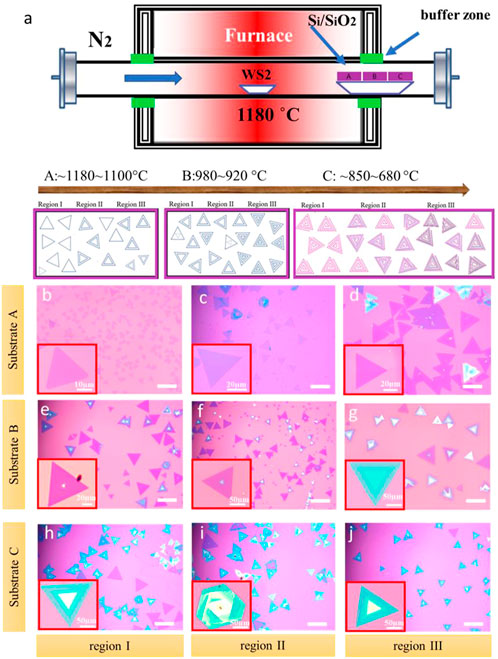
FIGURE 1. Controllable growth and Optical image of the Layer-By-Layer Structures and Spiral Structures of WS2 (A) Schematic Illustration of the PVD experiment setup for TMD synthesis. The distribution of WS2 from the substrate of (A–C): Monolayers, Bilayers. A few layers, Layer-By-Layer (LBL) and spiral structures. (B–D) The optical images of Ⅰ (monolayer), Ⅱ (a mixture of bilayers and trilayer) and Ⅲ (few layers) regions on substrate (A) (E–G) The optical images of Ⅰ and Ⅱ (multilayers) and Ⅲ (layer by layer) regions on substrate (B) (H–J) The optical images of Ⅰ (single-spiral pattern), Ⅱ (double-spiral patterns) and Ⅲ (multi-spiral patterns) regions on substrate (C).
Results and discussion
We design a PVD method to prepare monolayer (ML), few layers (FL), layer by layer (LBL), and spiral WS2, as shown in Figure 1A. The distances between substrates A, B, and C and WS2 powder (heating center) are 6 cm, 8 cm, and 10 cm, respectively, where the growth temperature can be controlled well. The growth temperature of substrate A was 1,180°C which was inside the tube, that of substrate C was ∼680°C–850°C which was at the end of the estuary, nearly outside the oven chamber, and that of substrate B was ∼920°C–980°C which was in the middle of the estuary. Figures 1B–D show that many monolayers and a few layers WS2 were synthesized on substrate A with a high temperature ranging from 1,100°C to 1,180°C. The region Ⅰ of substrate A displays the monolayer WS2 with regular triangle and an average size of 30 μm–40 μm as shown in lower-left corner of Figure 1B. The region Ⅱ of substrate A contains a mixture of bi/trilayer WS2 with an average size of about 50 μm–60 μm (Figure 1C). The region Ⅲ of substrate A, as shown in Figure 1D, contains multilayers with an average size of about 70 μm–90 μm where the temperature in this area reaches approximately 1,100°C, lower than the Ⅰ region of substrate A. Multilayers and LBL structures are synthesized on substrate B with a temperature ranging from 920°C to 980°C, as shown in Figures 1E–G. For substrate B, the number of layers increases from multilayers in region I to AA or AB stacking in region Ⅱ with an increase in size from 90 μm to 100 μm to 120 μm–150 μm. The LBL structures are synthesized in the region Ⅲ on substrate B with an estimated size of 180 μm–220 μm, which suggests a flat triangular top on a larger and thinner flake. As the temperature decreasing further, the spiral patterns of WS2 were observed on substrate C. The structures in region I (Figure 1H) present a single spiral pattern with an average size of ∼220 μm where the temperature is approximately 850°C. Compared to region I, region Ⅱ (Figure 1I) has double spiral patterns with temperatures between 850°C and 680°C. The region Ⅲ (Figure 1J) exhibits more intricate multi-spiral patterns with a temperature near 680°C. The average size of double spiral and multi-spiral patterns is ∼200 μm. Compared with LBL growth above, the size of WS2 obtained by spiral growth did not have an obvious difference with the decreasing temperature.
We found that a monolayer is formed at a high temperature with small sizes, that the sizes, the number of layers increase little by little as the temperature decreases to form a LBL, and SDD structures in the end (Morin et al., 2011). With the temperature decreasing, the LBL and the size of spiral WS2 reaches ∼220 µm with a total area over 0.3 cm2
The PVD-deposited 2H-WS2 nanoplates have a variety of morphologies, including triangles, truncated triangles, hexagons, etc (Figures 1B–J). The surface free energy of the relevant crystal face affects the development rate of the crystal face in 2D crystals, where the surface free energy corresponds to the crystal’s edge free energy. When the free energy is high, the crystal edge is exceedingly unstable. At this point, the free electrons in the free state will be swiftly absorbed to form the edge in a stable state of low free energy, causing the edge of high free energy to develop fast and the edge of low free energy to grow slowly (Park et al., 2017; Wang et al., 2018). As a consequence of the fast growth behavior, the crystal face with high free energy will ultimately get smaller or vanish. On the contrary, the slow-growing crystal face will eventually become the biggest (Li et al., 2018). As a result, the final crystal form will be connected to the development rate of various kinds of edge terminals, which is further influenced by the precursor volume ratio, which directly influences the growth rate of distinct crystal planes. We employed a constant flow in a quartz tube to retain the precursor to establish a stable air flow environment, which guarantees that the WS2 vapor is thoroughly volatilized and evenly dispersed throughout the reaction process. As a result, the concentration distribution of WS2 precursors (volatilization and diffusion) may be regarded as the primary factor influencing the various form morphologies (Yan et al., 2023).
Figure 2A shows the illustrations of LBL WS2 structures. There are many possible WS2 stacking configurations but two of the most important are the AB-stacking and the AA-stacking configurations, as shown in Supplementary Figure S2B (Rudenko et al., 2021). Figure 2B shows the SEM images of high-coverage LBL structures in substrate B of region III with a size of 200 μm. Figure 2C shows that the AFM image corresponds to the marked red square in Figure 2B, which confirms the LBL growth of WS2. The line profile in Figure 2C indicates that the height increases gradually from edge to center and the height of each step is ∼0.72 nm, consistent with monolayer WS2. Figure 2D shows the Raman intensity mapping of
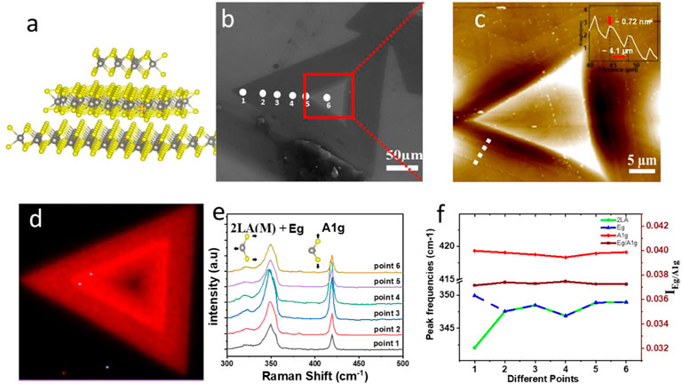
FIGURE 2. Layer by Layer (LBL) growth. (A) Illustrations of the crystal LBL structure. (B) SEM image of WS2 LBL structure. (C) AFM image corresponding to the marked red square in SEM image. (D) Raman intensity mapping of
Figure 2F shows that both
The anisotropic pyramidal growth is continued in this fashion (formed) by self-perpetuating steps of SDD layers. Under mild supersaturation circumstances, screw dislocations form step edges (slipped planes) in the bottom layer (Daher et al., 2018). Because of the large concentration of precursors, the unintentional rising of a grain boundary caused by varying growth rates of multiple edge terminations begins spiral growth, which is schematically shown as step 1 in Figure 3A. The spiral development is also catalyzed by the uneven surface of the substrate, which is created by the partial etching of SiO2/Si using piranha and plasma treatment. The unsaturated sulfur edges in the slipping plane operate as nucleation sites for additional precursor atom addition, resulting in the formation of the second layer on top of the bottom layer, as illustrated in Figure 3A (steps 2, 3). The growth process continues up to an interface or a nodal point, generating a spiral after the slip plane is produced with vertically mismatched edges (Sarma et al., 2019).
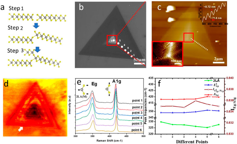
FIGURE 3. Screw dislocation growth of single spiral. (A) Illustrations of the single spiral structure (B) SEM image of single spiral structure of WS2 (C) AFM images corresponding the marked areas in SEM image. (D) Raman intensity mapping of
Figure 3B shows a typical SEM image of a single spiral WS2 with ∼220 μm, which indicates the atomically flat surface of WS2. The zoom-in AFM image of the red square region of the SEM image is shown in Figure 3C, revealing that each step height of a single spiral of WS2 is ∼0.72 nm, consistent with the height of monolayer WS2, with an estimated height of ∼25 nm (from the edge to the center). When the single spiral WS2 is projected onto the 2D basal plane, the layer size progressively decreases from the center to the edge, as shown in Supplementary Figure S4. The low-left corner of Figure 3C; Supplementary Figure S5A as well as Supplementary Figure S5B display AFM images of a single spiral, double spiral, and multi-spiral with clear screw dislocation, respectively. The white lines in Supplementary Figure S5 (near the dislocation center) of the core serve as an example of the included angle, defined as the angle between the traces of the many dislocation spirals that share a common core. There may be two sets of included angles between screw dislocation spirals based on the three-fold symmetry of the monolayer TMD structure. The center structure of spiral nanoplates stays as triangular spiral traces whether the included angles are just (0°C, 360°C) or (120°C, 240°C), as shown in low-left corner of Figure 3C; Supplementary Figure S5. In contrast, the center of those spiral nanoplates shows hexagonal spiral traces when we inspect the second set of included angles of (60°C, 180°C, and 300°C) (Shearer et al., 2017). It should be noted that multi-spiral pattern nanostructures are far less often seen compared to single or double-spiral pattern structures.
Figure 3D shows the Raman intensity (350 cm−1) mapping of the spiral structure, revealing a regular variety of
To determine the frequency dependence of the main WS2 Raman peaks (
Figure 4A shows the Optical images of WS2 bilayers with varying twist angles of 2°C,10°C, 12°C, 20°C, 31°C, and 49°C. As a result of the steric repulsion effect, the interlayer coupling in the randomly twisted bilayer was lower than in LBL stacking (AA stacking) (Zhang et al., 2020). Spin-orbit coupling would find a wider range of uses in angle-dependent moiré excitons, spintronics, and valley electronics if the twist angles were varied. It is depicted by the atomic structure schematic of LBL, single spiral patterns hetero-bilayer WS2 in a 2
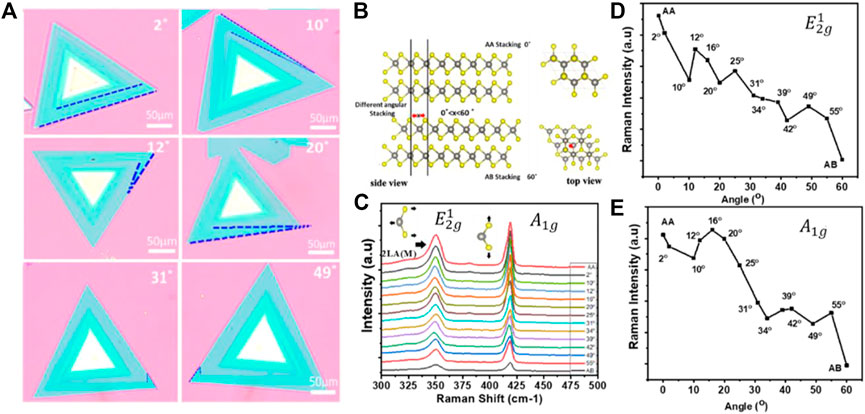
FIGURE 4. Twist angle-dependent responses bilayer WS2 crystals with different twist angles. (A) Optical images and (B) atomic structure of different angles hetero-bilayer stacking WS2 in a 2 × 2 × 1 supercell from a side view (upper panel) and top view (lower panel), respectively. (C) Raman intensity at different twist angles on single spiral bilayer WS2. (D,E) Twist angular dependence of Raman intensity (
Interlayer coupling interactions of SDD (single spiral) differ in randomly twisted bilayers compared to LBL due to the upper and lower layers of multi-spiral pattern nanostructures being far less often seen compared to single or double-spiral pattern structure saving different arrangements of atoms. The majority of 2H-WS2 nanosheets with terraced or spiral structures are dispersed across the substrate, according to the morphological information of 2H-WS2 nanosheets. So, the moiré superlattice from SDD stacking with different twist angles can change the electronic structure of 2D materials, giving them unusual transport properties like unusual superconductivity and insulating behavior. The interlayer exciton coupling can also be controlled, which makes it possible to study moiré excitons, spintronics, and valley electronics of spin-orbit coupling (Jin et al., 2019) (Seyler et al., 2019)
The optical images in Figures 5A, B show the onset of the formation of the single helical pattern, and the LBL, respectively. It is termed anisotropic growth as it is considered the defining feature of growth almost without exception in which cells grow faster in one direction than the other, which describes the condition when the rates of growth are uneven in all directions (Figure 5A). In contrast, when growth rates are the same in all directions, growth is isotropic (LBL in Figure 5B). Figure 5C shows the model diagram of terraced structure growth. The active adsorption atoms are shown by white arrows, and the dislocation core (vc) depicts the axial growth rate, which is governed by the nucleation rate of new atomic layers. Outer edges (vo) denote the lateral growth rate, as determined by the rate at which adsorbed atoms cling to the step’s edge (Yin et al., 2015). The new surface layer progressively emerges throughout the growing phase of a terraced construction as the new atomic layer slowly nucleates on the top surface. Instead of a 1D structure growth, 2D flakes do so because the growth rate of normal to the surface (Rm) is much slower than lateral step velocities (vs). When this situation occurs repeatedly, layered terraced structures will grow layer by layer. It has been discovered that the number of terraced nanosheets would directly depend on the disparity between axial and lateral development speeds. Furthermore, we translate the number of terraced into the vc/vo ratio, which represents the ratio of axial and lateral growth rates. Furthermore, the nucleation rate of new layers on the existing top layer determines the axial growth rate. Only when the current top terraced reaches the critical size, the nucleation of the new atomic layer occurs. Therefore, the axial growth rate can be expressed as (Tersoff et al., 1994): vc = hRcvo, where h is the height of the freshly formed terraced and Rc is the crucial height of the top terraced at the time. According to the variations in supersaturation in the furnace, the ratios of vc/vo and supersaturation have a linear relationship, meaning that the ratio of vc/vo rises as supersaturation rises, which also predicts an increase in the number of terraced fields (Figure 5D). The concentration of adsorption atoms may build up, but the energy barrier at the step’s edge prevents this from happening; therefore, the nucleation of new atoms must overcome this high energy barrier (Krishnamurthy et al., 1993).Therefore, High supersaturation is crucial during the growth process of terraced structures in order to encourage the nucleation of new atomic layers and provide LBL the ability to grow at a favorable crystal growth rate. When the substrate is heated to a high temperature, spiral structures make up the majority of the nanosheets. According to Figure 1A, the nanosheets display a straightforward triangular spiral pattern, which indicates that in contrast to the low-temperature region, the screw dislocation is formed by first forming a step edge at the bottom of the growth process as the nucleation position of a new layer. Then, by continuously adsorbing the precursor atoms, results in the growth of a second layer at the top of the bottom layer, which is faster than that of the first layer.
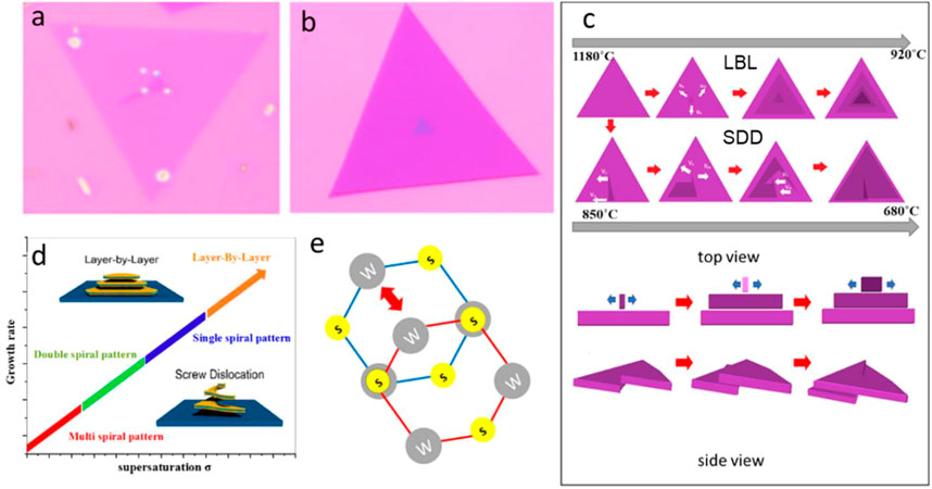
FIGURE 5. Mechanisms Formation of Layer by Layer and Dislocated WS2 Spirals (A,B) Optical image of single spiral pattern and layer by layer WS2, respectively. (C) Schematic diagrams of Layer-By-Layer and screw dislocation propagation process. (D) Schematic illustrations of the growth rate of different dominant crystal growth modes as a function of supersaturation. (E) The tungsten atom in the top layer (red hexagon) positioned at the center of the bottom layer hexagon (blue).
Furthermore, the spiral structures were developed using the SDD growth mode, forming pyramid-shaped WS2 flakes. The Burton-Cabrera-Frank (BCF) crystal growth hypothesis provides an explanation for a number of these pyramidal growths that have been observed in 1D and 2D nanomaterials (Burton et al., 1951) (Fan et al., 2017), which states that the supersaturation of the local growth environment controls the crystal growth process. The degree of supersaturation is denoted as σ = In(c/c0), where c represents the local precursor concentration and c0 represents the equilibrium precursor concentration. The furnace’s temperature profile has an impact on both c and c0. Particularly, the deposition reaction’s thermodynamic equilibrium constant is largely governed by the local temperature, determining the value of c0. The precursor’s heating temperature and the precursor’s movement all dynamically affect the value of c. The deposition temperature largely affects the local supersaturation, which also affects the growth rate of nanostructures. In this theory, the system’s supersaturation drives various growth modes, including LBL and SDD growth (Woodruff, 2015). The nucleation will never be homogenous if the deposition is done on different substrates. There will always be certain defect sites that have a larger chemical potential than the rest of the substrate, which are more active for crystal development. The SDD growth mode is the most advantageous mode of development at low supersaturation, which results in spirally stacked WS2 pyramidal structures. These self-replicating steps of SDD layers continue the anisotropic pyramidal development in this way. Step edges (slipped planes) are produced in the bottom layer due to screw dislocations that arise under mild supersaturation conditions. Due to the large concentration of precursors, spiral development is started by the unintentional rising of a grain boundary caused by the numerous edge terming.
According to the above hypothesis, the LBL structures of WS2 tend to develop at the high-temperature deposition zone with a high supersaturation. In contrast, the spiral structures with screw dislocations are more likely to occur at low-temperature deposition zones with low supersaturation, where atoms may be added to the spiral step edges. Different atomic configurations are found in the top and bottom layers of the WS2 spiral patterns, proving the existence of a unique stacking sequence in spiral domains (Morin et al., 2011; Sarma et al., 2019). The two layers are aligned, and a lattice vector translates the upper layer. The tungsten atom in the top layer is located in the middle of the bottom layer hexagon (Figure 5E). (Zhang et al., 2014) (Ghatak et al., 2020) Additionally, toward the lower temperature region, each spiral nanostructure contains more screw dislocations than the straightforward triangular single dislocation spirals that are more commonly found in low-temperature region, suggesting that lower supersaturation condition tends to induce more complex spiral structures that correspond to multi-spiral pattern structures (Yin et al., 2015).
Conclusion
In summary, we report the regulated growth of SDD WS2 nanoflakes and disclosed the underlying growth mechanisms. Through controlling the reaction temperature, different types of WS2 growth such as LBL and SDD growth modes can be obtained. LBL and spiral WS2 with ∼200
Data availability statement
The original contributions presented in the study are included in the article/Supplementary Material, further inquiries can be directed to the corresponding author.
Author contributions
MY: Conceptualization, methodology, formal analysis, investigation, data curation, writing–original draft, writing–review and editing, visualization. DY: Validation, formal analysis, investigation, data curation, writing–review and editing, visualization. YA: Formal analysis, investigation, visualization, writing–review and editing. MA-M: Formal analysis, investigation, visualization, writing–review and editing. HH: Conceptualization, formal analysis, investigation, resources, data curation, writing–original draft, writing–review and editing, supervision, project administration, Funding acquisition.
Acknowledgments
The authors thank Mr. Yongsong Wang, Mr. Xiao Guo, Mr. Junjie Jiang and Miss Siwen for the useful discussions. We acknowledge project supported by State Key Laboratory of Powder Metallurgy, Central South University, Changsha, China.
Conflict of interest
The authors declare that the research was conducted in the absence of any commercial or financial relationships that could be construed as a potential conflict of interest.
Publisher’s note
All claims expressed in this article are solely those of the authors and do not necessarily represent those of their affiliated organizations, or those of the publisher, the editors and the reviewers. Any product that may be evaluated in this article, or claim that may be made by its manufacturer, is not guaranteed or endorsed by the publisher.
Supplementary material
The Supplementary Material for this article can be found online at: https://www.frontiersin.org/articles/10.3389/fchem.2023.1132567/full#supplementary-material
References
Barman, P. K., Sarma, P. V., Shaijumon, M. M., and Kini, R. N. (2019). High degree of circular polarization in WS 2 spiral nanostructures induced by broken symmetry. Sci. Rep. 9, 2784–2787. doi:10.1038/s41598-019-39246-7
Berkdemir, A., Gutiérrez, H. R., Botello-Méndez, A. R., Perea-López, N., Elías, A. L., Chia, C. I., et al. (2013). Identification of individual and few layers of WS2 using Raman Spectroscopy. Sci. Rep. 3, 1755–1758. doi:10.1038/srep01755
Burton, W. K., Cabrera, N., and Frank, F. C. (1951). The growth of crystals and the equilibrium structure of their surfaces. Philosophical Trans. R. Soc. Lond. Ser. A, Math. Phys. Sci. 243, 299–358. doi:10.1098/rsta.1951.0006
Cain, J. D., Shi, F., Wu, J., and Dravid, V. P. (2016). Growth mechanism of transition metal dichalcogenide monolayers: The role of self-seeding fullerene nuclei. ACS Nano 10, 5440–5445. doi:10.1021/acsnano.6b01705
Chen, J., Zhao, X., Tan, S. J. R., Xu, H., Wu, B., Liu, B., et al. (2017). Chemical vapor deposition of large-size monolayer MoSe 2 crystals on molten glass. J. Am. Chem. Soc. 139, 1073–1076. doi:10.1021/jacs.6b12156
Ci, P., Zhao, Y., Sun, M., Rho, Y., Chen, Y., Grigoropoulos, C. P., et al. (2022). Breaking rotational symmetry in supertwisted WS 2 spirals via moiré magnification of intrinsic heterostrain. Nano Lett. 22, 9027–9035. doi:10.1021/acs.nanolett.2c03347
Daher, F. B., Chen, Y., Bozorg, B., Clough, J., Jö Nsson, H., and Braybrook, S. A. (2018). Anisotropic growth is achieved through the additive mechanical effect of material anisotropy and elastic asymmetry. Elife 7, e38161. doi:10.7554/eLife.38161.001
Diep, N. Q., Liu, C. W., Wu, S. K., Chou, W. C., Huynh, S. H., and Chang, E. Y. (2019). Screw-dislocation-driven growth mode in two dimensional GaSe on GaAs(001) substrates grown by molecular beam epitaxy. Sci. Rep. 9, 17781–17788. doi:10.1038/s41598-019-54406-5
Fan, X., Jiang, Y., Zhuang, X., Liu, H., Xu, T., Zheng, W., et al. (2017). Broken symmetry induced strong nonlinear optical effects in spiral WS2 nanosheets. ACS Nano 11, 4892–4898. doi:10.1021/acsnano.7b01457
Fan, X., Zhao, Y., Zheng, W., Li, H., Wu, X., Hu, X., et al. (2018). Controllable growth and formation mechanisms of dislocated WS2 spirals. Nano Lett. 18, 3885–3892. doi:10.1021/acs.nanolett.8b01210
Forticaux, A., Dang, L., Liang, H., and Jin, S. (2015). Controlled synthesis of layered double hydroxide nanoplates driven by screw dislocations. Nano Lett. 15, 3403–3409. doi:10.1021/acs.nanolett.5b00758
Ghatak, K., Kang, K. N., Yang, E. H., and Datta, D. (2020). Controlled edge dependent stacking of WS2-WS2 Homo- and WS2-WSe2 Hetero-structures: A Computational Study. Sci. Rep. 10, 1648–1711. doi:10.1038/s41598-020-58149-6
Hao, S., Yang, B., and Gao, Y. (2016). Controllable growth and characterizations of hybrid spiral-like atomically thin molybdenum disulfide. Phys. E Low. Dimens. Syst. Nanostruct 84, 378–383. doi:10.1016/j.physe.2016.07.026
Jin, C., Regan, E. C., Yan, A., Iqbal Bakti Utama, M., Wang, D., Zhao, S., et al. (2019). Observation of moiré excitons in WSe2/WS2 heterostructure superlattices. Nature 567, 76–80. doi:10.1038/s41586-019-0976-y
Jin, S., Bierman, M. J., and Morin, S. A. (2010). A new twist on nanowire formation: Screw-dislocation-driven growth of nanowires and nanotubes. J. Phys. Chem. Lett. 1, 1472–1480. doi:10.1021/jz100288z
Krishnamurthy, M., Wassermeier, M., Williams, D. R. M., and Petroff, P. M. (1993). Periodic faceting on vicinal GaAs(110) surfaces during epitaxial growth. Appl. Phys. Lett. 62, 1922–1924. doi:10.1063/1.109545
Li, H., Li, Y., Aljarb, A., Shi, Y., and Li, L. J. (2018). Epitaxial growth of two-dimensional layered transition-metal dichalcogenides: Growth mechanism, controllability, and scalability. Chem. Rev. 118, 6134–6150. doi:10.1021/acs.chemrev.7b00212
Li, H., Lu, G., Wang, Y., Yin, Z., Cong, C., He, Q., et al. (2013). Mechanical exfoliation and characterization of single- and few-layer nanosheets of WSe2, TaS2, and TaSe2. Small 9, 1974–1981. doi:10.1002/smll.201202919
Ma, R., Sutherland, D. S., and Shi, Y. (2021). Harmonic generation in transition metal dichalcogenides and their heterostructures. Mater. Today 50, 570–586. doi:10.1016/j.mattod.2021.07.023
Mak, K. F., Lee, C., Hone, J., Shan, J., and Heinz, T. F. (2010). Atomically thin MoS2: A new direct-gap semiconductor. Phys. Rev. Lett. 105, 2–5. doi:10.1103/PhysRevLett.105.136805
Manzeli, S., Ovchinnikov, D., Pasquier, D., Yazyev, O. V., and Kis, A. (2017). 2D transition metal dichalcogenides. Nat. Rev. Mater 2 2, 17033. doi:10.1038/natrevmats.2017.33
Meng, F., Morin, S. A., Forticaux, A., and Jin, S. (2013). Screw dislocation driven growth of nanomaterials. Acc. Chem. Res. 46, 1616–1626. doi:10.1021/ar400003q
Morin, S. A., Forticaux, A., Bierman, M. J., and Jin, S. (2011). Screw dislocation-driven growth of two-dimensional nanoplates. Nano Lett. 11, 4449–4455. doi:10.1021/nl202689m
Park, S. J., Pak, S. W., Qiu, D., Kang, J. H., Song, D. Y., and Kim, E. K. (2017). Structural and optical characterization of MoS2 quantum dots defined by thermal annealing. J. Lumin 183, 62–67. doi:10.1016/j.jlumin.2016.11.014
Qian, Q., Zhang, Z., and Chen, K. J. (2018). Layer-dependent second-order Raman intensity of Mo S2 and WS e2: Influence of intervalley scattering. Phys. Rev. B 97, 1–9. doi:10.1103/PhysRevB.97.165409
Rudenko, A. N., Katsnelson, M. I., and Gornostyrev, Y. N. (2021). Dislocation structure and mobility in the layered semiconductor InSe: A first-principles study. 2d Mater 8, 045028. doi:10.1088/2053-1583/ac207b
Sarma, P., Kayal, A., Sharma, C. H., Thalakulam, M., Mitra, J., Shaijumon, M. M., et al. (2019). Electrocatalysis on edge-rich spiral WS2 for hydrogen evolution. ACS Nano 13, 10448–10455. doi:10.1021/acsnano.9b04250
Seyler, K. L., Rivera, P., Yu, H., Wilson, N. P., Ray, E. L., Mandrus, D. G., et al. (2019). Signatures of moiré-trapped valley excitons in MoSe2/WSe2 heterobilayers. Nature 567, 66–70. doi:10.1038/s41586-019-0957-1
Shao, G., Xue, X. X., Liu, X., Zhang, D., Jin, Y., Wu, Y., et al. (2020). Twist angle-dependent optical responses in controllably grown WS2 vertical homojunctions. Chem. Mater. 32, 9721–9729. doi:10.1021/acs.chemmater.0c03413
Shearer, M. J., Samad, L., Zhang, Y., Zhao, Y., Puretzky, A., Eliceiri, K. W., et al. (2017). Complex and noncentrosymmetric stacking of layered metal dichalcogenide materials created by screw dislocations. J. Am. Chem. Soc. 139, 3496–3504. doi:10.1021/jacs.6b12559
Shi, J., Yu, P., Liu, F., He, P., Wang, R., Qin, L., et al. (2017). 3R MoS2 with broken inversion symmetry: A promising ultrathin nonlinear optical device. Adv. Mater. 29, 1701486–1701489. doi:10.1002/adma.201701486
Tersoff, J., Denier Van Der Gon, A. W., and Tromp, R. M. (1994). Critical island size for layer-by-layer growth. Phys. Rev. Lett. 72, 266.
Tong, X., Zhao, Y., Zhuo, Z., Yang, Z., Wang, S., Liu, Y., et al. (2022). Dual-regulation of defect sites and vertical conduction by spiral domain for electrocatalytic hydrogen evolution. Angew. Chem. - Int. Ed. 61 61, e202112953. doi:10.1002/anie.202112953
Wang, J., Cai, X., Shi, R., Wu, Z., Wang, W., Long, G., et al. (2018). Twin defect derived growth of atomically thin MoS2 dendrites. ACS Nano 12, 635–643. doi:10.1021/acsnano.7b07693
Wang, X., Yang, H., Yang, R., Wang, Q., Zheng, J., Qiao, L., et al. (2019). Weakened interlayer coupling in two-dimensional MoSe2 flakes with screw dislocations. Nano Res. 12, 1900–1905. doi:10.1007/s12274-019-2456-y
Woodruff, D. P. (2015). How does your crystal grow? A commentary on burton, cabrera and frank (1951) “the growth of crystals and the equilibrium structure of their surfaces. Philosophical Trans. R. Soc. A Math. Phys. Eng. Sci. 373, 230. doi:10.1098/rsta.2014.0230
Xiao, Y., Qu, J., Luo, Z., Chen, Y., Yang, X., Zhang, D., et al. (2022). Van der Waals epitaxial growth and optoelectronics of a vertical MoS2/WSe2 p–n junction. Front. Optoelectron. 15, 41. doi:10.1007/s12200-022-00041-4
Yan, J., Lian, S., Cao, Z., Du, Y., Wu, P., Sun, H., et al. (2023). CVD controlled preparation and growth mechanism of 2H-WS2 nanosheets. Vac. 207 207, 111564. doi:10.1016/j.vacuum.2022.111564
Yan, J., Xia, J., Wang, X., Liu, L., Kuo, J. L., Tay, B. K., et al. (2015). Stacking-dependent interlayer coupling in trilayer MoS2 with broken inversion symmetry. Nano Lett. 15, 8155–8161. doi:10.1021/acs.nanolett.5b03597
Yang, T., Zheng, B., Wang, Z., Xu, T., Pan, C., Zou, J., et al. (2017). Van der Waals epitaxial growth and optoelectronics of large-scale WSe2/SnS2 vertical bilayer p-n junctions. Nat. Commun. 8, 1906–1909. doi:10.1038/s41467-017-02093-z
Yin, X., Shi, J., Niu, X., Huang, H., and Wang, X. (2015). Wedding cake growth mechanism in one-dimensional and two-dimensional nanostructure evolution. Nano Lett. 15, 7766–7772. doi:10.1021/acs.nanolett.5b04072
Yin, X., Ye, Z., Chenet, D. A., Ye, Y., O’Brien, K., Hone, J. C., et al. (2014). Edge nonlinear optics on a MoS2 atomic monolayer. Sci. (1979) 344, 488–490. doi:10.1126/science.1250564
Zeng, H., Liu, G., Dai, J., Yan, Y., Zhu, B., He, R., et al. (2013). Optical signature of symmetry variations and spin-valley coupling in atomically thin tungsten dichalcogenides. Sci. Rep. 3 3, 1608. doi:10.1038/srep01608
Zhang, L., Liu, K., Wong, A. B., Kim, J., Hong, X., Liu, C., et al. (2014). Three-dimensional spirals of atomic layered MoS2. Nano Lett. 14, 6418–6423. doi:10.1021/nl502961e
Zhang, L., Zhang, Z., Wu, F., Wang, D., Gogna, R., Hou, S., et al. (2020). Twist-angle dependence of moiré excitons in WS2/MoSe2 heterobilayers. Nat. Commun. 11, 5888–8. doi:10.1038/s41467-020-19466-6
Keywords: spiral patterns, tungsten disulfide, physical vapor deposition, Raman spectra, screw-dislocation driven growth
Citation: Madoune Y, Yang D, Ahmed Y, Al-Makeen MM and Huang H (2023) PVD growth of spiral pyramid-shaped WS2 on SiO2/Si driven by screw dislocations. Front. Chem. 11:1132567. doi: 10.3389/fchem.2023.1132567
Received: 27 December 2022; Accepted: 22 February 2023;
Published: 03 March 2023.
Edited by:
Minmin Xu, Soochow University, ChinaCopyright © 2023 Madoune, Yang, Ahmed, Al-Makeen and Huang. This is an open-access article distributed under the terms of the Creative Commons Attribution License (CC BY). The use, distribution or reproduction in other forums is permitted, provided the original author(s) and the copyright owner(s) are credited and that the original publication in this journal is cited, in accordance with accepted academic practice. No use, distribution or reproduction is permitted which does not comply with these terms.
*Correspondence: Yassine Madoune, bWFkb3VuZXlhc3NpbmUwMDFAY3N1LmVkdS5jbg==
†These authors share first authorship