 Daniel Zhang
 Jingyang Fang
 Stefan Goetz1
95% of researchers rate our articles as excellent or good
Learn more about the work of our research integrity team to safeguard the quality of each article we publish.
Find out more
ORIGINAL RESEARCH article
Front. Smart Grids , 17 August 2023
Sec. Grid Efficiency
Volume 2 - 2023 | https://doi.org/10.3389/frsgr.2023.1241963
With the proliferation of alternative energy sources, power grids are increasingly dominated by grid-tied power converters. With this development comes the requirement of grid-forming, but current architectures exclude high-voltage applications through serial connectivity. Lattice power grids allow for the generation of both higher voltages and currents than their individual modules by marrying the advantages of serial and parallel connectivity, which include reduced switching and conduction losses, sensorless voltage balancing, and multiport operation. We use graph theory to model lattice power grids and formalize lattice generation processes for square, triangular, and hexagonal lattice grids. This article proposes depth-first-search based algorithms for the control and efficient operation of lattice power grids, achieving voltage and current objectives while minimizing switching losses. Furthermore, we build upon previous algorithms by harnessing multiple input/output operation. The algorithm allows for sequential operation (in which loads are added one by one), simultaneous operation (in which several loads are added at the same time), and combined sequential-simultaneous operation. These methods were applied to a variety of lattice structures, and simulations of dc analysis and pulse train generation were performed. These modeled results validate the proposed algorithms and improve versatility in the operation of lattice power grids in both grid-connected and standalone applications. The potential of applying this method in transcranial magnetic stimulation (TMS) is discussed.
As power systems around the world shift away from traditional power sources such as fossil fuels and toward renewable and alternative energies, the operational nature of those power systems is transformed as well (Chappell, 2021; Fang, 2021a). Traditional power grids are dominated by geographically centralized synchronous generators, which allow for voltage/frequency support and create built-in stability through rotational inertia (Fang et al., 2019; Denholm et al., 2020). Any alternative power sources (e.g., photovoltaics, wind turbines, etc.) interface with the power system through grid-tied power converters, which provide stability by simply following the established grid. However, when the power grid is dominated by decentralized, grid-tied power converters, it requires grid-forming capabilities to generate stability. These grids are known as more-electronics power systems (Fang, 2021a).
Under current grid architectures, grid-tied power converters can be connected in parallel to generate high currents (Lin, 2020; Song et al., 2022). To generate high voltages, power converters can be connected in series. To combine the benefits of parallel and serial connection, we turn to the recently proposed concept of a lattice power grid. The lattice power grid is a novel power system architecture that inherits the benefits of the lattice power converter, a power electronic topology that allows for high-voltage and high-current applications while maintaining the benefits of modularity and scalability (Fang, 2021b; Fang and Goetz, 2021; Zhang et al., 2022). The lattice converter builds on serial power converter topologies such as the cascaded-bridge converter (CBC) and the modular multilevel converter (MMC). CBC and MMC topologies feature multiple submodules connected in series, each consisting of traditional two-level converters such as full-bridge and symmetrical/asymmetrical half-bridge converters (Fang et al., 2021a; Barros et al., 2022; Zhao et al., 2022). These serial connections allow for the generation of high voltages, but current capacities are still limited by the current ratings of each individual module (Fang, 2021b; Zhang et al., 2022). Serial connection allows for significant reductions in switching losses compared to two-level converters. Because switching actions can be distributed across the individual modules, even very high modulation frequencies result in much lower switching frequencies experienced by individual modules, resulting in low switching losses compared to other topologies (Rohner et al., 2010; Schon et al., 2014).
On the other hand, high currents can be facilitated by connecting modules in parallel, which is done for grid-forming power converters in modern power systems (Blaabjerg et al., 2004; Lin, 2020; Song et al., 2022). Parallel connectivity allows for a variety of benefits including reduced conduction losses and increased current capacity (Fang et al., 2021a,c). In particular, the ability to connect voltage sources (e.g., capacitors) in parallel grants the capability for sensorless voltage balancing. This reduces the monitoring effort and control complexity required for control systems (Goetz et al., 2017; Xu et al., 2019; Tashakor et al., 2020). With this method, overcharged or undercharged modules can be balanced without the need for active monitoring or intervention from sensors or controllers. Voltage ripple is reduced and increased flexibility is allowed in efficiency optimization (Fang et al., 2023).
Topologies that allow for both serial and parallel connectivity enjoy both sets of benefits. To this end, novel submodule topologies such as the double H-bridge (Goetz et al., 2015; Ilves et al., 2015), asymmetrical double half-bridge (Li et al., 2019), and symmetrical double half-bridge (Fang et al., 2021b) have been developed to allow for local parallel connectivity between two voltage sources. In addition, Tashakor et al. (2020) proposed a method for parallel connection in MMCs by combining diode clamping with level-adjusted phase-shifted modulation.
While the aforementioned submodule topologies aim to introduce parallel connectivity on the submodule level, the lattice converter introduces infinitely scalable parallel connectivity through its macro-level topology. The modularity and scalability of multilevel converters are extended into the second and third dimensions by connecting submodules into lattices based on geometric tilings (Fang, 2021b; Mei et al., 2022; Zhang et al., 2022; Fang et al., 2023). Two-dimensional tilings include the three regular tilings (square, triangular, and hexagonal) and the eight Archimedean tilings, and three-dimensional tilings include the cubic and Archimedean honeycombs (Coxeter, 1973; Grünbaum and Shephard, 1977; Weisstein, 2021). These lattice converter structures allow for the generation of both high voltages and large currents, both of which can be scaled infinitely by varying the dimensions of the lattice (Fang, 2021b; Fang and Goetz, 2021). The power converter efficiencies of lattice converters have also been investigated through simulation with promising results; 3 × 3 and 4 × 4 square lattice converters achieved power converter efficiencies of 99.85 and 99.81%, respectively (Mei et al., 2022). Fang et al. (2023) recently published experimental demonstrations of a 3 × 3 lattice converter topology, utilizing a dSPACE Microlabbox as a digital controller. These experiments successfully demonstrated its advantages of current and voltage sharing as well as sensorless voltage balancing through parallel connectivity (Fang, 2021b; Fang et al., 2023). The lattice power grid extends the concept of a lattice converter to a grid-wide scale; each grid-tied power source in the grid acts as a submodule in a lattice converter (Zhang et al., 2022).
The control and optimization algorithms proposed in this paper improve on previous designs in numerous ways. Firstly and most importantly, it introduces multiple input/output operation, which is a major advantage of the lattice power grid topology. CBCs are limited to one port, while MMCs feature only one dc port and one ac port (Fang et al., 2023). In a lattice power grid, every node in the grid can be utilized as an input/output port, greatly improving its ability to dynamically interface with surrounding power systems in grid-connected applications. Stand-alone abilities are also enhanced; multiple loads can be driven at once by a single lattice power grid, or a single load can be driven rapidly and repeatedly by connecting it to multiple ports. Previous designs have only accounted for single input/output operation (Mei et al., 2022; Zhang et al., 2022), or did not account for parallel operation (Fang, 2021b). Thus, the advantages of multiple input/output operation were not accessible under these previous designs. This paper fully develops and implements three different methods for multiple input/output operation: sequential operation, in which ports are added or removed one-by-one; simultaneous operation, in which several ports are added at the same time; and combined sequential-simultaneous operation. These methods greatly improve flexibility and versatility in the applications of the lattice power grid. In addition, this work improves on previous designs by mathematically formalizing the algorithms for the generation of square, triangular, and lattice converters, and improves the switching loss optimization algorithm by accounting for transistor-level switching actions.
The design and implementation methodologies of the control and optimization algorithms are as follows. All of the proposed algorithms were coded in Python 3.10.0 using the Eclipse integrated development environment. There are five main algorithms that comprise this design: the lattice generation algorithm, the pathfinding algorithm, the parallel paths algorithm, the switching loss optimization algorithm, and the multiple input/output operation algorithm. The algorithms were tested and verified using a variety of input parameters and lattice structures ranging up to dimensions of 5 × 5. The outputs of the algorithm were plotted using the NetworkX library for Python. Finally, simulations were performed in the MATLAB/SIMULINK environment, utilizing SimScape. The results examine both dc analysis and pulse train generation.
The remainder of this article is organized as follows. Section 2 reviews single-stage and multilevel converters, introduces lattice power grids, proposes a method of modeling them through graph theory, and details algorithms for the construction of various lattice structures. Section 3 proposes control and optimization algorithms for the single input/output operation of lattice power grids, and Section 4 builds upon these algorithms to allow for multiple input/output operation. Performance results are provided in Section 5, and concluding remarks are provided in Section 6.
In high-voltage applications, two-level converters such as the H-bridge can pose several obstacles. Firstly, components such as the voltage source and the switches must have higher voltage ratings, driving up cost and size (Erickson and Maksimovic, 2001; Fang, 2021a,b). Secondly, when generating high-voltage waveforms through pulse-width modulation, the output voltage must rapidly switch between +Vdc and −Vdc, leading to increased noise and ringing that necessitates the use of more bulky, complex, and expensive passive filters (Lei et al., 2017; Martinez-Rodrigo et al., 2017).
Multilevel converters were introduced to address these obstacles. Multilevel converter topologies such as the cascaded bridge converter (CBC) and the modular multilevel converter (MMC) feature several H-bridge modules connected in series, allowing for the generation of high voltages using lower-voltage components (Fang et al., 2021c; Barros et al., 2022). The increased number of DC voltage levels also allows for more controllability in the generation of voltage waveforms as well as reduced requirements for passive filters (Lei et al., 2017; Martinez-Rodrigo et al., 2017).
The basic building block of modular converters such as multilevel and lattice converters is a single-stage converter, which includes symmetrical half-bridge, asymmetrical half-bridge, and H-bridge (or full-bridge) converters (Guo and Sharma, 2015; Fang et al., 2021b,c). A diagram of the H-bridge converter is shown in Figure 1. It consists of a DC voltage source Vdc, which may be supplied by a charged capacitor or a power supply. Four bidirectional semiconductor switches determine the direction of the voltage increase between the two terminals of the converter. In addition, passive filters may be implemented to mitigate the effects of noise and ringing (Erickson and Maksimovic, 2001).
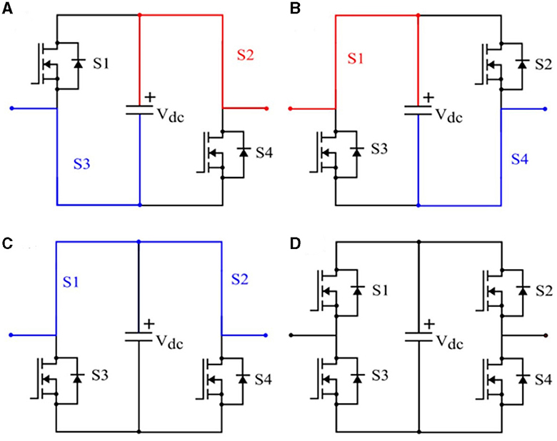
Figure 1. H-Bridge converter states of operation. (A) Positive output state (+Vdc). (B) Negative output state (+Vdc). (C) Bypass state (+0 V). (D) Off-state (Open Circuit).
Each H-bridge module can take on one of four states: a positive output state in which the module outputs +Vdc (Figure 1A), a negative output state in which the module outputs −Vdc (Figure 1B), a bypass state in which the module acts as a wire by bypassing the voltage source (Figure 1C), and an off-state in which the module acts as an open circuit (Figure 1D). The H-bridge converter is thus capable of outputting +Vdc, −Vdc, or +0 V (Fang et al., 2021c; Zhang et al., 2022). Note that there are two possible configurations for the bypass state: one in which switches S1 and S2 are turned on (as depicted in Figure 1C), and another in which switches S3 and S4 are turned on.
While existing multilevel converters allow for improved voltage ratings, current ratings are unaffected as each module still has to carry the entire current flow. To address this, multiple CBC arms can be connected in parallel. In addition, novel module topologies such as the double H-bridge have been investigated with the goal of allowing for some degree of parallel connectivity. However, these methods result in the loss of modularity and scalability, which are crucial benefits of multilevel converters. Thus, lattice converters have been proposed to facilitate both serial and parallel connectivity while preserving the benefits of modularity and scalability (Fang, 2021b).
While multilevel converters allow for one-dimensional (1D) scalability and modularity by allowing for connections between modules in one direction. Lattice converters aim to extend these benefits into the second and even third dimensions by allowing for connections between modules in the two-dimensional (2D) plane and in three-dimensional (3D) space (Fang, 2021b). In a lattice power grid, each grid-tied power converter acts as a submodule in a lattice structure. To better conceptualize and visualize these connections, we utilize graph theory modeling. With this model, the lattice power grid can be represented as a simple, undirected lattice graph in which each edge represents a module and each node represents an interconnection between two or more modules (Fang, 2021b; Mei et al., 2022; Zhang et al., 2022). Figure 2 depicts a square power grid and its lattice graph representation.
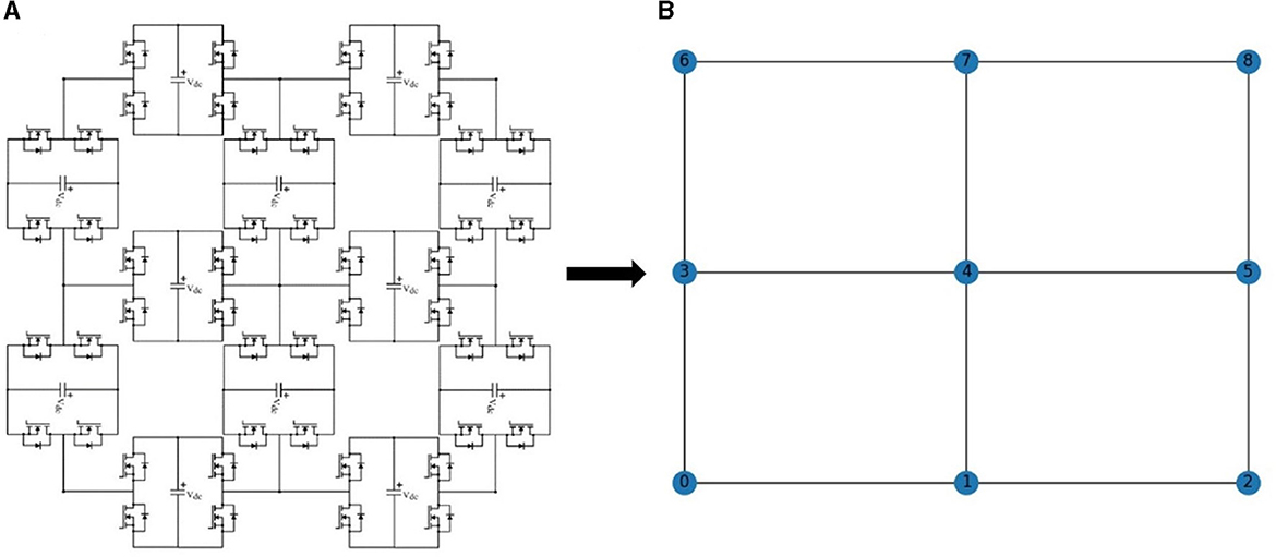
Figure 2. Square lattice power grid and its graph model. (A) Circuit schematic of a 3 × 3 square lattice power grid. (B) Graph model of 3 × 3 square lattice power grid.
The three regular tilings in the 2D plane are the square, triangular, and hexagonal tilings. The square, triangular, and hexagonal lattice power grids are based on these regular tilings. In addition, 2D lattice power grids based on Archimedean tilings and k-uniform tilings have also been proposed, as well as 3D lattices based on polyhedral tilings known as honeycombs (e.g., cubic honeycombs and Archimedean honeycombs) (Coxeter, 1973; Grünbaum and Shephard, 1977; Fang, 2021b). This article will focus on the three 2D regular tilings, but all the methods and algorithms discussed within it can be applied to any lattice power converter structure that can be represented using a simple, undirected graph.
A square lattice graph can be characterized by dimensions n, the number of nodes along its height, and m, the number of nodes along its width. Such a lattice graph is referred to as an “n×m square lattice graph.” As shown in Figure 1B, the bottom left node is numbered as 0, and the node number counts up from left to right. When the end of a row is reached, the leftmost node of the row immediately above is counted next. Under this scheme, the top right node in the lattice is given node number nm−1, the largest node number in the lattice (Zhang et al., 2022).
We can then characterize this lattice graph using an adjacency matrix. We can first define a nm×nm matrix Asq consisting of all zeroes. Then, we can construct the square lattice using the following process (Fang, 2021b):
1. Iterate through each element Asq(i, j), where i, j ∈ 1, 2, …, ñm.
2. If abs(i−j) = n, then set element Asq(i, j) = 1. This connects all vertical edges of the lattice graph.
3. If abs(i−j) = 1 and , then set Asq(i, j) = 1. This connects all horizontal edges of the lattice graph.
The resulting matrix is henceforth referred to as the “graph adjacency matrix,” or GAM, of the lattice graph. The GAM characterizes where modules physically exist and how they are interconnected. It should be distinguished from the “path adjacency matrix,” or PAM, which characterizes the operating states of each individual module (this is described in further detail in Section Control algorithms for single input/output operation).
Each edge can be identified by its two endpoints. For instance, the edge between Node 1 and Node 2 can be identified as “Edge 1–2” or “Module 1–2.”
If we offset each row of nodes in a triangular lattice graph as shown in Figure 3, the lattice can be made to lie on a square arrangement of nodes. Thus, we can use the same numbering scheme as in the square lattice graph. In fact, an m×n triangular lattice graph is simply an m×n square lattice graph with the addition of the diagonal edges in each square (Zhang et al., 2022). Two embodiments of the triangular lattice graph are shown. In a Type 1 triangular lattice, the diagonal edge connects the bottom left and top right nodes in each square (Figure 3A). In a Type 2 triangular lattice, the diagonal edge connects the top left and bottom right nodes in each square (Figure 3B).
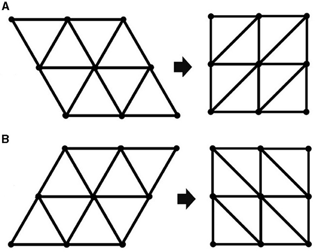
Figure 3. (A) Type 1 and (B) Type 2 triangular lattices and their equivalent transformations into square node arrangements.
We can again construct these graphs through adjacency matrices. To define the adjacency matrix Atr1 representing a Type 1 m×n triangular lattice graph:
1. Set Atr1 equal to Asq, where Asq is the square adjacency matrix of an m×n square lattice graph as constructed in Section Formation of square lattice graphs.
2. Iterate through each element Atr1(i, j), where i, j ∈ 1, 2, …, ñm.
3. If abs(i−j) = n+1 and , then set Atr1(i, j) = 1. This connects all diagonal edges of the graph.
To define adjacency matrix Atr2 representing a Type 2 m×n triangular lattice graph, we follow the same process with a modification to step 3:
1. Set Atr2 equal to Asq, where Asq is the square adjacency matrix of an m×n square lattice graph as constructed in Section Formation of square lattice graphs.
2. Iterate through each element Atr2(i, j), where i, j ∈ 1, 2, …, ñm.
3. If abs(i−j) = n−1 and , then set Atr2(i, j) = 1. This connects all diagonal edges of the graph.
Like triangular lattices, hexagonal lattices can also be mapped onto a square arrangement of nodes, as shown in Figure 4. Here, the lattice takes on a “bricklaying” pattern, in which all vertically adjacent pairs of nodes are connected while horizontally adjacent pairs of nodes alternate between being connected and unconnected both in the up-down and left-right directions (Zhang et al., 2022). Two embodiments of hexagonal lattices are defined. In a Type 1 hexagonal lattice, Nodes 0 and 1 are connected (Figure 4A). In a Type 2 hexagonal lattice, Nodes 0 and 1 are unconnected (Figure 4B).
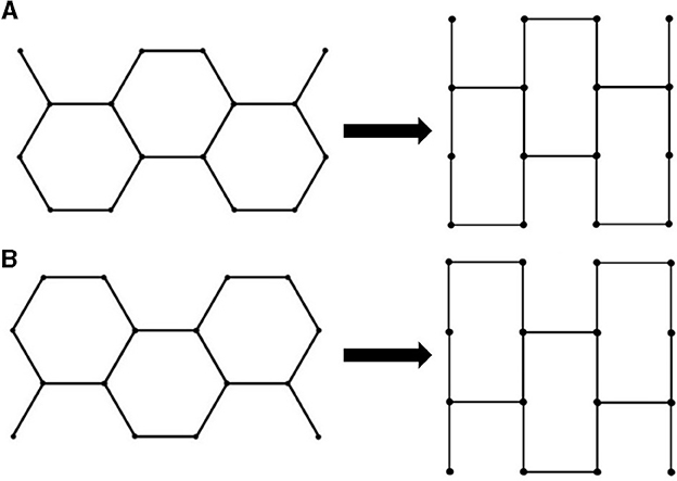
Figure 4. (A) Type 1 and (B) Type 2 hexagonal lattices and their equivalent transformations into square node arrangements.
We can again construct hexagonal lattices using adjacency matrices. Firstly, for an m×n lattice and Node i, let us define the functions col(i, n) and row(i, n). These functions return, respectively, the row number and column number that Node i lies in. Row 0 is defined as the bottom row of nodes, and column 0 is defined as the leftmost column of nodes.
a.
b.
To construct adjacency matrix Ahex1 for an m×n hexagonal lattice graph:
1. Set Ahex1 equal to Asq, where Asq is the square adjacency matrix of an m×n square lattice graph as constructed in Section Formation of square lattice graphs.
2. Iterate through each element Ahex1(i, j), where i, j ∈ 1, 2, …, ñm.
3. If row(i, n) = row(j, n), row(i, n)%2 = 0, and col(min(i, j), n)%2 = 1, then set Ahex(i, j) = 0. Here, % represents the modulo operator.
4. If row(i, n) = row(j, n), row(i, n)%2 = 1, and col(min(i, j), n)%2 = 0, then set Ahex(i, j) = 0.
The fundamental objective of the proposed control and optimization algorithm is to select any two nodes in the lattice (which can serve as input/output ports for electrical loads) and generate a desired voltage and current capacity between them. To generate a voltage of kVdc between two nodes, a path of length l≥k modules (edges) must be identified between them (Fang, 2021b; Mei et al., 2022; Zhang et al., 2022). Then, k modules along that path are switched to generate a voltage step of Vdc in the desired direction, and the remaining l−k modules in the path are switched to the bypass mode and do not contribute any voltage increase. In essence, this creates a serially connected cascaded-bridge converter between the two nodes.
As mentioned previously, one drawback of cascaded-bridge converters is that while they allow for the generation of high voltages, they suffer from limited current ratings as each module must bear the entire current. This necessitates the use of more robust and expensive components such as transistors, diodes, and DC voltage sources. Lattice power grids allow for an increase in current ratings by generating two or more paths in parallel between the end nodes, allowing for current sharing between the paths. This is analogous to connecting multiple CBCs in parallel.
Figure 5 depicts an example lattice state for a 4 × 4 square lattice power grid. In this lattice state, a voltage difference of +4Vdc has been generated between Nodes 4 and 7, with three parallel paths between them. In this figure, red edges denote modules that are outputting voltages, and the arrows denote the direction of the voltage increase (e.g., Node 5 is +Vdc higher than Node 4). Blue edges indicate modules in the shorted bypass state, and thin black edges denote modules in the OFF state, acting as open circuits.
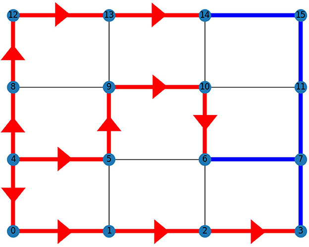
Figure 5. Example lattice state for a 4 × 4 square lattice power grid.
The secondary objective of the algorithm is to switch between lattice states in an efficient manner. For each set of parameters (end nodes, voltage increase, and number of parallel paths), there may be many lattice states that fulfill those parameters. The lattice state that is selected should be the one that minimizes the number of transistor switching actions. This allows for more efficient operation as switching losses are minimized, and the total noise generated from switching is reduced as well.
The pathfinding algorithm, named findPaths, is the first component of the overall control and optimization algorithm, and it seeks to identify all paths between two arbitrary nodes in a lattice graph of length l≥k, where +kVdc is the desired voltage difference. Only integer values of k need to be considered, as non-integer multiples of +Vdc can achieved using pulse-wave modulation. Furthermore, in order to preserve the efficiency of the algorithm and reduce its runtime, if a path length is >k, then the first k modules in the path are switched to an output state (+Vdcor −Vdc depending on directionality) and the last l−k modules are operated in the bypass state. While it would be valid to arrange the outputting modules and bypassed modules differently, considering every such arrangement would inject excessive complexity into the pathfinding algorithm.
Firstly, a graph adjacency matrix for the lattice graph is generated using the methods described in Section Fundamentals of lattice power converters. A Graph object is then generated from the GAM, where every node in the graph is associated with a list or array consisting of all its adjacent nodes. In Python, this can be implemented using the dictionary structure, where each node number is a key and the value associated with each key is the list of all adjacent nodes.
The findPaths algorithm is given a starting node and a destination node, and it then utilizes depth-first search (DFS) to traverse paths beginning at the starting node. If the destination node is encountered during traversal and the length of the path is >k, then the path is saved as a viable path. The algorithm then backtracks along the path and attempts to traverse a different path until all have been exhausted. When findPaths has finished running, it will have identified all viable paths between the start and destination nodes. DFS of a graph is very similar to DFS of a binary search tree, with one difference. In a graph, it is possible to revisit a node during traversal, resulting in endless or undesired loops. Thus, nodes that have already been visited are marked as such and cannot be traversed again. When the algorithm backtracks upon identifying a viable path, the backtracked nodes are marked as unvisited and can be traversed again (Yadav, 2021; Cormen et al., 2022).
Figure 6 depicts an example output of the pathfinding algorithm for a 2 × 2 type 1 triangular lattice graph. Node 0 is the starting node and Node 2 is the destination node, and a voltage difference of +Vdc is desired. Three viable paths have been identified by findPaths.
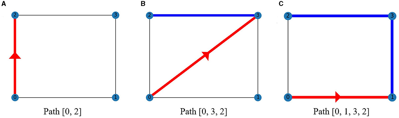
Figure 6. Example output of path-finding algorithm for a 2 × 2 square lattice. (A) Path [0, 2]. (B) Path [0, 3, 2]. (C) Path [0, 1, 3, 2].
The output of findPaths in this case would be the following list of lists: [(0, 2), (0, 3, 2), (0, 1, 3, 2)].
The parallel paths algorithm (called currentPaths) takes the output of findPaths as its input, which consists of a list of every viable path between the starting and destination nodes of sufficient length to satisfy current requirements. If p parallel paths are desired, then these viable paths are placed into every possible permutation of size p. In Python, these permutations can be implemented as size-p lists of lists. If v viable paths were outputted by findPaths and p parallel paths are desired, then the algorithm will process a total of path permutations. A path permutation is a viable solution if it satisfies the following:
1. There are no voltage conflicts between paths. That is, if two or more paths intersect each other at a node, then each path must yield the same voltage at that node. Otherwise, the intersection will result in a voltage conflict
2. No two paths can share an edge. If two paths were to share an edge, even in the absence of a voltage conflict, then the module represented by that edge would bear the combined current load of both paths, negating the purpose of the parallel paths algorithm. This results in an edge conflict.
If a voltage or edge conflict exists in a path permutation, then that permutation is discarded by currentPaths. Otherwise, the permutation is included in the output. The output of currentPaths is the list or set of all viable path permutations. This set consists of all end states that are valid solutions to the desired voltage and current parameters.
The goal of the switching loss optimization algorithm (called leastChanges) is to facilitate time-variant state changes of the lattice power grid in a manner that reduces the number of switching actions between lattice states. The parallel paths algorithm, currentPaths, outputs the set of all viable end states that fulfill the desired voltage and current parameters. From this set, the optimization algorithm selects one optimal end state to be implemented, where the optimality criteria is the similarity of the end state to the initial state. A greater similarity between the initial and end states means fewer switching actions (and thus lower switching losses) to change states.
The design of the switching loss optimization algorithm is as follows. For any lattice state, a path adjacency matrix (PAM) can be assigned, which identifies the operating state of each individual module in the lattice. This should not be confused with the graph adjacency matrix (GAM), which represents how modules are physically arranged and interconnects between nodes. Because each module can take on one of four operating states, each element of the PAM P can take on one of four values:
1. If module a-b is in the +Vdc state, then P(a, b) = 1
2. If module a-b is in the −Vdc state, then P(a, b) = − 1
3. If module a-b is in the bypass state, then P(a, b) = 0.01
4. If module a-b is in the OFF state, then P(a, b) = 0
We can establish a convention that a module is in the +Vdc operating state if the higher-numbered node is held at a higher voltage than the lower-numbered node. If the lower-numbered node is held at a higher voltage than the higher-numbered node, then the converter is in the −Vdc state. Note that if the two bypass states were replaced with each other, there would be no changes in the number of switching actions to and from other states. Thus, the two bypass states can be regarded as identical in the context of the switching loss optimization algorithm.
A previous version of the switching loss optimization algorithm treated all module-level state changes equally (Zhang et al., 2022). This updated algorithm is improved by accounting for the fact that switching between the positive output stage and the negative output state requires a total of four transistor switching actions: S1 and S4 must be turned OFF, while S2 and S3 are turned ON. Meanwhile, all other module state changes require just two switching actions. Thus, the updated algorithm analyzes transistor-level state changes rather than just module-level state changes.
The leastChanges algorithm first generates PAMs for the initial lattice state as well as all the potential end states outputted by currentPaths. If the lattice power grid is initially OFF, then the initial PAM is a matrix consisting of all zeroes. The end state PAMs are each compared with the initial state PAM and the number of transistor-level state changes is counted. A simple example of this comparison is shown for a 2 × 2 square lattice in Figure 7. The transition from Pinit(0, 1) = 1 to Pend(0, 1) = 0 contributed two switching actions, while the transition from Pinit(1, 3) = 1 to Pend(1, 3) = −1 contributed four switching actions. As the P(a, b) represents the same module as P(b, a), elements below the diagonal of the matrix can be disregarded to avoid redundancy. Thus, a total of six switching actions were required to make the state change shown in Figure 7. Upon comparing the initial state PAM with every potential end state PAM, the optimization algorithm converges upon the end state with the smallest number of switching actions, which is deemed to be the most efficient and is implemented.
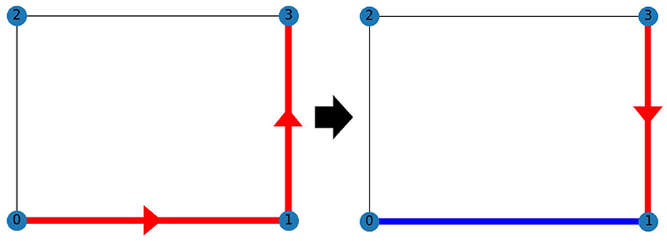
Figure 7. Example of a lattice state change between an initial state (Left) and an end state (Right).
In summary, the components of the single input/output control and optimization algorithm are integrated and operated in the following manner. The algorithm takes in seven inputs: lattice type, lattice height, lattice width, starting node, destination node, desired voltage increase, and desired current capacity. The pathfinding algorithm findPaths generates a graph adjacency matrix using the lattice type and dimensions, and then utilizes depth-first search to identify all paths between the starting and ending node of a sufficient length to support the desired voltage increase. These viable paths are inputted into the parallel paths algorithm currentPaths, which generates path permutations with enough parallel branches to support the desired current capacity. The switching loss optimization algorithm leastChanges then compares each of these path permutations with the initial lattice state to determine which one requires the smallest number of switching actions and is thus the most efficient. New voltage and current parameters can be input continuously on a loop and these steps can be repeated indefinitely to allow for the continuous single input/output operation of the lattice power grid.
The algorithms discussed in Section Control algorithms for single input/output operation involved single input/output operation of the lattice power grid; there was one starting node and one destination node. To allow for increased flexibility and versatility, this section introduces the multiple input/output operation of lattice power grids. A pair of end nodes and the parallel paths between them are referred to as a “path permutation” as described in Section Achieving current objectives through parallel paths. A path permutation satisfies a single set of parameters, consisting of end node locations, voltage difference, and current capacity. Multiple input/output operation seeks to implement more than one path permutations on the same lattice graph, with multiple pairs of end nodes. These path permutations satisfy separate voltage and current requirements and can thus be used to drive two or more loads independently of each other.
We propose and implement three modes of multiple input/output operation. Firstly, sequential operation allows for the addition or removal of single path permutations one by one to the lattice graph. In contrast, simultaneous operation allows for multiple path permutations to be added onto the lattice at the same time. Finally, the two can be integrated into combined sequential-simultaneous operation, in which sets of simultaneous path permutations can be added or removed from the lattice in a sequential manner.
Sequential operation involves placing a new path permutation on some initial lattice state in which path permutations may already exist on the lattice graph. Figure 8 depicts an example of sequential operation, in which a new path permutation with starting Node 3 and destination Node 5 is placed onto a 3 × 3 square lattice graph with a preexisting path permutation.
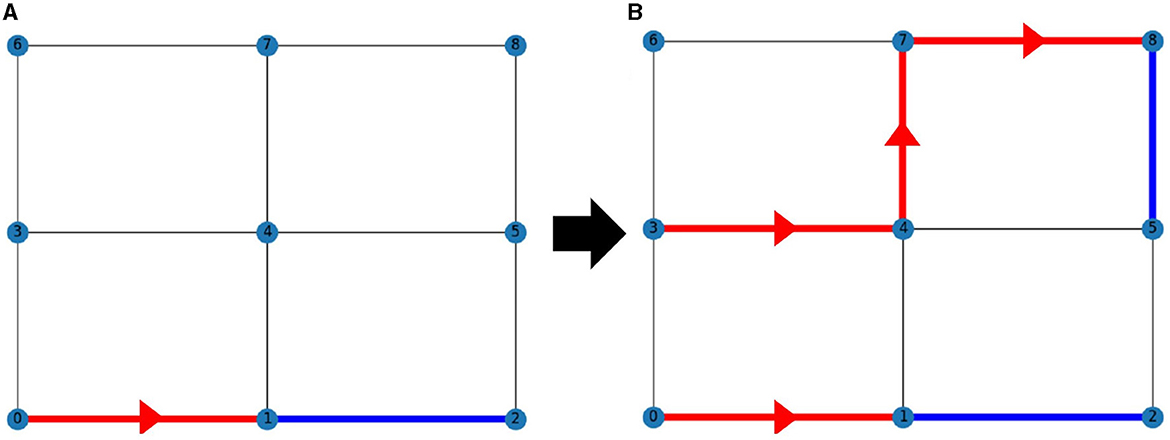
Figure 8. Sequential operation of a lattice power grid. (A) Initial state with pre-existing path permutation. (B) End state.
During multiple input/output operation, the connected loads should be driven independently from one another, so separate path permutations should not share any nodes or edges with each other. Thus, the sequential operation algorithm, named mioSequential, works by first disconnecting any nodes in the initial lattice state that are traversed an existing path, and then applying the single input/output algorithms on the remaining lattice to generate the new path permutation.
To accomplish this, mioSequential first identifies all nodes traversed by a path in the initial lattice state. For the state shown in Figure 8A, this includes Node 0, Node 1, and Node 2. Then, a copy is made of the graph adjacency matrix of the lattice, and the rows and columns associated with the traversed nodes are set to zero. This effectively removes these nodes from the lattice along with any edges that are adjacent to it. For example, the GAM representing Figure 8A, Ainit , (i.e., the GAM of a 3 × 3 square lattice graph) is given by the following:
The GAM used to generate Figure 8B, Gseq, is derived by setting rows 0, 1, and 2 as well as columns 0, 1, and 2 to zero.
The modified GAM can then be used by the single input/output algorithms findPaths, currentPaths, and leastChanges to determine a new path permutation on the remaining parts of the lattice, in the same way as described in Section Control algorithms for single input/output operation. Once the new path permutation is determined, it is added to the original lattice state so that all nodes, edges, and paths are included. The initial state is then updated for the next execution of the sequential operation algorithm.
The mioSequential algorithm also allows for the sequential deletion of paths as well. If the user opts for deletion and inputs a node number, then mioSequential will remove any path that traverses the inputted node from the initial state. This is done by switching all modules along the deleted path to the OFF state. The path adjacency matrix associated with the lattice state is modified accordingly.
Simultaneous operation involves simultaneously placing multiple path permutations with independent parameters. To introduce the concept, let us first consider the case in which each path permutation only consists of one single path; in other words, the requirement of parallel paths is dropped for now. The simultaneous placement of multiple independent paths is similar in principle to the placement of parallel paths. The goal of the parallel paths algorithm currentPaths was to place multiple paths that started and ended on the same two nodes, whereas now we wish to place multiple paths that start and end on different pairs of nodes. Thus, we replace the permutations of currentPaths with Cartesian products.
The Cartesian product of two sets A and B is the set of all ordered pairs (a, b) where a ∈ A and b ∈ B (Weisstein, 2022). This concept can be generalized to the n-ary Cartesian product of n sets X1, X2, …, Xn, which is defined as the set of all tuples (x1, x2, …, xn), where x1 ∈ X1, x2 ∈ X2, …, xn ∈ Xn.
For this application, X1, X2, …, Xn are the sets of all viable paths that fulfill the parameter sets p1, p2, …, pn, respectively. Each parameter set contains the starting node location, destination node location, and minimum path length (recall that parallel paths are disregarded for now). The path sets X1, X2, …, Xn are found by running each of p1, p2, …, pn through the pathfinding algorithm findPaths as described in Section Achieving voltage objectives through pathfinding. So, in order to fulfill all n sets of parameters, one path must be taken from each path set and implemented. When one path is taken from each set and combined into a tuple, the result is an element of the Cartesian product X1× X2×… × Xn. In fact, X1× X2×… × Xn is the set of all tuples that can be created in such a manner. The number of elements in the Cartesian product is given by n(X1) × n(X2) × … × n(Xn), where n(Xi) returns the number of elements in Xi (i.e., its cardinality). However, in our application, the order of the paths in the tuples is not relevant, so this number is reduced by a factor of n!. In other words, tuples that contain the same paths but in a different order are not considered unique.
The simultaneous operation algorithm, named mioSimultaneous, then analyzes all unique path tuples in the Cartesian product X1× X2×… × Xn and checks for any path intersections (i.e., common nodes). If any intersections exist in a path tuple, then it is considered invalid and is thrown out. If no intersections exist, then the path tuple is a valid solution to the parameter set p1, p2, …, pn.
We can consider a simple example for a 2 × 2 square lattice. Suppose that we wish to find a path from Node 0 to Node 1 and another path from Node 2 to Node 3 with voltage differences of +VDC for both. Let X1 and X2 be the tuples of all paths that satisfy the first parameter set and second parameter set, respectively. We have X1 = ([0, 1], [0, 2, 3, 1]) and X2 = ([2, 3], [ 2, 0, 1, 3]).
The Cartesian product of the two sets is the following:
Of the path tuples in this Cartesian product, only the first, ([0, 1], [2, 3]) contains no path intersections and is thus a valid state.
Now, we reintroduce the requirement of parallel paths. To allow for p parallel paths that each satisfy the parameter set pi, we simply duplicate the path set Xi by p times. Then, the algorithm determines the Cartesian product of X1, X2, …,Xi1, Xi2, …, Xip, …, Xn, where Xi = Xi1 = Xi2 = … = Xip. As a result, each path tuple in the Cartesian product will contain p paths that satisfy the parameter set pi. To allow for paralleling, paths that intersect only at the starting and destination nodes are no longer to be conflicting. Figure 9 depicts an output of mioSimultaneous that involves parallel paths.
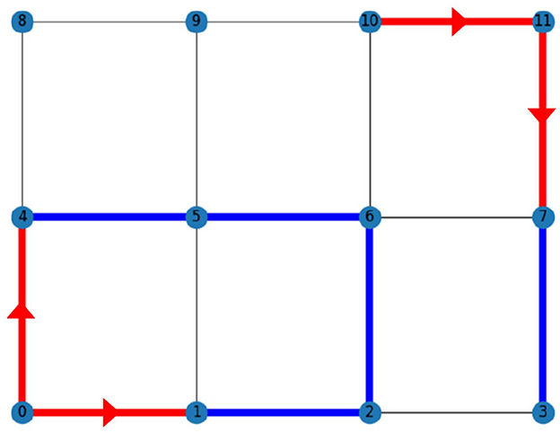
Figure 9. Example output of simultaneous operation algorithm with parallel paths.
There may be more than one path tuple that fulfill all the requested parameter sets. Again, the switching loss optimization algorithm leastChanges is used to select the one that requires the smallest number of transistor switching actions. This process is identical to the one discussed in Section Optimization algorithm for switching loss reduction: a path adjacency matrix is generated for each viable path tuple, and each is compared to the PAM of the initial lattice state to determine the number of transistor switching actions.
The final version of the proposed algorithm, mioCombined, combines both sequential and simultaneous operation. Whereas, under sequential operation only one path permutation could be added to the lattice on each loop (i.e., one set of parallel paths), the combined operation algorithm allows the simultaneous addition of multiple independent path permutations on each loop. As in sequential operation, each loop of the combined operation algorithm removes traversed nodes from the lattice by setting their associated rows and columns in the GAM to zero. Then, the simultaneous operation algorithm, mioSimultaneous, is run on the remaining portion of the lattice to generate new paths. The removed nodes, along with the initially existing paths, are then re-added to the lattice to construct the complete lattice state. This process can be repeated indefinitely using a while loop.
A flowchart depicting the structure of the complete control and optimization algorithm for combined sequential-simultaneous operation is included in Figure 10.
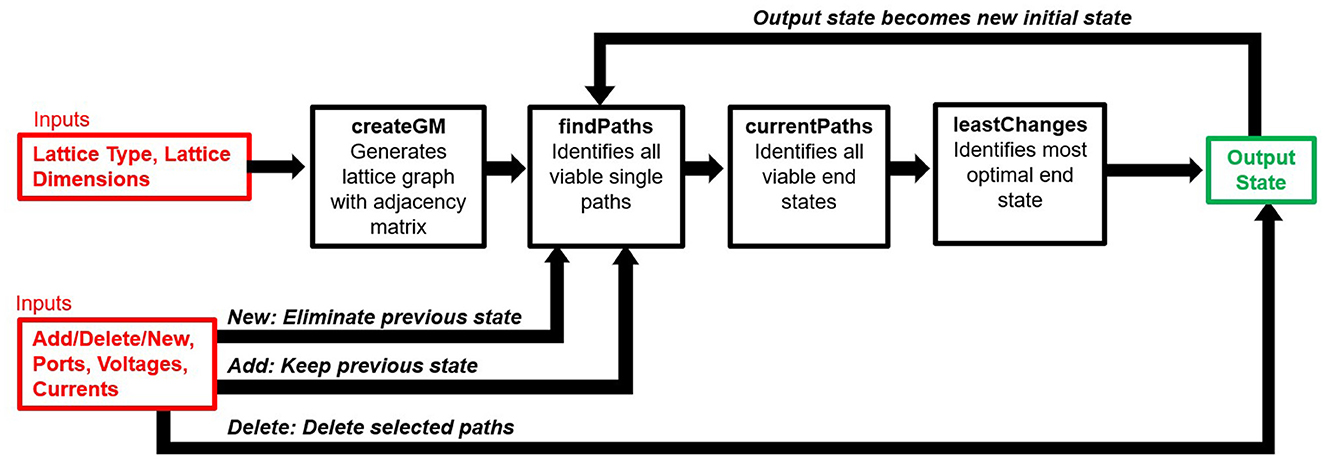
Figure 10. System model of the proposed algorithm.
On each loop, the user is presented with three options: add paths, find new lattice state, or delete paths. The first option allows for new paths to be added while preserving already-existing paths in the lattice state. The second option removes all existing paths and turns all modules OFF, allowing for new paths to be generated on a clean slate. Finally, the third option allows for the user to enter a node number, and any path that traverses that node is removed.
Let us perform this algorithm on a 3 × 3 Type 1 triangular lattice grid (Figure 11). On the first loop, the “add paths” and “find new lattice state” options are functionally the same as all modules are initially OFF. Firstly, we simultaneously add two path parameters: one starting at Node 0 and ending at Node 4 with a voltage difference of +Vdc and three parallel paths, and another starting at Node 2 and ending at Node 8 with a voltage difference of +2Vdc and one parallel path.
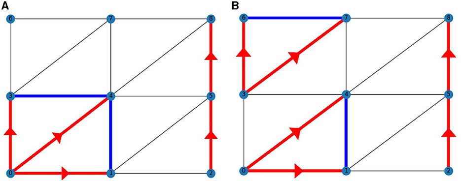
Figure 11. Example output of combined sequential-simultaneous operation algorithm after: (A) simultaneous path generation (B) path deletion and sequential path generation.
The lattice state is then plotted and shown in Figure 11A. Fourteen transistor-level switching actions were required to reach this lattice state.
The algorithm repeats in a loop, and the user is again presented the option to add paths, find a new lattice state, or delete paths. Let us delete the path that traverses Node 3. Lastly, let us add a new path permutation with a voltage difference of +Vdc and two parallel paths between Nodes 3 and 7 to the lattice state while preserving the existing paths. The updated lattice state is plotted in Figure 11B.
Simulations of the lattice power grid in multiple input/output operation were performed in the MATLAB/Simulink environment. A 3 × 4 triangular lattice power grid was built in Simulink, utilizing “Full-Bridge Converter” blocks to model the 23 H-bridge modules (MathWorks., 2021). The path adjacency matrix outputted by the control and optimization algorithm was used to generate the 23 gating signals for the modules. Each module contains a 1 kV DC voltage source.
The proposed algorithms were used to generate the lattice state shown in Figure 12. It consists of one path permutation between Nodes 0 and 10 with voltage difference +2Vdc and two parallel paths, and another between Nodes 2 and 11 with voltage difference +3Vdc and one parallel path. This lattice state was then realized on the Simulink model. An RL load with a resistance of 500 Ω and an inductance of 11 μH was connected between Nodes 0 and 10, and an identical load was connected between Nodes 2 and 11. The currents and voltages across these loads were measured over time and plotted in Figure 13.
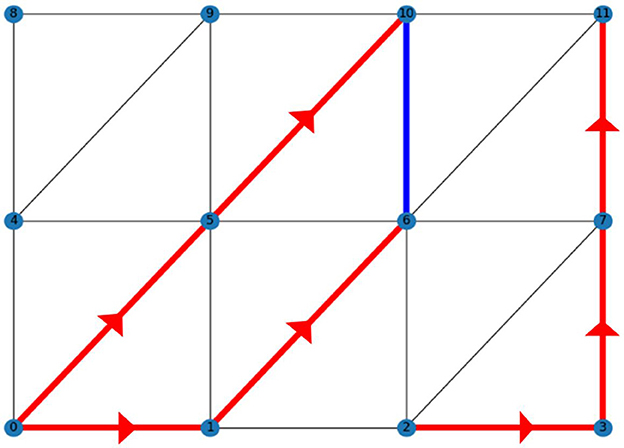
Figure 12. Generated lattice state for DC analysis.
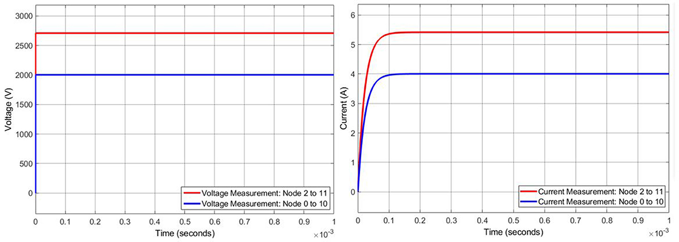
Figure 13. Measured voltage and current under DC analysis.
Across Nodes 0 and 10, the voltage difference approaches 2 kV and the current approaches 4 A, which is expected given the inputted parameters and Ohm's Law. Between Nodes 1 and 11, the voltage difference approaches 2.71 kV and the current approaches 5.42 A. These values are lower than expected. The reason is the large voltage differences between nodes the two path permutations, especially between Nodes 10 and 11. Even though converter 10–11 is switched OFF, the large voltage across it causes leakage that pulls down the voltage at Node 11. This is confirmed by the fact that when the modules between the two path permutations are removed and replaced with open circuits, the voltage between Nodes 10 and 11 rises to 3 kV as expected. Thus, the off-state voltage ratings and leakages across nodes are issues that ought to be accounted for in the design and operation of physical lattice power grids.
One of the most significant benefits of the lattice converters is its flexibility and versatility. While two resistive loads were driven simultaneously by the lattice converter in the previous simulation, the multiple input/output nodes in a lattice state can also be used to repeatedly drive a single load. One potential application of this is as a stimulator for a transcranial magnetic stimulation (TMS) device, in which very large currents are driven through an inductor coil to generate a magnetic field strong enough to stimulate neurons (Peterchev and Murphy, 2013; Chail et al., 2018; Zeng et al., 2022). It is often desirable to generate pulse trains (paired-pulse, triple-pulse, quadripulse, etc.) with short intervals of less than a millisecond, which can be difficult for existing TMS stimulator topologies utilizing traditional two-level converters or even multilevel converters (Goetz et al., 2012; Li et al., 2022; Zeng et al., 2022). A TMS stimulator based on a lattice converter would allow for the convenient and flexible generation of pulse trains.
TMS topologies based on one-dimensional multilevel converters have been previously developed (Zeng et al., 2022), greatly improving the controllability of pulse shape, width, and amplitude while allowing for briefer, faster, and higher-frequency pulse generation (in comparison to conventional single-module TMS topologies). A TMS topology based on a lattice converter with parallel connectivity has the potential to further improve speed and controllability and introduces the possibility of current sharing across modules. This reduces the current burden on each module and allows for simpler and more affordable components to be used, including storage capacitors, snubber capacitors and resistors, relays, and discharge boards.
We will model this using the same 3 × 4 triangular lattice grid as in Section Simulations. The TMS inductor coil is modeled by an inductor component of inductance 11.7 μH. We can generate a paired pulse by using two path permutations of the same voltage and connecting the inductor coil to both sets of input and output nodes. The lattice state shown in Figure 14 was generated by the control and optimization algorithm. Both path permutations feature two parallel paths to allow for increased current capacity. One end of the inductor coil is connected to both Nodes 1 and 4, while the other end is connected to Nodes 7 and 10.
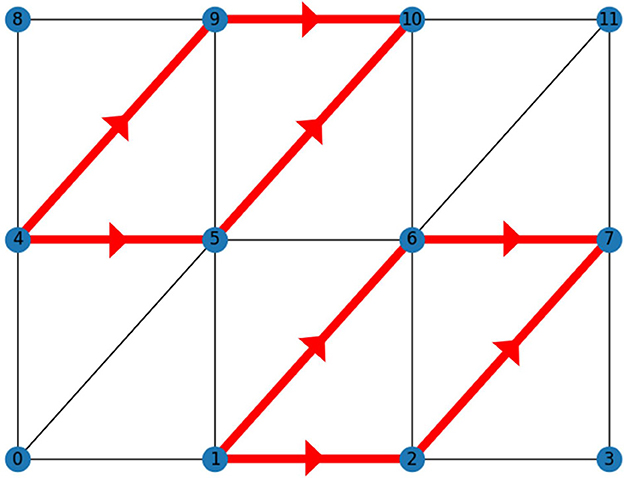
Figure 14. Lattice state used to generate stimulate TMS pulses.
The voltage generated across the inductor coil controls the derivative of the current through it. A positive coil voltage will cause current to increase at a constant rate, and a negative voltage will cause current to decrease. Thus, a monophasic pulse can be generated by first switching one path permutation on for a period of time and then reversing the voltage for the same period. The second pulse is generated by doing the same to the second path permutation. Pulse trains consisting of more pulses (e.g., triple-pulse or quadri-pulse) could be generated by increasing the number of path permutations in the lattice state and connecting the input/output nodes to the inductor coil. A monophasic paired pulse with a 600 μs interval is shown in Figure 15A.
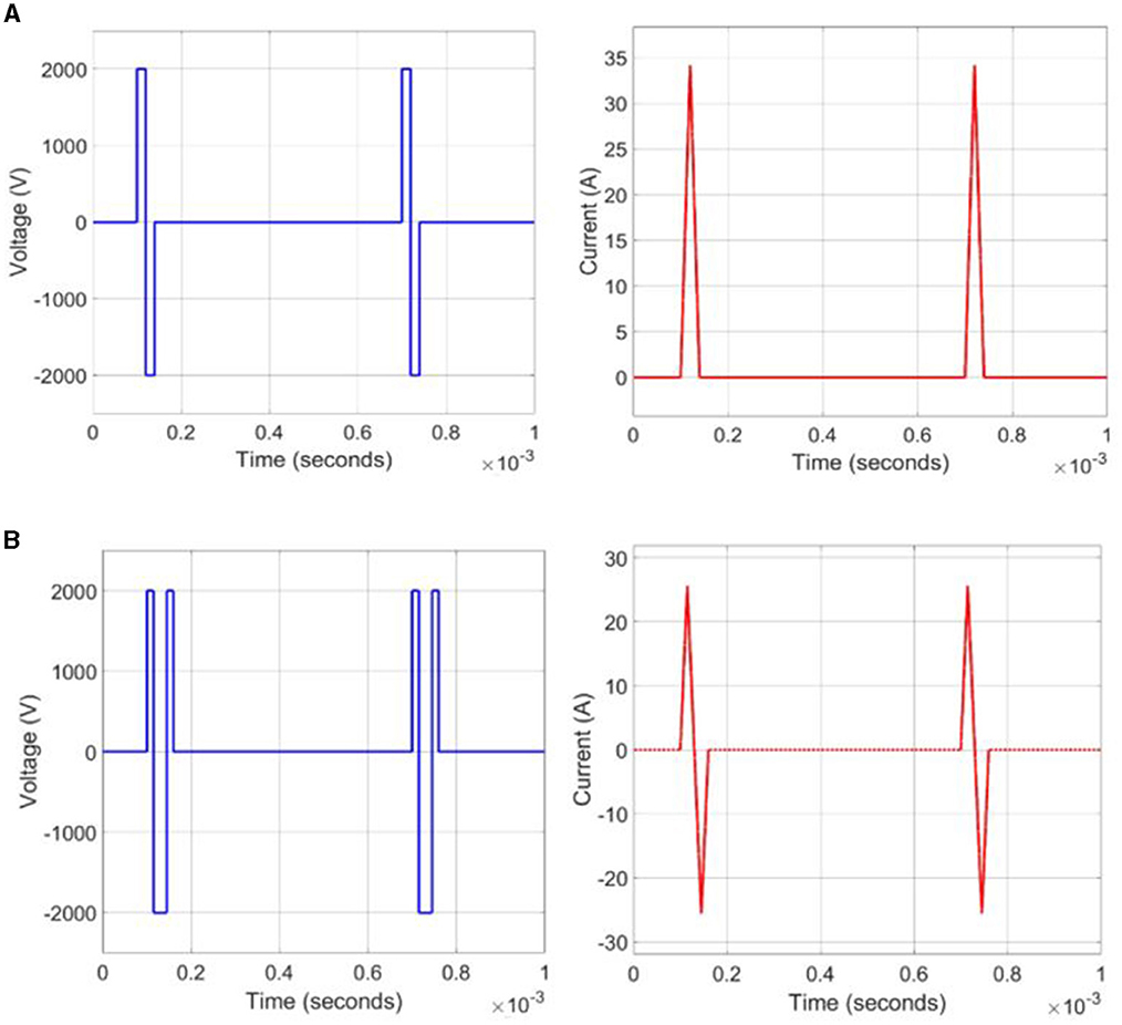
Figure 15. (A) Simulated voltage and current waveforms for monophasic paired-pulse train. (B) Simulated voltage and current waveforms for biphasic paired-pulse train.
A biphasic pulse can be generated by first generating a positive coil voltage for some time period tp, reversing the voltage for time 2tp, then switching back to a positive voltage for another period tp. A biphasic paired pulse with a 600 μs interval is shown in Figure 15B.
In addition to monophasic and biphasic pulses generated using rectangular voltage pulses, a wide variety of pulse shapes can be generated using the improved controllability of modular voltage stimulators. Sinusoidal monophasic and biphasic pulses can be generated with cosinusoidal voltage pulses, and polyphasic pulses can be generated with a Gaussian envelope (Li et al., 2022; Zeng et al., 2022). As lattice converters inherit the pulse controllability of one-dimensional multilevel converters, the generation of more unique and complex TMS pulse types is a promising direction for future exploration of TMS topologies based on lattice converters.
This work is the first implementation and demonstration of a control algorithm for the lattice grid topology which allows for multiple input/output operation. Control and optimization methodologies previously proposed by Zhang et al. (2022) and Mei et al. (2022) allow for only single input/output operation; those results only allow for the lattice grid to interface with one load or grid-connected device at a time. The same is true for the experimental results in Fang et al. (2023), which demonstrates the use of a lattice converter as an inverter, but only for one load. A technique for basic multiple input/output operation was described theoretically in Fang (2021b), but it did not account for paralleled paths or simultaneous operation. The algorithms proposed in this paper allow for the greatest access to the benefits of multiple input/output operation, introducing three possible modes of operation and maintaining the benefits of parallel connectivity. Thus, the proposed algorithms provide the greatest degree of versatility in both grid-connected interactions and standalone operation, and the results of Simulations and Using multiple input/output operation to drive loads repeatedly represent the first simulated demonstrations of multiple input/output operation in a lattice grid.
This article proposes new control and optimization algorithms for the operation of lattice power grids. Lattice power grids combine the benefits of serial and parallel connectivity, allowing for both high-voltage and high-current applications while maintaining the benefits of modularity and scalability. The concept of multiple input/output operation is proposed and implemented, allowing for increased flexibility and versatility in the applications of lattice power grids. These algorithms allow for voltage and current objectives to be achieved across input and output nodes in the converter, and multiple loads can be driven independently using multiple input/output node pairs. Finally, simulation results validate the proposed algorithms while raising the importance of accounting for voltage ratings and leakages in the design of physical lattice power grids. The generation of current pulses in transcranial magnetic stimulation is proposed as a potential application of lattice power converters.
The original contributions presented in the study are included in the article/supplementary material, further inquiries can be directed to the corresponding authors.
DZ contributed to the development of the mathematical model, coded and simulated the algorithm, and was responsible for preparing the bulk of the manuscript. JF contributed to the original concept of the lattice power grid, contributed to the development of the mathematical model, provided significant guidance to DZ, and reviewed and edited the manuscript. SG contributed to the original concept of the lattice power grid, provided significant guidance to DZ, and reviewed and edited the manuscript. All authors contributed to the article and approved the submitted version.
This work was partially supported by Jinan Municipal Government under Grant 20 New University Items, Grant Number 202228069, the National Natural Science Foundation of China under Grant Excellent Young Scientists Funding Program (Overseas), Grant Number 20221017-9, the Guangdong Basic and Applied Basic Research Foundation under Grant Guangdong-Shenzhen Joint Youth Fund, Grant Number 2022A1515110422, the Ministry of Science and Technology, PRC under Grant High-End Foreign Expert Recruitment Program, Grant Number G2022150006L, and Shandong University under Grant Distinguished Young Scholars Project, Grant Number 31400082260522.
The authors declare that the research was conducted in the absence of any commercial or financial relationships that could be construed as a potential conflict of interest.
The author JF declared that they were an editorial board member of Frontiers, at the time of submission. This had no impact on the peer review process and the final decision.
All claims expressed in this article are solely those of the authors and do not necessarily represent those of their affiliated organizations, or those of the publisher, the editors and the reviewers. Any product that may be evaluated in this article, or claim that may be made by its manufacturer, is not guaranteed or endorsed by the publisher.
Barros, L. A. M., Martins, A. P., and Pinto, J. G. (2022). A comprehensive review on modular multilevel converters, submodule topologies, and modulation techniques. Energies 15:1078. doi: 10.3390/en15031078
Blaabjerg, F., Chen, Z., and Kjaer, S. B. (2004). Power electronics as efficient interface in dispersed power generation systems. IEEE Trans. Power Electron. 19, 1184–1194. doi: 10.1109/TPEL.2004.833453
Chail, A., Saini, R. K., Bhat, P. S., Srivastava, K., and Chauhan, V. (2018). Transcranial magnetic stimulation: a review of its evolution and current applications. Ind Psychiatry J. 27, 172–180. doi: 10.4103/ipj.ipj_88_18
Chappell, B. (2021). “Renewable Energy Growth Rate up 45% Worldwide in 2020. IEA Sees New Normal.” National Public Radio. Available online at: https://www.npr.org/2021/05/11/995849954/renewable-energy-capacity-jumped-45-worldwide-in-2020-iea-sees-new-normal (accessed September 28, 2022).
Cormen, T. H., Leiserson, C. E., Rivest, R. L., and Stein, C. (2022). Introduction to Algorithms, Fourth Edition. MIT Press and McGraw-Hill. ISBN 0-262-04630-X. Section 20.3: Depth-first search, 563-572.
Denholm, P., Mai, T., Kenyon, R. W., Kroposki, B., and O'Malley, M. (2020). Inertia and the Power Grid: A Guide Without the Spin. Golden, CO: National Renewable Energy Laboratory. NREL/TP-6120-73856.
Erickson, R. W., and Maksimovic, D. (2001). Fundamentals of Power Electronics. Norwell, Mass, Kluwer Academic. doi: 10.1007/b100747
Fang, J. (2021a). More-Electronics Power Systems: Power Quality and Stability. Singapore: Springer Nature Singapore Pte Ltd. doi: 10.1007/978-981-15-8590-6
Fang, J. (2021b). Unified Graph Theory-Based Modeling and Control Methodology of Lattice Converters. Electronics. 10:2146. doi: 10.3390/electronics10172146
Fang, J., Blaabjerg, F., Liu, S., and Goetz, S. (2021a). A review of multilevel converters with parallel connectivity. IEEE Trans. Power Electron. 36, 12468–12489. doi: 10.1109/TPEL.2021.3075211
Fang, J., Gao, F., and Goetz, S. M. (2023). Symmetries in power electronics and lattice converters. IEEE Transac. Power Electron. 38, 944–955. doi: 10.1109/TPEL.2022.3195300
Fang, J., Li, H., Tang, Y., and Blaabjerg, F. (2019). On the inertia of future more-electronics power systems. IEEE J. Emerg. Select. Topic. Power Electron. 7, 2130–2146. doi: 10.1109/JESTPE.2018.2877766
Fang, J., Li, Z., and Goetz, S. M. (2021b). Multilevel converters with symmetrical half-bridge submodules and sensorless voltage balance. IEEE Trans. Power Electron. 36, 447–458. doi: 10.1109/TPEL.2020.3000469
Fang, J., Yang, S., Wang, H., Tashakor, N., and Goetz, S. (2021c). Reduction of MMC capacitances through parallelization of symmetrical half-bridge submodules, IEEE Trans. Power Electron. 36, 8907–8918. doi: 10.1109/TPEL.2021.3049389
Goetz, S. M., Li, Z., Liang, X., Zhang, C., Lukic, S. M., and Peterchev, A. V. (2017). Control of modular multilevel converter with parallel connectivity – application to battery systems. IEEE Trans. Power Electron. 32, 8381–8392. doi: 10.1109/TPEL.2016.2645884
Goetz, S. M., Peterchev, A. V., and Weyh, T. (2015). Modular multilevel converter with series and parallel module connectivity: topology and control. IEEE Trans. Power Electron. 30, 203–215. doi: 10.1109/TPEL.2014.2310225
Goetz, S. M., Pfaeffl, M., Huber, J., Singer, M., Marquardt, R., and Weyh, T. (2012). “Circuit topology and control principle for a first magnetic stimulator with fully controllable waveform,” in 2012 Annual International Conference of the IEEE Engineering in Medicine and Biology Society (San Diego, CA), 4700–4703. doi: 10.1109/EMBC.2012.6347016
Grünbaum, B., and Shephard, G. (1977). Tilings by regular polygons. Math. Mag. 50, 227–247. doi: 10.1080/0025570X.1977.11976655
Guo, F., and Sharma, R. (2015). “A modular multilevel converter with half-bridge submodules for hybrid energy storage systems integrating battery and ultracapacitor,” in 2015 IEEE Applied Power Electronics Conference and Exposition (APEC) (Charlotte, NC). doi: 10.1109/APEC.2015.7104783
Ilves, K., Taffner, F., Norrga, S., Antonopoulos, A., Harnefors, L., and Nee, H. (2015). A submodule implementation for parallel connection of capacitors in modular multilevel converters. IEEE Trans. Power Electron. 30, 3518–3527. doi: 10.1109/TPEL.2014.2345460
Lei, Y., Qin, S., Moon, I., Chou, D., Ye, Z., and Pilawa-Podgurski, R. C. N. (2017). A 2 kW, single-phase, 7-level flying capacitor multilevel inverter with an active energy buffer. IEEE Trans. Power Electron. 32, 8570–8581. doi: 10.1109/TPEL.2017.2650140
Li, Z., Lizana, R., Sha, S., Yu, Z., Peterchev, A. V., and Goetz, S. M. (2019). Module implementation and modulation strategy for sensorless balancing in modular multilevel converters. IEEE Trans. Power Electron. 34, 8405–8416. doi: 10.1109/TPEL.2018.2886147
Li, Z., Zhang, J., Peterchev, A. V., and Goetz, S. M. (2022). Modular pulse synthesizer for transcranial magnetic stimulation with flexible user-defined pulse shaping and rapidly changing pulses in sequences. arXiv:2202.06530v1. doi: 10.1088/1741-2552/ac9d65
Lin, Y. (2020). Research Roadmap on Grid-Forming Inverters. Golden, CO: National Renewable Energy Laboratory. Available online at: https://www.nrel.gov/docs/fy21osti/73476.pdf
Martinez-Rodrigo, F., Ramirez, D., Rey-Boue, A. B., De Pablo, S., and Herrero-de Lucas, L. C. (2017). Modular multilevel converters: control and applications. Energies 10:1709. doi: 10.3390/en10111709
MathWorks. (2021). Full-Bridge Converter. mathworks.Com. Available online at: https://www.mathworks.com/help/physmod/sps/powersys/ref/fullbridgeconverter.html (accessed June 27, 2021).
Mei, Z., Fang, J., and Goetz, S. (2022). Control and optimization of lattice converters. Electronics. 11:594. doi: 10.3390/electronics11040594
Peterchev, A. V., and Murphy, D. L. (2013). “Controllable pulse parameter transcranial magnetic stimulator with enhanced pulse shaping,” in 2013 6th International IEEE/EMBS Conference on Neural Engineering (NER) (San Diego, CA), 121–124. doi: 10.1109/NER.2013.6695886
Rohner, S., Bernet, S., Hiller, M., and Sommer, R. (2010). Modulation, losses, and semiconductor requirements of modular multilevel converters. IEEE Trans. Indus. Electron. 57, 2633–2642. doi: 10.1109/TIE.2009.2031187
Schon, A., Birkel, A., and Bakran, M. (2014). “Modulation and losses of modular multilevel converters for HVDC applications. PCIM Europe 2014,” in International Exhibition and Conference for Power Electronics, Intelligent Motion, Renewable Energy and Energy Management (Nuremberg).
Song, G., Cao, B., and Zhang, L. (2022). Review of grid-forming inverters in support of power system operation. Chin. J. Electr. Eng. 8, 1–15. doi: 10.23919/CJEE.2022.000001
Tashakor, N., Bagheri, E., and Goetz, S. (2020). Modular multilevel converter with sensorless diode-clamped balancing through level-adjusted phase-shifted modulation. IEEE. Trans Power Electron. 36, 7725–7735. doi: 10.1109/TPEL.2020.3041599
Weisstein, E. W. (2021). Lattice Graph. Wolfram Mathworld. Available online at: https://mathworld.wolfram.com/LatticeGraph.html (accessed August 5, 2021).
Weisstein, E. W. (2022). Cartesian Product. Wolfram Mathworld. Available online at: https://mathworld.wolfram.com/LatticeGraph.html (accessed July 30, 2022).
Xu, J., Li, J., Zhang, J., Shi, L., Jia, X., and Zhao, C. (2019). Open-loop voltage balancing algorithm for two-port full-bridge MMC-HVDC system. Int. J. Electr. Power Energy Syst. 109, 259–268. doi: 10.1016/j.ijepes.2019.01.032
Yadav, N. (2021). Depth First Search or DFS for a Graph. geeksforgeeks.org. Available online at: https://www.geeksforgeeks.org/depth-first-search-or-dfs-for-a-graph (accessed September 28, 2022).
Zeng, Z., Koponen, L. M., Hamdan, R., Li, Z., Goetz, S. M., and Peterchev, A. V. (2022). Modular multilevel TMS device with wide output range and ultrabrief pulse capability for sound reduction. J. Neural Eng. 19, 1–16. doi: 10.1088/1741-2552/ac572c
Zhang, D. W., Fang, J., and Goetz, S. M. (2022). Control and optimization algorithms for lattice power grids with multiple grid-forming converters. Front. Energy Res. 10:878592. doi: 10.3389/fenrg.2022.878592
Keywords: lattice power grids, lattice converters, H-bridge converters, multilevel converters, graph theory
Citation: Zhang D, Fang J and Goetz S (2023) Control and optimization algorithm for lattice power grids with multiple input/output operation for improved versatility. Front. Smart Grids 2:1241963. doi: 10.3389/frsgr.2023.1241963
Received: 18 June 2023; Accepted: 31 July 2023;
Published: 17 August 2023.
Edited by:
Muhammad Babar Rasheed, University of Alcalá, SpainReviewed by:
Mohammed Ali Khan, University of Southern Denmark, DenmarkCopyright © 2023 Zhang, Fang and Goetz. This is an open-access article distributed under the terms of the Creative Commons Attribution License (CC BY). The use, distribution or reproduction in other forums is permitted, provided the original author(s) and the copyright owner(s) are credited and that the original publication in this journal is cited, in accordance with accepted academic practice. No use, distribution or reproduction is permitted which does not comply with these terms.
*Correspondence: Jingyang Fang, amluZ3lhbmdmYW5nQHNkdS5lZHUuY24=
Disclaimer: All claims expressed in this article are solely those of the authors and do not necessarily represent those of their affiliated organizations, or those of the publisher, the editors and the reviewers. Any product that may be evaluated in this article or claim that may be made by its manufacturer is not guaranteed or endorsed by the publisher.
Research integrity at Frontiers
Learn more about the work of our research integrity team to safeguard the quality of each article we publish.