Abstract
The dosimetric response of silicon diodes produced with distinct engineering technologies, Magnetic Czochralski (MCz), and standard Float Zone (Fz), has been investigated, aiming at their use for online dosimeters in gamma radiation processing applications. The p+-n-n+ junction diodes, 300 µm thick with an active area of 25 mm2, are operated as online radiation dosimeters in the short-circuit current mode. In this case, the key dosimetric quantity is the dose rate, which is correlated with the output current from the diode subjected to radiation. Thus, the dose is obtained offline by the integration of the corresponding current signal. The irradiations are performed with an industrial Gammacell 60Co facility at 2.3–2.44 kGy/h covering doses up to 275 kGy. Under continuous irradiation, both diodes delivered current signals whose intensities decreased with accumulated doses. Mitigation of this decay has been accomplished by pre-irradiating the devices to 700 kGy. Polynomial functions best represent the dose responses for either pristine or preirradiated diodes. The relevant dosimetric parameters as response stability, charge sensitivity, and repeatability of current signals (<5%) reveal the better performance of the MCz diode. It is important to note that the whole dataset fully complies with the international standard protocols for routine dosimeters in radiation processing dosimetry. Regarding radiation damage, which in unbiased diodes manifests primarily in the decay of current sensitivity, the results also showed greater tolerance of the MCz diode. Based on these studies, large availability, and better cost-effectiveness, it is possible to endorse the potential use of MCz devices as online routine dosimeters in radiation processing applications. However, the data reproducibility with the accumulated dose, the dose lifespan, and the effect of the irradiation conditions (e.g., temperature, relative humidity, and dose fractionating) remain to be investigated. Works in this direction are currently in progress.
Introduction
Radiation processing is a growing industry where electrons, gamma, and X-rays irradiate products to improve their characteristics by tightly controlling the delivered absorbed doses. The main radiation processing applications are the modifications of polymers, treatment of foodstuffs, and sterilization of medical devices, which encompasses high dose rates (up to tens of kGy/s) and absorbed doses (10–100 kGy) (Mclaughlin and Desrosiers, 1995). Measurements of such high doses, allied with the direct impact on public health, pose challenges to conventional dosimeters to comply with stringent dosimetric and regulatory requirements for radiation processing dosimetry (ICRU Report 80, 2008). Several well-established high dose dosimetry systems, such as calorimeters, alanine, and polymers (polymethyl methacrylate, cellulose triacetate, radiochromic films) meet most of these requirements, being suitable for absolute and relative dose measurements at gamma and electron beam facilities (ISO/ASTM 52628, 2013; ISO/ASTM 51649, 2015). However, all these dosimeters are passive, i.e., the dosimetric parameter readout is performed after the irradiation ends, not allowing the irradiation processes to be continuously monitored.
The main motivation for monitoring industrial irradiation processes with real-time dosimeters stems from their capability of prompt dose assessment of the irradiated product, allowing for action-on-spot when needed and avoiding increases in production costs.
Silicon diodes operating in short circuit mode, enabling easy current readout with intensity proportional to the dose rate, are likely to be the most suitable choice for real-time dosimeters. However, the first attempts to employ silicon diodes for process monitoring and mapping the fields of high activity 60Co sources, which are available in the literature (Muller, 1970a, 1970b; Osvay et al., 1975; Möhlmann, 1981; Dixon and Eckstrand, 1982) highlighted two disadvantages: i) the devices were very prone to radiation damage effects responsible for a continuous sensitivity decay and increased dark current; ii) great variations in the electrical features of the diodes, even for those of the same type and batch, giving rise to distinct current response characteristics. Consequently, these diode-based systems required a sample-specific dosimetric calibration, which is impractical for routine dosimetry. Due to all these drawbacks, so far, silicon diodes are not listed in the dosimetry systems recommended for use in radiation processing (ICRU Report 80, 2008; ISO/ASTM 52628, 2013).
The current sensitivity decay of any silicon diode when subjected to radiation, besides depending on the accumulated dose, is intrinsically related to its operating principle that relies on collecting the electron-hole pairs generated throughout its volume. In real-time dosimetry, the diode usually operates in the short-circuit mode with the current intensity as the key parameter directly correlated to the dose rate. This mode of operation is particularly favored by a significant reduction in the dark current, improving the signal-to-noise ratio of the current readings. For an unbiased p-n junction diode, the current signal derives from collecting the excess minority carriers produced in the p and n neutral regions that diffuse towards the natural depleted layer together with the electron-hole pairs herein generated (Lutz, 2007). The efficiency for the excess minority carrier collection under the built-in voltage (≅ 0.7 V) depends on the distance they have to travel to reach the border of the depleted layer and their diffusion lengths, namely, Ln and Lp for electrons (p-side) and holes (n-side), respectively. Thus, the depth of the collecting region is composed of the depleted region and part of the neutral bulk region, which depends on the Ln and Lp values. For an infinitely thick wafer, the collecting depth is given by the sum of the depleted region width, which is very thin at null bias, Ln, and Lp. As the accumulated dose continuously reduces the diffusion lengths due to the radiation-induced defects in the silicon bulk, the depth of the sensitive volume also decreases, giving rise to a current sensitivity decay.
The variation in the current sensitivity is expected to be mitigated in a very thin diode, i.e., with thickness much smaller than Ln and Lp, even reaching the highest accumulated dose. It holds in thin optical sensors as PIN photodiodes that have been used as real-time dosimeters for low-dose (<100 Gy) applications (Andjelković and Ristic, 2013; Gonçalves et al., 2020; Gonçalves et al., 2021). However, variations of 5% in the current response of a PIN photodiode are found even for doses around 15 kGy which constraints its widespread use in radiation processing applications where doses of tens of kGy are easily achieved (Gonçalves et al., 2020). Despite all advantages of using a diode in real-time dosimetry, the sensitivity decay with accumulated doses, mainly regarding the radiation damage effects in the silicon bulk, imposes difficulties in high-level dosimetry. This issue is also a major concern in high-energy physics (HEP) experiments, where the radiation damage of a silicon device, heavily irradiated by fast hadrons, gives rise to bulk silicon defects and thus deteriorates the detector performance (Lindström et al., 1999; Härkönen, et al., 2005; Fretwurst et al., 2007; Hönniger et al., 2007; Värynen et al., 2011; Moll, 2018). Enhancement in the silicon radiation hardness has been achieved by applying defect-engineering techniques to tailor the transport properties of the excess minority carriers with diffusion lengths less dependent on dose and dose rate. Traditionally, silicon detectors are processed on high-resistivity wafers made by the Float Zone (Fz) crystal growth technique and designed to be fully depleted at reasonably low operating voltages. The high purity level and, therefore, the low oxygen concentration in Fz-Si is a drawback since oxygen has been found to enhance the tolerance of silicon detectors to radiation damage effects, as demonstrated by the CERN-RD48 collaboration (Lindström, 2001). The oxygen concentration of the Fz crystal can be increased by a long-lasting oxidation step (e.g., 72 h at 1,150°C) before processing the diffusion oxygenated float zone (DOFz) diode. However, challenges in introducing oxygen concentration greater than 1 ppm into the silicon lattice and the contamination risk in high-temperature processes make oxygenation difficult to be implemented on a large scale. An alternative way to achieve high oxygen concentration in the silicon bulk is to use the Czochralski silicon (Cz-Si) as a substrate material. Despite being a raw material for the microelectronic industry, Cz-Si wafers with high resistivity (≥1 kΩ cm) and well-controlled suitable oxygen concentration have recently been attained by applying a magnetic field in the crystal growth system (Härkönen et al., 2004; Härkönen, 2013). The magnetic field enables efficient control of the silicon melt flow oscillations, the rate of oxygen evaporation from the surface of the melt, and consequently, the oxygen concentration. The beneficial effect of oxygen on the radiation hardness of silicon wafers, regardless of the growth technique, is likely to be correlated with the radiation-induced formation of point defects, which is the case in 60Co-gamma irradiation (Fretwurst et al., 2003; Menichelli et al., 2006). So, diodes processed on magnetic Czochralski (MCz) crystal wafers, cheaper than standard Fz-Si ones, are promising candidates to be used as routine dosimeters for 60Co-gamma radiation processing dosimetry. In this work, ongoing investigations on the dosimetric response of MCz diodes for real-time monitoring of gamma-radiation processing applications are reported. Standard Fz-Si diodes are also investigated for reference purposes.
Materials and Methods
The p+-n-n+ junction diodes were manufactured on silicon wafers made by Okmetic Oy (Vantaa, Finland) and processed in Micronova research infrastructure for micro-and nanotechnology, jointly run by VTT Technical Research Centre of Finland and Aalto University. The starting material of the MCz detectors was 4″ single-side-polished 300 µm thick <100> Cz-Si wafers with nominal resistivity of 1 kΩ cm. The diode fabrication process contains five mask levels: two thermal oxidations, two ion implantations, and two sputter depositions. A detailed process description is reported elsewhere (Härkönen et al., 2002). Fz-Si diodes were processed on 4″ single-side-polished 300 µm thick Fz-Si wafers with resistivities of 1.4 kΩ cm. Both MCz and Fz diodes were fabricated with the same process parameters and made of an abrupt junction of a shallow, highly doped (NA = 1018 cm−3) p-region on a thick low-doped (ND = 1012 cm−3) n-bulk material. The active pad implanted area of the p+-n- n+ diodes is 5×5 mm, surrounded by a 100 µm wide guard-ring and sixteen other guard-rings, each 16 µm wide. The 7 µm thick pad p+ was implanted by 30 keV boron ions while 70 keV phosphorus ions implanted the back surface n+ area. The most relevant features of the Fz and MCz diodes are shown in Table 1. A photograph of the diode (a) and its simplified structure in the short-circuit mode (b) are depicted in Figure 1, where the width of the depleted zone (w) extends almost exclusively into the low-doped n-region due to the very asymmetric doping. The operating principle of this abrupt p+-n junction diode in the short-circuit mode, like any other, is described in the Introduction section. Three MCz and two Fz diodes, sorted out from a batch of twenty samples of each type, were subjected to current-voltage (I-V) and capacitance-voltage (C-V) measurements at room temperature to check their electrical characteristics and batch uniformity. Variations among these curves are less than 5%. The C-V data allow the full depletion voltage (Vfd), the depleted zone thickness, and the effective doping concentration to be determined.
TABLE 1
| Diode | Type | ρ (kΩ⋅cm) | Oi (cm−3) | Neff (cm−3) | Vfd (V) | S (mm2) |
|---|---|---|---|---|---|---|
| MCz | N | 1.0 | 5⋅1017 | 4.6 ⋅1012 | 320 | 25 |
| Fz | N | 1.4 | <1⋅1015 | 3.0 ⋅1012 | 215 | 25 |
Main characteristics of the MCz and Fz diodes.
FIGURE 1
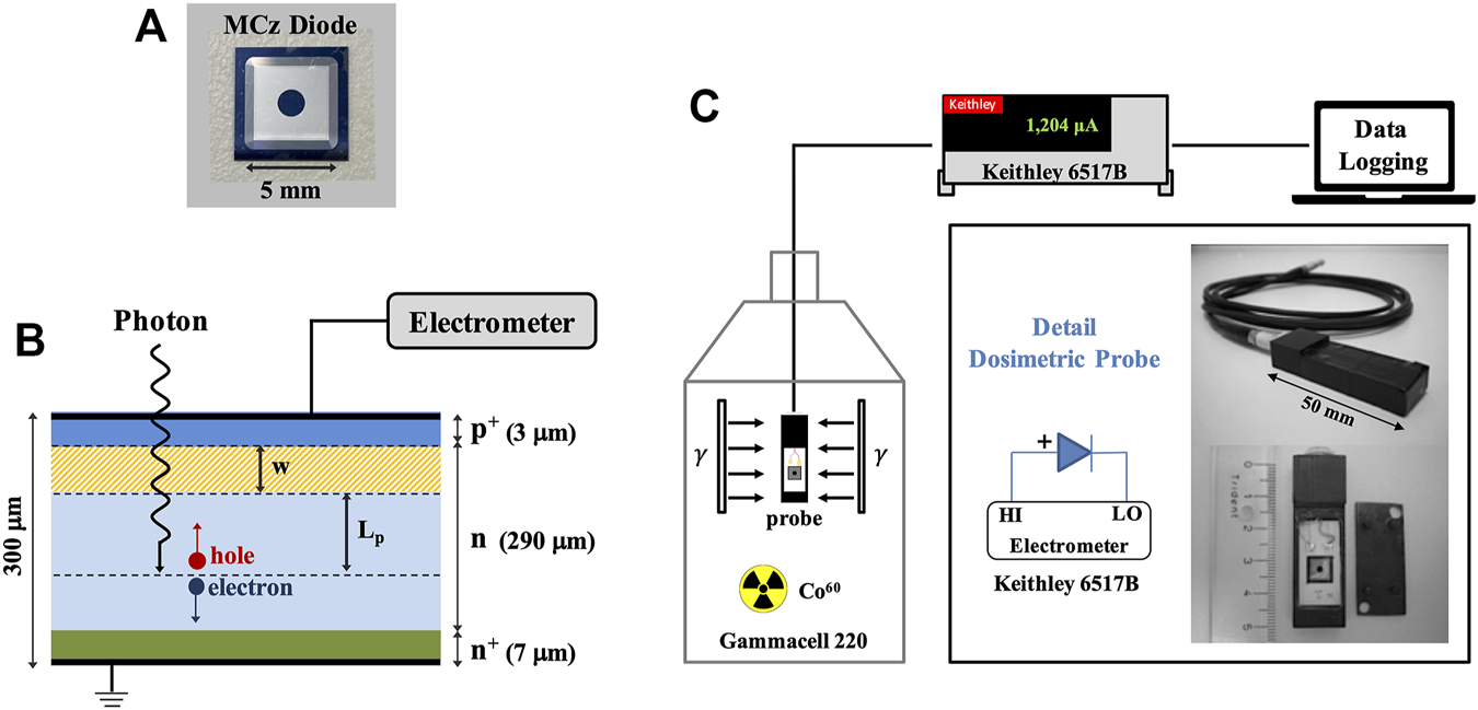
(A) A photograph of the diode; (B) the simplified structure of the diode in the short-circuit mode, and (C) the schematic diagram of the experimental setup.
To enable the diodes to be used as dosimeters, each one was placed in light-tight house-made polymethylmethacrylate (PMMA) probe provided with a miniature coaxial connector with a push-pull self-latching system (Lemo®). A 3 m coaxial cable connects the front p+-layer electrode of the diode to the input of a Keithley 6517B electrometer, configured as an amp-meter with the speed of one power line cycle digital filter on, and range set at 20 µA. The conducting shield of the cable was employed to connect the back n+-layer to the ground of the electrometer while all guard rings were left floating. All induced current measurements were carried out with unbiased diodes (short-circuit mode). Before acquiring each series of data, an offset adjustment procedure (zero correct) was performed to minimize the input bias (offset) current to 5 nA and voltage burden less than 100 μV, leading to an accuracy of (0.1% of reading + 500 pA) for currents up to 20 µA. For analysis, the data acquired by the electrometer were directly sent to a personal computer via the GBIP interface controlled by software developed in LabView.
Irradiations were performed in a small-scale 60Co Gammacell-220 irradiator type I (Atomic Energy of Canada Limited) under a dose rate of 2.3–2.44 kGy/h. Dose rate calibrations were previously obtained through standard reference alanine dosimeters with an expanded uncertainty of 1.7% (k = 2) traceable to the secondary standard laboratory at the International Atomic Energy Agency (IAEA). During the irradiations at a constant dose rate, the basic dosimetric parameter was the prompt induced current signals delivered by the diode. The corresponding charge produced in the diode volume was assessed offline by integrating these current signals. A schematic diagram of the experimental setup is shown in Figure 1C.
The dose-responses of pristine MCz and Fz diodes, i.e., the charge as a function of the absorbed dose, were investigated for doses up to 50 kGy fractionated in incremental steps of 5 kGy by switching on and off the gamma facility system. The same procedure was adopted to check whether the dose-response curve varies with increasing doses, covering 275 kGy. Between each irradiation step, the background current was measured during 120 s to provide the signal-to-noise ratio and monitor the onset of radiation damage effects.
The main dosimetric characteristics regarding the routine dosimeter response, such as repeatability, charge sensitivity, and the degree of dependence on the accumulated dose, were also investigated. The technical procedures adopted were bound to comply with internationally acceptable recommendations for other routine dosimeters, namely alanine (ISO/ASTM 51607, 2013), CTA (ISO/ASTM 51650, 2013), and radiochromic film (ISO/ASTM 51275, 2013), applied here due to the lack of protocols for dosimetry with diodes in radiation processing (ISO/ASTM 51702, 2013).
The repeatability parameter was assessed by the coefficient of variation CV (current standard deviation expressed as a percentage of current average value) (ISO/ASTM 51707, 2015), of current signals delivered by the diode under consecutive irradiation cycles by switching on and off the 60Co facility system. The dose-effect on the repeatability of the current signals, the current sensitivity variation, and the overall performance of the dosimeter was also investigated with radiation-conditioned diodes. The pre-irradiation dose was assessed by continuously irradiating the diode and monitoring the induced current decay to less than 5% variations. The corresponding dose was used to pre-irradiate MCz and Fz diodes to comply with the (ISO/ASTM 51702, 2013) and (ISO/ASTM 52628,2013) recommendations.
The irradiation effect on the dose responses of the diodes was investigated within ranges of 0–50 kGy and 0–275 kGy, following similar procedures to those described above. Moreover, the I-V and C-V measurements of the irradiated diodes were performed to predict somehow their lifespan and reusability as dosimeters.
Finally, some theoretical support for the experimental data was provided by calculations of the minority carrier diffusion lengths as a function of the accumulated dose, considering the induced current measurements, the dose rate, and the thickness of the p+-n-n+ layers.
The overall uncertainty of each performance characteristic was assessed by adding all the components (types A and B) of the standard uncertainties in quadrature. The current uncertainty was obtained from the diode reading (1.1% maximum) and electrometer accuracy (0.2%). The total uncertainty of the charge (3.0–5.3%), assessed via current signal integration, was the quadratic sum of the contributions from the current meter (0.7–1.8%), statistics (2.4–3.6%), time acquisition (1%), and diode positioning (1%). The overall uncertainty on the full depletion voltage (5.2%) was the result of the capacitance (5%) and reverse bias voltage (1%) measurements. The corresponding expanded uncertainty was calculated with a coverage factor k = 2, providing a confidence level of about 95%.
Results and Discussions
Dose-Response of Pristine Diodes
Current signals delivered by pristine diodes during their exposure to doses from 5 kGy up to 50 kGy, at dose rates 2.44 kGy/h (MCz) and 2.36 kGy/h (Fz), are depicted in Figure 2.
FIGURE 2
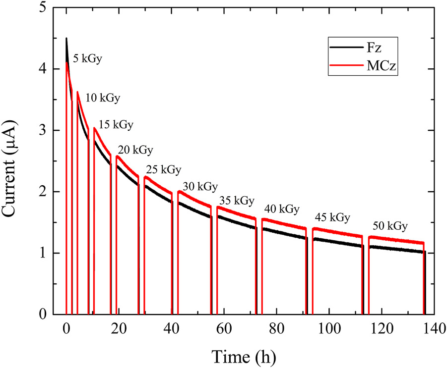
Current signals delivered by pristine MCz and Fz diodes irradiated to doses from 5 kGy up to 50 kGy under dose rates of 2.44 kGy/h (MCz) and 2.36 kGy/h (Fz). Instrumental uncertainties of the current measurements are smaller than the size of the symbols.
All of them exhibit similar patterns revealing a significant drop in their sensitivities with increasing accumulated doses. At the beginning of the irradiation, due to the higher purity level of the Fz diode, its output current is higher than that delivered by the MCz diode. However, a fast drop in the current sensitivity is evidenced even during the first irradiation cycle, being more prominent for the Fz diode. As the only difference between the diodes lies in their oxygen concentration (Table 1), this result indirectly reveals the expected beneficial role of oxygen in reducing the radiation damage effects in silicon. In fact, for 50 kGy, the percentual decrease in the currents related to the maximum values at the beginning of irradiation is found to vary from 68 to 75% for the MCz and Fz diodes, respectively, as shown in Figure 3. It is also important to note that the measurements of the background current carried out between the irradiation cycles (with the radioactive source shielded) remain almost constant (∼15 nA) regardless of the accumulated doses. Such negligible background currents lead to a high current-to-noise ratio (≥102) even at the worst experimental condition, i.e., the maximum accumulated dose and, therefore, the minimum induced current delivered by the unbiased diode.
FIGURE 3
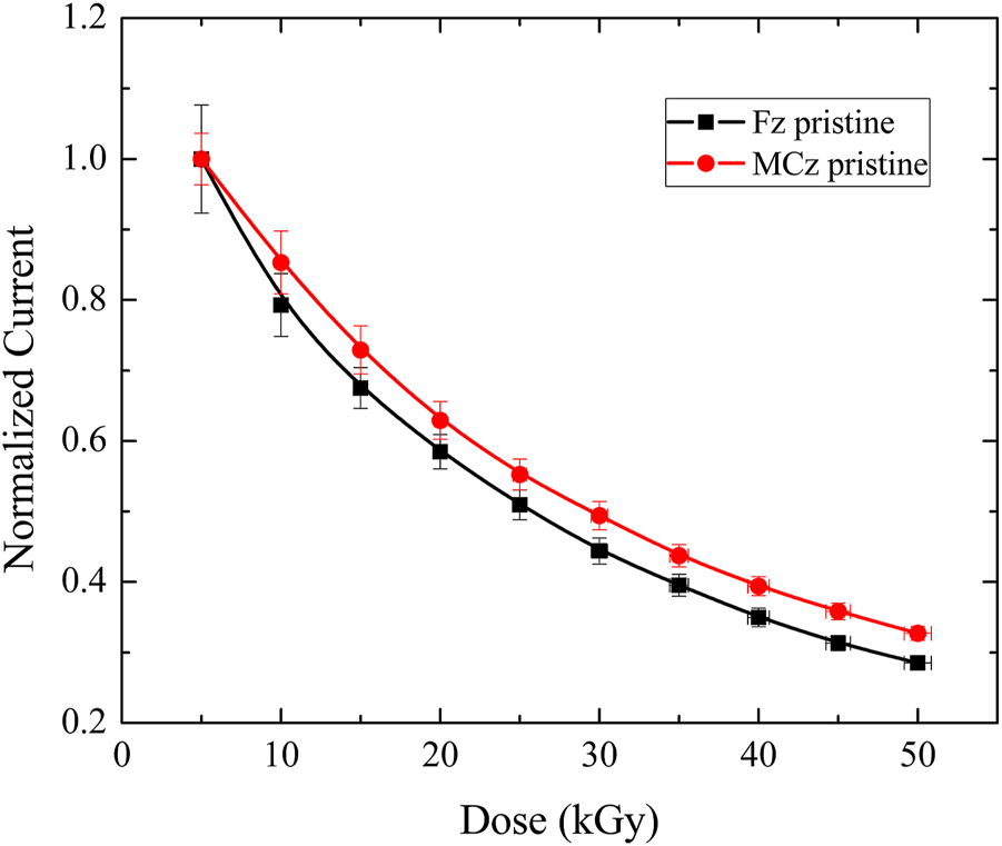
Decrease in the induced currents delivered by Fz and MCz diodes over 50 kGy normalized to the maximum values at the beginning of irradiation.
The dose-response of both diodes covering doses up to 50 kGy is presented in Figure 4, where the nonlinearity between charge and dose is clearly shown. Physically, the visible charge saturation arises from the significant current decay with increasing doses. So, it is impossible to define a single sensitivity parameter for the dosimeter, and a nonlinear function somewhat arbitrary capable of reproducing the dose-response is used instead. In this work, for both diodes, the best fit of the data is found by a fourth-order polynomial function. However, polynomial-based response functions depend on the dose range and cannot be extrapolated outside the dose range over which they are derived. So, as a guide, the response curve of a dosimeter must cover a dose range significantly wider than that intended to be used (ICRU Report 80, 2008).
FIGURE 4
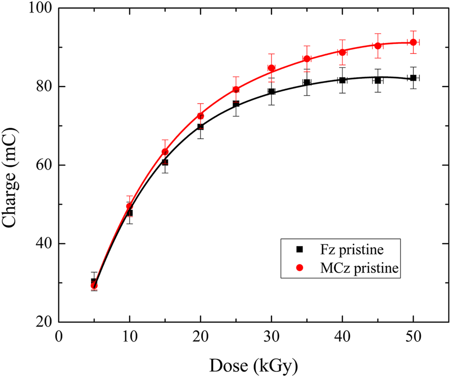
Dose-response curves of pristine Fz and MCz diodes covering the dose range of 50 kGy. A fourth-order polynomial function best fits the data.
For this reason, the dose-responses of both diodes are gathered for doses spanning to 275 kGy, as shown in Figure 5. As expected, the response saturation is visible although smoothed by the greater stability of the current signals at higher absorbed doses. A fourth-order polynomial function best adjusts the data, which validates the ICRU Report 80, 2008 recommendation to determine the degree of the polynomial response of dosimeters independently for each dose range.
FIGURE 5
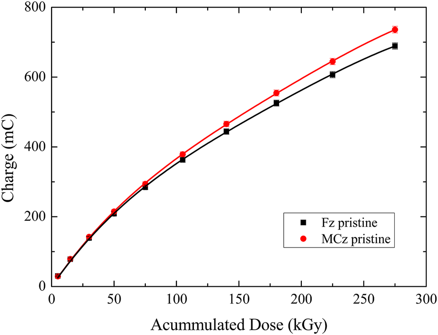
Dose-response curves of pristine Fz and MCz diodes covering the dose range of 275 kGy. The best fit of the data is achieved with a fourth-order polynomial function.
Pre-Irradiation Effect on the Dose-Response
The experimental approach of radiation-conditioning a diode is based on producing so many damage defects in its silicon bulk that, when subjected to radiation, the relative change of the output signals might be neglected. To be used as a routine online dosimeter, the variation in the current signals must be less than 5% to comply with the ISO/ASTM 51702 (2013) and ISO/ASTM 52628 (2013) recommendations. Figure 6 shows the induced current delivered by the MCz diode continuously irradiated to almost 900 kGy under 2.44 kGy dose rate. When the irradiation starts, the current signal is maximum but rapidly diminishes by almost 38% at 25 kGy. However, throughout the irradiation, the relative decrease in the sensitivity slowly tends to saturate. Analyzing the current data in the saturation region and setting the limits of sensitivity variation to less than 5%, the suitable pre-irradiation dose is assessed as 700 kGy. It is important to note that no measurable transient effects were observed throughout all the current readings at null bias. It can be explained by the origin of single event transients (SETs), mostly attributed to the formation of cluster defects by neutrons, charged heavy particles, and energetic ions in the silicon material. However, irradiations in the same medium with 60Co-gamma rays can only lead to single atom displacement and thus to point defects (Moll, 2018). It is expected to be caused by Compton-electrons with a broad distribution of recoil energies for the primary knock-on Si-atoms up to 140 eV, thus below the threshold energy (≅ 5 keV) for cluster generation (Pintilie et al., 2009). Therefore, it is unlikely that 60Co-gamma rays create clusters directly and give rise to measurable single transient effects.
FIGURE 6
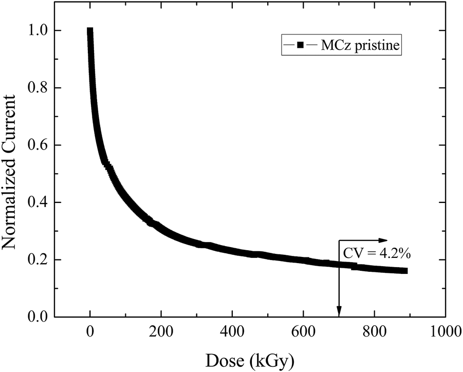
Decrease in the induced currents delivered by a pristine MCz diode over 900 kGy related to the maximum values at the beginning of irradiation. For doses higher than 700 kGy, the coefficient of variation (CV) of the current signals is 4.2%.
The current signals delivered by both diodes preirradiated to 700 kGy and exposed to different absorbed doses up to 50 kGy at 2.39 kGy/h (MCz) and 2.33 kGy/h (Fz), are shown in Figure 7.
FIGURE 7
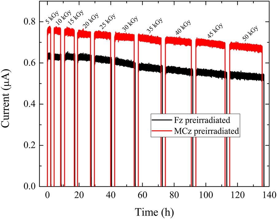
Current signals delivered by the MCz and Fz diodes preirradiated to 700 kGy. Doses span from 5 to 50 kGy in incremental steps of 5 kGy under dose rates of 2.39 kGy/h (MCz) and 2.33 kGy/h (Fz). Instrumental uncertainties in the current measurements are smaller than the size of the symbols.
Despite a significant decrease in amplitudes, the signals are stabler than those recorded with pristine diodes (Figure 2). The beneficial influence of the accumulated dose on the repeatability of the current signals is assured by the coefficient of variations (CV) being less than 3% (MCz) and 4% (Fz), which fully adhere to ISO/ASTM 51702 (2013), ISO/ASTM 52628 (2013) protocols. Furthermore, analysis of the induced current values also reveals that the MCz diode remains slightly more sensitive than the Fz one.
The higher current sensitivity of the MCz diode manifests itself in its higher charge sensitivity, as shown in Figure 8, where the charge generated in the volume of each diode is plotted as a function of dose covering up to 50 kGy. Moreover, due to the better stability of the current signals from both preirradiated diodes, the data is best fitted by a second-order polynomial function. Similar results obtained with both diodes irradiated to 275 kGy are exhibited in Figure 9.
FIGURE 8
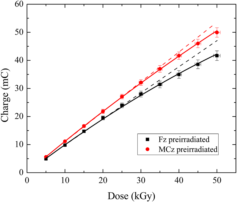
Dose-response curves of the Fz and MCz diodes preirradiated to 700 kGy covering the dose range of 50 kGy. The best fit to the data is achieved with a second-order polynomial function. For comparison, the dashed lines show the departure from linearity in the high-dose region.
FIGURE 9
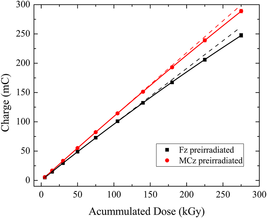
Dose-response curves of the preirradiated Fz and MCz diodes covering the dose range of 275 kGy. A second-order polynomial function best fits the data. For comparison, the dashed lines show the departure from linearity in the high-dose region.
The data sets in Figures 8, 9 show reasonable linearity between charge and dose (dashed lines), mainly for the MCz diode. It enables the charge sensitivities of both diodes to be assessed through the slope of each linear dose-response and the corresponding dose linearity parameters. For comparison purposes, all relevant dosimetric parameters gathered with MCz and Fz diodes are shown in Table 2. An analysis of the data on charge sensitivities, dose linearity, and repeatability parameters reassures the better dosimetric performance of the MCz diode. It is worth noting that the dose linearity of the preirradiated MCz diode adheres to the AAPM Report 87-TG62, 2005 that recommends the variation of this parameter to be in the range 0.98–1.02.
TABLE 2
| Diode | Condition | Best fit (polynomial) | SQ (µC/Gy) | Dose linearity (0.98–1.02)a | CV (%) |
|---|---|---|---|---|---|
| MCz | pristine | 4th-order | ------ | ------ | 5.3 |
| MCz | preirrad | 2nd-order | 1.062 ± 0.004 | 0.98 | 3.1 |
| Fz | pristine | 4th-order | ------ | ------ | 7.7 |
| Fz | preirrad | 2nd-order | 0.915 ± 0.006 | 0.96 | 4.2 |
Relevant dosimetric parameters of MCz and Fz diodes.
accepted interval according to AAPM, Report 87-TG62 (2005).
Electrical Characterization of the Irradiated Diodes
It is well-known that radiation-induced damage on silicon diodes manifests itself in increasing both the dark currents and the full depletion (Vfd) voltage when they are reversely biased. Therefore, both electrical features can be indirectly used to monitor the degree of damage induced on MCz and Fz diodes irradiated up to 975 kGy and somehow predict their dose lifespans as dosimeters.
Measurements of dark currents (I) as a function of the reverse voltage (V) have been carried out shortly after the end of each step of irradiation up to 975 kGy. The data gathered with the MCz diode are shown in Figure 10, revealing similar shapes of all I-V curves characterized by the increase of the dark current with reverse bias and accumulated dose. For example, the dark current varies from 0.03 nA (0 Gy) to 0.63 nA (975 kGy) at 0 V and from 35.67 nA (0 Gy) to 747.41 nA (975 kGy) at 400 V. It is worth noting that at 0 V, the dark current is about three orders of magnitude lower than the radiation-induced currents, even when the diode is heavily irradiated to 975 kGy.
FIGURE 10
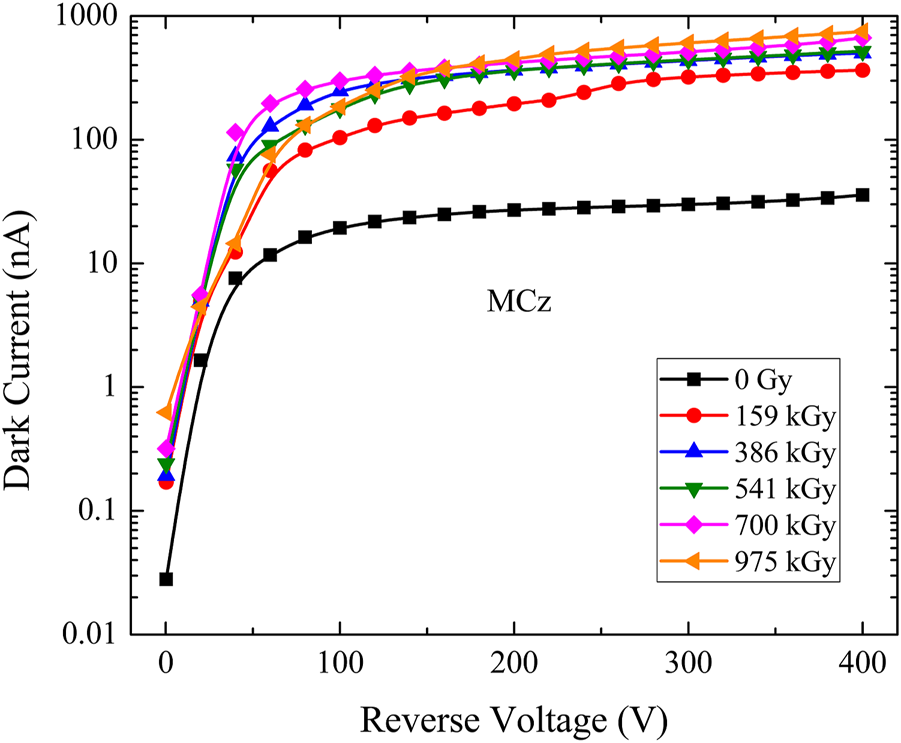
Dark current as a function of the reverse voltage of one pristine MCz diode (0 Gy) and after irradiation up to 975 kGy in incremental steps of almost 150 kGy.
These results, obtained with MCz and Fz diodes, confirm the double advantages of the lowest generation of dark currents and the smallest difference between the dark currents after and before radiation damage when using the diode without externally applied voltage. Capacitance measurements performed as a function of the reverse voltage applied to the MCz diode subjected to different doses are shown in Figure 11.
FIGURE 11
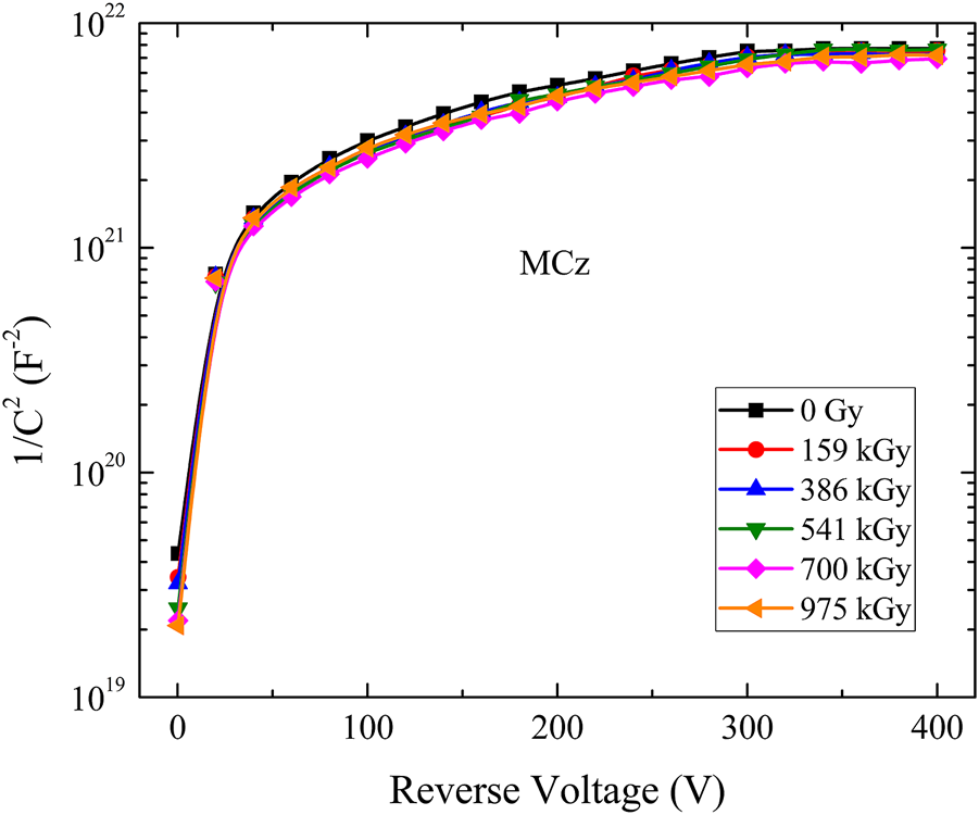
Capacitance measurements, plotted as 1/C2 versus the reverse voltage applied to a pristine MCz diode (0 Gy) and after irradiation up to 975 kGy in incremental steps of almost 150 kGy.
The data plotted as 1/C2 × V enables the full depletion voltage (Vfd) to be assessed as corresponding to the beginning of the plateau. For the MCz, with a 300 µm thick substrate, the plateau starts at about 310 V. For comparison, in the Fz diode with the same substrate thickness, the full depletion occurs at about 210–225 V. The doping concentration and resistivity can be calculated from the well-known formula (Lutz, 2007) of the full depletion voltage:where e is the elementary charge, Neff is the effective doping concentration, d is the thickness of the substrate, ε0 is the dielectric constant of the vacuum, and εSi is the dielectric constant of silicon. The values of Vfd and Neff at different accumulated absorbed doses in the two diodes, depicted in Figure 12, show a good agreement with those measured in MCz and Fz silicon substrates (dashed lines). It thus reveals that the radiation damage induced in both diodes by doses up to almost 1 MGy is not enough to change these parameters. These results are corroborated by the data on radiation damage effects available in the literature addressing the high radiation hardness of these diodes for gamma-rays, neutrons, and charged particles subject to much higher doses (Moll, 2018). Furthermore, as the diode endures to accumulated doses of 1 MGy, including the radiation conditioning with 700 kGy, its minimum dose lifespan can be inferred as 300 kGy, which in itself is quite high when compared to the well-established passive dosimeters in radiation processing dosimetry. It means that the device can be reused at least ten times for monitoring processes encompassing doses of 30 kGy each before needing recalibrations. However, the real dose lifespan, assessed through the maximum dose that the diode can withstand still complying with the (ISO/ASTM 51702,2013) and (ISO/ASTM 52628,2013) recommendations for response stability better than 8% (k = 2), is not yet reached. Investigations in this direction are underway.
FIGURE 12
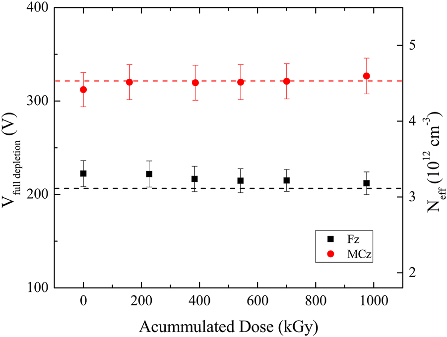
Full depletion voltages and effective doping concentrations (right axis) of pristine MCz and Fz diodes and irradiated up to 975 kGy in incremental steps of almost 150 kGy. The dashed lines indicate the values obtained for the MCz and Fz silicon substrates.
It is worth noting that such a high-dose lifespan, essential for process monitoring with electronic dosimeters, has only been achieved thanks to the outstanding radiation hardness of the MCz diode developed by defect-engineering techniques. To the best of our knowledge, there is no similar characterization of electronic dosimeters for absorbed doses up to almost 300 kGy in radiation processing applications. In addition to its high-dose lifespan, the MCz diode, as a dosimeter, bears advantages of easy reading and handling, suitable repeatability, stable response function, and low cost. Indeed, at high dose rates, the current readings can be performed by conventional electrometers, whereas the MCz diodes are produced at a very affordable price (one 6″ Si wafer results in approximately 200 diodes, and typically five wafers batches are processed, i.e., the unit price is quite low). Furthermore, its employment is quite simple compared to other passive dosimeters with an operational dose range higher than 100 kGy. For example, Alanine-EPR (10 Gy–150 kGy) (ISO/ASTM 51607, 2013), cellulose triacetate (CTA) (10–300 kGy) (ISO/ASTM 51650, 2013), and polymethyl methacrylate (PMMA) Radix-W (1–150 kGy) (ISO/ASTM 51276, 2019), are all single-use due to the saturation effects associated with radiation damage.
The readout of the alanine dosimeter is based on detecting free radicals by electron-paramagnetic resonance (EPR) spectroscopy. Both the radiation chemistry and the EPR spectrum of irradiated alanine are complex; however, alanine-EPR is a precise and accurate dosimetric system for transfer dosimetry in industrial radiation processing by primary and secondary standards dosimetry laboratories. Alanine is also a reference standard often used to calibrate routine dosimeters. However, the EPR system is neither cheap nor simple to operate, requiring technical skills from the operator. Despite that, the availability of compact EPR spectrometers has enabled alanine to be used as routine dosimeter.
The polymer-based CTA and PMMA Radix-W film dosimeters, whose performances are not as good as alanine, have been largely used for day-to-day measurements in a radiation processing facility mainly due to their low cost and ease of use. The dosimetry principle is based on their coloration change due to radiation-induced chemical reactions. The dosimetric parameter, the increment of absorbance per nominal thickness at an appropriate wavelength, is readout by optical spectrometry regardless of the type of dosimeter. Nevertheless, the response of polymer-based dosimeters is affected by complex interactions between the influence quantities (e.g., irradiation temperature, pre-and post-irradiation storage conditions, relative humidity, exposure to light both before and after irradiation), preventing the corresponding correction factors to be straightforwardly applicable. For this reason, careful experimental design is needed to calibrate the dosimeter under the conditions of the final use, as post-calibration corrections are generally not possible.
Summing up, the wide variety of processes with high absorbed doses and extreme environmental conditions pose particular dosimetry challenges. Consequently, different and complementary dosimetry systems are needed, tailored to specific radiation processing applications. Developing the online MCz diode-based dosimeter system focused on the routine monitoring process is a part of this context.
Calculations
The results of this work, regarding the current response of unbiased diodes continuously irradiated, have shown a sensitivity drop with increasing absorbed doses. Regardless of the diode type, this current sensitivity decay is fast at the beginning of irradiation, tending to stabilize with the accumulation of absorbed doses. This effect is physically attributed to the decrease in the minority carrier diffusion lengths due to the production of generation-recombination centers in the silicon bulk by impinging gamma radiation. Considering that only the excess minority carriers, generated throughout the crystal over a distance of their diffusion lengths, can be swept by the built-in voltage in the depletion layer, the decrease in the diffusion length might reduce the sensitive detection volume. So, the sensitivity and diffusion lengths decay trends are expected to be somewhat similar within the absorbed dose range herein investigated. In an attempt to add some numerical support to this analysis, calculations of the radiation-induced current in a p-n junction taking into account the electron-hole injection rate, the junction area, the thicknesses of the p-n layers, and the corresponding minority carrier diffusion lengths are performed. The expression used was deduced assuming an ordinary p-n junction reversely biased for an infinitely thick wafer (Lutz, 2007), which with appropriate changes for the short-circuit regime (Osvay and Tárczy, 1975; Gylar and Petr, 1985), without externally applied voltage, is given by:where e is the elementary charge; Ln is the diffusion lengths of electrons in the p layer, Lp is the diffusion lengths of holes in the n layer; dn and dp are the thicknesses of the n and p layers, respectively; g is the number of excess charge carriers generated by the radiation per unit volume and unity time; S is the area of the p-n junction. These parameters are known under the irradiation condition for both diodes, except for the Ln and Lp diffusion lengths. The latter quantities can be assessed from the minority carrier recombination lifetime measured earlier by the Microwave Photoconductivity Decay (µPCD) method (Härkönen et al., 2003). The µPCD measurement returns a parameter called effective lifetime, which depends, in a complex way, from the effects of recombination processes both in the bulk and the sample surface (Cuevas and McDonalds, 2004). The effective lifetime values are higher than 250 µs (MCz) and 650 µs (Fz), leading to Ln (935 µm) and Lp (557 µm) for the MCz material, and Ln (1,510 µm) and Lp (898 µm) for the Fz one. These values enable induced current calculations only for pristine diodes since the diffusion lengths diminish with increasing accumulated doses. The current calculations for Fz and MCz diodes are almost 10% lower than the corresponding average induced current readings. Three possible oversimplifications might explain this difference: i) using a single lifetime constant for electrons and holes to calculate the corresponding diffusion lengths; ii) the expression was deduced for ordinary p-n junctions neglecting the depleted zone layer thickness of unbiased diodes and, therefore, the contribution of the electron-hole pairs generated there; iii) the MCz and Fz diodes are built of an abrupt junction of a shallow highly doped (NA = 1018 cm−3) p-region on a thick low-doped (ND = 1012 cm−3) n-bulk material, which warrants to reexamine the boundary conditions that have led to the expression herein used. Although interesting, this issue is not within the scope of this work, but studies addressing it are underway.
So, to roughly predict the variation in the minority carrier diffusion length as a function of the dose, a semiempirical approach is adopted, based on the following assumptions: i) the contribution to the current of the second term in Eq. 2 (electron diffusion in the p+ layer) is negligible, ii) the average induced current in each step of irradiation is mostly due to the hole diffusion (n-substrate) toward the depletion zone, iii) at 0 V the thickness of the depletion zone can be neglected. If these assumptions hold, the hole diffusion length can be calculated considering the n-layer thickness, the junction area, the generation rate of the electron-hole pairs per unit of volume, and the average induced current in each step of irradiation. As a matter of fact, i) and ii) ensure that the value of Lp is only weekly correlated with the assumed value of Ln. On the contrary, any uncertainty in g or S or the limitation introduced by iii) strongly affects Lp because of the exponentials appearing in Eq. 2. A correction for the difference between the energy deposited per unit mass in water (dose-rate calibration) and silicon has also been applied. The normalized Lp results as a function of the dose are shown in Figure 13 for both pristine and preirradiated diodes. It is worth noting that the diffusion length drops with increasing doses for pristine diodes, and the known stabilizing effect of pre-irradiation on diffusion length is clearly visible. Furthermore, regardless of the accumulated dose, the diffusion length in the MCz material is slightly greater than in the Fz one.
FIGURE 13
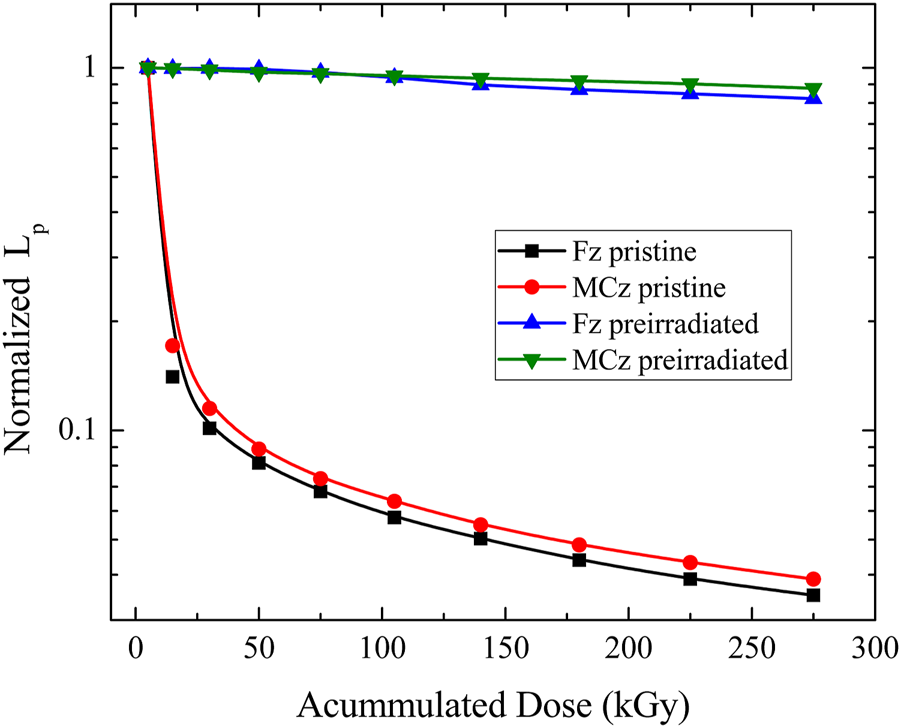
Normalized variation in hole diffusion lengths as a function of accumulated doses for pristine and preirradiated MCz and Fz diodes.
Conclusion
In this work, the dosimetric response of two types of silicon diodes produced with distinct engineering technologies, Magnetic Czochralski (MCz) and standard Float Zone (Fz), have been investigated, aiming their application to gamma radiation processing dosimetry. Both diodes, operating in the short-circuit mode and under industrial irradiation conditions at 2.33–2.44 kGy/h, deliver current signals whose intensities drop with increasing accumulated doses. Mitigation of this decay has been accomplished by pre-irradiating the devices to 700 kGy. The dose responses of both diodes, assessed offline through the integration of the current signals, are best represented by polynomial functions. The relevant dosimetric parameters as response stability, charge sensitivity, repeatability of current signals (<5%), and radiation hardness reveal the better performance of the MCz diode. Furthermore, the whole dataset fully complies with the international standard protocols for routine dosimeters in radiation processing dosimetry.
Regarding radiation damage, which in unbiased diodes manifests primarily in the decay of current sensitivity, the results also showed the greater tolerance of the MCz diode. Since the essential difference between the diodes is the oxygen concentration, these results corroborate the beneficial role of oxygen on the radiation damage effects in silicon devices. Furthermore, the decrease in current with accumulated doses is mainly associated with radiation-induced point defects in the crystal bulk with energy levels within the bandgap. Such defects act as recombination centers, reducing the minority carrier lifetime and creating a gradual sensitivity decay. In this regard, some numerical support is given by roughly calculating the variation trend in hole diffusion lengths, taking into account the average induced current data as a function of accumulated doses.
Based on the latter considerations and the excellent dosimetric characteristics, large availability, and better cost-effectiveness of MCz diodes, it is possible to endorse their potential use as online routine dosimeters in radiation processing applications. However, for the sake of characterization completeness, the data reproducibility, the operational dose lifespan, and the effect of the irradiation conditions (e.g., temperature, relative humidity, dose fractionating) remain to be investigated. Works in this direction are currently in progress.
Statements
Data availability statement
The raw data supporting the conclusions of this article will be made available by the authors, without undue reservation.
Author contributions
CB contributed with conceptualization, methodology, formal analysis, writing—original draft, funding, supervision. FC performed investigation, formal analysis, visualization, resources, review. JG contributed with methodology, investigation, formal analysis, resources, visualization, review and editing. KP performed investigation and resources. AM contributed with calculations and review. ET contributed with the investigation, resources, and review. JH contributed with the investigation, resources, and review.
Funding
This work was partially supported by Energy and Nuclear Researche Institute (under DPDE Edital 2017).
Acknowledgments
The authors are grateful to Eng° Elisabeth S. R. Somessari from Gammacell and Panoramic irradiators staff (IPEN-CNEN/SP) for her indispensable help during the irradiations. The authors also thank R. C. Teixeira (Electronic Packaging staff) and N. Carvalho (Electronic Products Analysis and Qualification Research Group), both from Centro de Tecnologia da Informação Renato Archer (CTI-Renato Archer, Campinas/SP), for useful discussions and the measurements of I-V and C-V curves. FC acknowledges a fellowship by FAPESP, under Contract 05/00258-1. KP and AM acknowledge a fellowship and support by Brazilian National Council for Scientific and Technological Development (CNPq), contracts 133904/2008-3 and 311915/2020-5, respectively.
Conflict of interest
The authors declare that the research was conducted in the absence of any commercial or financial relationships that could be construed as a potential conflict of interest.
Publisher’s note
All claims expressed in this article are solely those of the authors and do not necessarily represent those of their affiliated organizations, or those of the publisher, the editors and the reviewers. Any product that may be evaluated in this article, or claim that may be made by its manufacturer, is not guaranteed or endorsed by the publisher.
References
1
AAPM Report 87-TG62 (2005). Diode in Vivo Dosimetry for Patients Receiving External Beam Radiation Therapy. ISBN 1-888.340-50-9.
2
Andjelkovic M. Ristic G. (2013). Feasibility Study of a Current Mode Gamma Radiation Dosimeter Based on a Commercial PIN Photodiode and a Custom Made Auto-Ranging Electrometer. Nucl. Tech. Rad Prot.28, 73–83. 10.2298/NTRP1301073A
3
Cuevas A. Macdonald D. (2004). Measuring and Interpreting the Lifetime of Silicon Wafers. Solar Energy76, 255–262. 10.1016/j.solener.2003.07.0310.1016/j.solener.2003.07.033
4
Dixon R. L. Ekstrand K. E. (1982). Silicon Diode Dosimetry. Int. J. Appl. Radiat. Isotopes33, 1171–1176. 10.1016/0020-708X(82)90242-3
5
Fretwurst E. Hönniger F. Kramberger G. Lindström G. Pintilie I. Röder R. (2007). Radiation Damage Studies on MCz and Standard and Oxygen Enriched Epitaxial Silicon Devices. Nucl. Instr. Methods Phys. Res. Section A: Acc. Spectrometers, Detectors Associated Equipment583, 58–63. 10.1016/j.nima.2007.08.194
6
Fretwurst E. Lindström G. Stahl J. Pintilie I. Li Z. Kierstead J. et al (2003). Bulk Damage Effects in Standard and Oxygen-Enriched Silicon Detectors Induced by 60Co-Gamma Radiation. Nucl. Instr. Methods Phys. Res. Section A: Acc. Spectrometers, Detectors Associated Equipment514, 1–8. 10.1016/j.nima.2003.08.077
7
Gilar O. Petr I. (1985). Silicon Photodiode as a Detector of Exposure Rate. Nucl. Instr. Methods Phys. Res. Section A: Acc. Spectrometers, Detectors Associated Equipment234, 566–572. 10.1016/0168-9002(85)91009-5
8
Goncalves J. A. C. Mangiarotti A. Bueno C. C. (2020). Current Response Stability of a Commercial PIN Photodiode for Low Dose Radiation Processing Applications. Radiat. Phys. Chem.167, 108276–108279. 10.1016/j.radphyschem.2019.04.026
9
Gonçalves J. A. C. Mangiarotti A. Asfora V. K. Khoury H. J. Bueno C. C. (2021). The Response of Low-Cost Photodiodes for Dosimetry in Electron Beam Processing. Radiat. Phys. Chem.181, 109335–109342. 10.1016/j.radphyschem.2020.109335
10
Härkönen J. (2013). Development of Radiation Hard Particle Detectors Made of Czochralski Grown Silicon. Acta Phys. Pol. A.124, 372–376. 10.12693/APhysPolA.124.372
11
Härkönen J. Tuominen E. Lassila-Perini K. Palokangas M. Yli-koski M. Ovchinnikov V. et al (2002). Processing and Recombination Lifetime Characterization of Silicon Microstrip Detectors. Nucl. Instrum. Methods A.485, 159. 10.1016/S0168-9002(02)00548-X
12
Härkönen J. Tuominen E. Tuovinen E. Mehtälä P. Lassila-Perini K. Ovchinnikov V. et al (2003). Processing of Microstrip Detectors on Czochralski Grown High Resistivity Silicon Substrates. Nucl. Instr. Methods Phys. Res. Section A: Acc. Spectrometers, Detectors Associated Equipment514, 173–179. 10.1016/j.nima.2003.08.102
13
Härkönen J. Tuovinen E. Luukka P. Tuominen E. Lassila-Perini K. Nysten J. et al (2004). Particle Detectors Made of High Resistivity Czochralski Grown Silicon. Phys. Scr.T114, 88–90. 10.1088/0031-8949/2004/T114/021
14
Härkönen J. Tuovinen E. Luukka P. Tuominen E. Li Z. Ivanov A. et al (2005). Particle Detectors Made of High-Resistivity Czochralski Silicon. Nucl. Instr. Methods Phys. Res. Section A: Acc. Spectrometers, Detectors Associated Equipment541, 202–207. 10.1016/j.nima.2005.01.057
15
Hönniger F. Fretwurst E. Lindström G. Kramberger G. Pintilie I. Röder R. (2007). DLTS Measurements of Radiation Induced Defects in Epitaxial and MCz Silicon Detectors. Nucl. Instr. Methods Phys. Res. Section A: Acc. Spectrometers, Detectors Associated Equipment583, 104–108. 10.1016/j.nima.2007.08.202
16
ICRU Report 80 (2008). International Commission on Radiation Units and Measurements, Dosimetry Systems for Use in Radiation Processing, ICRU Report 80 (International Commission on Radiation Units and Measurements. 10.1093/jicru/ndn031
17
ISO/ASTM 51275 (2013). Practice for Use of a Radiochromic Film Dosimetry System. ISO.Geneva, Switzerland10.1520/ISOASTM51275-13
18
ISO/ASTM 51276 (2019). Practice for Use of a Polymethylmethacrylate Dosimetry System. ISOGeneva, Switzerland .
19
ISO/ASTM 51607. (2013). Practice for Use of the Alanine-EPR Dosimetry System. ISOGeneva, Switzerland10.1520/ISOASTM51607-13
20
ISO/ASTM 51649 (2015). Practice for Dosimetry in an Electron Beam Facility for Radiation Processing at Energies between 300 keV and 25 MeV. 3rd ed. ISO.Geneva, Switzerland10.1520/ISOASTM51649-15
21
ISO/ASTM 51650 (2013). Practice for Use of a Cellulose Triacetate Dosimetry System. ISO.Geneva, Switzerland10.1520/ISOASTM51650-13
22
ISO/ASTM 51702 (2013). Standard Practice for Dosimetry in a Gamma Facility for Radiation Processing. 3rd ed.ISO.Geneva, Switzerland10.1520/ISOASTM51702-13
23
ISO/ASTM 51707 (2015). Standard Guide for Estimation of Measurement Uncertainty in Dosimetry for Radiation Processing. 3rd ed.ISO.Geneva, Switzerland10.1520/ISOASTM51707-15
24
ISO/ASTM 52628 (2013). Standard Practice for Dosimetry in Radiation Processing. 1st ed.ISO.Geneva, Switzerland. 10.1520/ISOASTM52628-13
25
Lindström G. Moll M. Fretwurst E. (1999). Radiation Hardness of Silicon Detectors - a challenge from High-Energy Physics. Nucl. Instr. Methods Phys. Res. Section A: Acc. Spectrometers, Detectors Associated Equipment426, 1–15. 10.1016/S0168-9002(98)01462-4
26
Lindström G. (2001). Radiation Hard Silicon Detectors Developments by the RD48 (ROSE) Collaboration. Nucl.Instr.Methods A466, 308. 10.1016/S0168-9002(01)00560-5
27
Lutz G. (2007). Semiconductor Radiation Detectors. Springer-Verlag Berlin Heidelberg, second printing. 10.1007/978-3-540-71679-2
28
McLaughlin W. L. Desrosiers M. F. (1995). Dosimetry Systems for Radiation Processing. Radiat. Phys. Chem.46 (4-6), 1163–1174. 10.1016/0969-806X(95)00349-3
29
Menichelli D. Scaringella M. Miglio S. Bruzzi M. Pintilie I. Fretwurst E. (2006). Shallow Energy Levels Induced by γ Rays in Standard and Oxygenated Floating Zone Silicon. Appl. Phys. A.84, 449–453. 10.1007/s00339-006-3640-y
30
Möhlmann J. H. F. (19811981). “The Use of Solar Cells for Continuous Recording of Absorbed Dose in the Product during Radiation Sterilization,” in Biomedical Dosimetry, Proceedings of Symposium (Vienna: IAEA Publication STI/PUB/567), 563.
31
Moll M. (2018). Displacement Damage in Silicon Detectors for High Energy Physics. IEEE Trans. Nucl. Sci.65 (8), 1561–1582. 10.1109/TNS.2018.2819506
32
Muller A. C. (1970a). “The "n" on "p" Solar-Cell Dose-Rate Meter,” in Manual on Radiation Dosimetry. Editors HolmN. W.BerryR. J. (New York, 423.
33
Muller A. C. (1970b). “The "p" on "n" Solar-Cell Integrating Dosimeter,” in Manual on Radiation Dosimetry. Editors HolmN. W.BerryR. J. (New York, 429.
34
Osvay M. Stenger V. Földiak G. (19751974). “Silicon Detectors for Measurement of High Exposure Rate Gamma Rays,” in Biomedical Dosimetry, Proceedings of Symposium (Vienna: IAEA Publication STI/PUB/401), 623.
35
Osvay M. Tárczy K. (1975). Measurement of γ-dose Rates by N- and P-type Semiconductor Detectors. Phys. Stat. Sol. (A)27, 285–290. 10.1002/pssa.2210270134
36
Pintilie I. Lindstroem G. Junkes A. Fretwurst E. (2009). Radiation-induced point- and Cluster-Related Defects with strong Impact on Damage Properties of Silicon Detectors. Nucl. Instr. Methods Phys. Res. Section A: Acc. Spectrometers, Detectors Associated Equipment611, 52–68. 10.1016/j.nima.2009.09.065
37
Väyrynen S. Härkönen J. Tuominen E. Kassamov I. Tuovinen E. Räisänen J. (2011). The Effect of an Electrical Field on the Radiation Tolerance of Float Zone and Magnetic Czochralski Silicon Particle Detectors. Nucl. Instrum. Methods A.637, 95. 10.106/j.nima.2011.02.033
Summary
Keywords
Si diodes, radiation processing, high-dose dosimetry, gamma dosimetry, rad-hard Si diodes, MCz diode
Citation
Bueno CC, Camargo F, Gonçalves JAC, Pascoalino K, Mangiarotti A, Tuominen E and Härkönen J (2022) Performance Characterization of Dosimeters Based on Radiation-Hard Silicon Diodes in Gamma Radiation Processing. Front. Sens. 3:770482. doi: 10.3389/fsens.2022.770482
Received
03 September 2021
Accepted
10 January 2022
Published
31 January 2022
Volume
3 - 2022
Edited by
Patrice Megret, University of Mons, Belgium
Reviewed by
Santosh Kumar, Liaocheng University, China
Alexandre Quenon, University of Mons, Belgium
Updates
Copyright
© 2022 Bueno, Camargo, Gonçalves, Pascoalino, Mangiarotti, Tuominen and Härkönen.
This is an open-access article distributed under the terms of the Creative Commons Attribution License (CC BY). The use, distribution or reproduction in other forums is permitted, provided the original author(s) and the copyright owner(s) are credited and that the original publication in this journal is cited, in accordance with accepted academic practice. No use, distribution or reproduction is permitted which does not comply with these terms.
*Correspondence: C. C. Bueno, ccbueno@ipen.br
Deceased
This article was submitted to Physical Sensors, a section of the journal Frontiers in Sensors
Disclaimer
All claims expressed in this article are solely those of the authors and do not necessarily represent those of their affiliated organizations, or those of the publisher, the editors and the reviewers. Any product that may be evaluated in this article or claim that may be made by its manufacturer is not guaranteed or endorsed by the publisher.