 Chumki Das
 Kaushik Mazumdar*
- Department of Electronics Engineering, IIT (ISM) Dhanbad, Dhanbad, India
In this paper, we investigated the logic and RF performance of nanostructure N-polar AlGaN/GaN high-electron mobility transistors (HEMTs) with and without GaN cap layer. It’s found that devices without the GaN cap layer exhibit superior performance, the maximum drain current density of 0.99 mA/μm at VGS = 2 V and a corresponding on-state resistance (Ron) of 0.88 Ω·mm. The GaN HEMT without GaN cap layer leads to a peak transconductance of 0.75 S/mm at VDS = 3 V. Varying the drain doping concentration significantly affects both the current density and transconductance. At a doping concentration (ND) of 1022 cm−3, the device without GaN cap layer achieves a maximum current density of 0.98 mA/μm at VDS = 1 V, and the maximum cut-off frequency (fT) of 183.8 GHz at VDS = 3 V. These findings highlight the potential of N-polar AlGaN/GaN HEMTs without the GaN cap layer for high-power, high-frequency, and micro- and nano-electromechanical system (M/NEMS) sensors applications.
1 Introduction
AlGaN/GaN HEMTs are highly effective for high-power, and high-frequency applications. This effectiveness arises from their outstanding material properties, characterized by a wide energy bandgap, saturation velocity, high breakdown voltage, and a substantial density of two-dimensional electron gas (2DEG) at the AlGaN/GaN heterointerface [1–4]. The strong mechanical stability of epitaxial films enables the III-N materials HEMTs for micro-electromechanical system (MEMS) sensors and oscillators [5–7]. The size of nano electromechanical device can be scaled [8]. The wurtzite crystal structure of GaN causes polarization in the c-direction. Thus, the orientation of the substrate can result in epitaxial structures with either N-polarity or Ga-polarity. Currently, most commercial AlGaN/GaN HEMTs utilize Ga-polar orientation because it’s simplifying epitaxial growth process and more mature processing techniques [9]. However, the reversed polarization found in N-polar epitaxial structures that may offer advantages for N-polar HEMTs. In N-polar HEMTs, unlike Ga-polar HEMTs, the barrier layer is situated below the channel. This arrangement enables the gate-to-channel distance to be scaled further without reducing the density of the 2DEG [10, 11]. N-polar GaN HEMTs exhibit superior performance as higher-frequency and higher-power amplifiers than their Ga-polar [12]. Additionally, due to its position beneath the channel, the barrier layer acts as a built-in back barrier, enhancing the device’s pinch-off performance [13]. Furthermore, in N-polar GaN, a thick GaN-cap layer can be applied. The N-polar HEMT epi structure featuring a GaN cap is often termed a “deep recess HEMT” due to its requirement for recess etching to position the gate in closer proximity to the channel [14, 15]. The GaN cap layer reduces the vertical electric field in the GaN channel, leading to an increase in 2DEG charge density and improved mobility [16]. Additionally, the GaN cap helps control dispersion by shifting surface states away from the channel and increasing the threshold voltage (VTH) in the access regions [17]. This voltage shifts results from the higher sheet charge density induced by the polarization effects of the GaN layer.
Despite these benefits, deep recess N-polar HEMTs face certain challenges. The interface between the gate and GaN, particularly at the trench sidewalls, can lead to higher leakage currents due to damage caused by dry etching [18]. Additionally, the deep recess structure introduces fringing capacitance from the gate recess through the GaN cap layer, limiting the device gain [19] which can degrade RF performance [20]. Furthermore, incorporate of a GaN cap layer in N-polar HEMTs creates challenges such as increased surface roughness, complexities in managing polarity reversal during growth, and potential interfacial strain and defects [21, 22]. Removing the GaN cap layer in N-polar HEMTs can offer several significant advantages, primarily related to improved device performance and fabrication simplicity. Without the GaN cap layer, the overall surface roughness of the device can be reduced, leading to better electron mobility and enhanced high-power performance [23]. The absence of the cap layer also simplifies the growth process, reducing the complexity and potential for polarity inversion issues during fabrication [24]. To improve dispersion control and environmental stability, a thin layer of ex-situ SiN is used as passivation layer. To fabricate a thin passivation layer bubble electrospinning can be used to enhanced device performance [25]. By utilizing multiple jets formed from polymer solution bubbles, insulation can be improved, and leakage currents can be reduced. Although some research is done on GaN cap layer, further research is needed to understand the RF performance of AlGaN/GaN HEMTs in detail.
In this work, a novel nanostructure N-polar GaN HEMT without a GaN cap layer is proposed, where a 3 nm HfO2 layer is used for passivation. The passivation layer is used to control dispersion and environmental stability, particularly at higher operating voltages. Evaluated the device’s behavior, DC, and small-signal performance. The findings revealed GaN HEMTs without a GaN cap layer improved the output current density, transconductance, and maximum cut-off frequency. The drain doping concentration significantly affects the current density and transconductance. The principal contributions of this article include:
1. The impact of GaN cap layer of AlGaN/GaN HEMTs on DC performance has been studied.
2. The comparison of the RF performance of GaN HEMTs with and without GaN cap layer.
3. The impact of drain doping concentration on output characteristics, transfer characteristics, transconductance, and cut-off frequency has been investigated.
The paper is organized as follows: Section 2 provides a detailed explanation of the device structure and simulation methodology. In Section 3, the results and discussions are thoroughly discussed. Finally, Section 4 presents the conclusions drawn from the findings.
2 Device structure and simulation methodology
The cross-sectional view of the conventional and proposed AlGaN/GaN HEMTs are shown in Figures 1a,b, respectively. The proposed structure has a sapphire substrate over which a 1.5 µm thick Fe-doped GaN buffer layer is placed. This buffer layer plays a critical role in minimizing lattice mismatch between GaN layer and the substrate, thereby reducing strain and defect density in the subsequent layers. Above the buffer, a 150 nm unintentionally doped (UID) GaN layer is introduced, followed by a 20 nm thick Al0.32Ga0.68N barrier layer with a donor concentration of 3.8 × 1018 cm−3. The UID GaN layer helps to prevent electron leakage from the two-dimensional electron gas (2DEG) into the substrate, while the barrier layer ensures carrier confinement within the channel, improving overall device performance. A 0.7 nm AlN spacer layer is incorporated to further confine the 2DEG and enhance electron mobility. Above the spacer, a 12 nm UID GaN channel layer is employed. To facilitate selective etching, a 3 nm thick layer of Al0.26Ga0.74N serves as an etch-stop layer. For the gate dielectric, a 3 nm HfO2 layer is used due to its high-k properties, which provide excellent gate capacitance while minimizing gate leakage current without compromising gate control. Below the drain/source region placed an n+ GaN layer with a donor concentration of 1020 cm−3. The device features 750 nm source-to-drain spacing, 250 nm source-to-gate recess spacing, 200 nm source-to-gate, and 300 nm drain-to-gate metal distances.
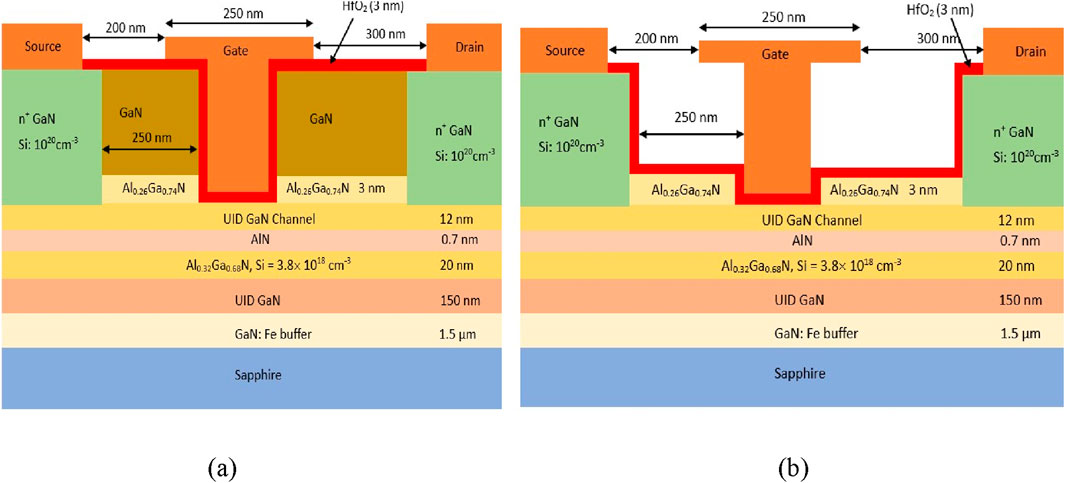
Figure 1. Cross-sectional schematic structure of AlGaN/GaN HEMT (a) with GaN cap layer (b) and without GaN cap Layer.
The Fermi-Dirac statistics model was employed to capture the effects of elevated doping levels, along with the Shockley–Read–Hall (SRH) recombination-generation model, and incomplete ionization models used, offered by Silvaco TCAD [26]. The SRH recombination model consists of four different stages: initially, electrons and holes are captured, followed by their subsequent emission. To manage the carrier transport field-dependent mobility and concentration-dependent mobility models were incorporated. Other essential models, including drift-diffusion, continuity, quantum tunneling, the high-field velocity saturation, and the Schrödinger-Poisson equations [27], were utilized to regulate electron and hole transport, as well as their dynamics throughout the simulations. Newton’s method was employed to solve the physics-based models over multiple triangular mesh regions of the HEMT. The simulation models were validated using experimentally data sample, as reported by Odabasi et al. [9]. Figure 2 shows that, the simulated results closely align with the experimental data, confirming the simulation environment feasible for comparative analysis.
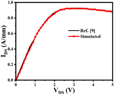
Figure 2. Calibration of the silvaco ATLAS TCAD tool. Output characteristics compared with reported data in [9].
3 Results and discussion
Figure 3 illustrates the impact of the GaN cap layer on the performance of high-electron mobility transistors. At VGS of 0 V and 2 V, HEMTs without the GaN cap layer exhibit higher IDS values, reaching 0.8 mA/μm and 0.99 mA/μm, and the corresponding to on-state resistance (Ron) of 1.02 Ω·mm and 0.88 Ω·mm, respectively. In contrast, devices with the cap layer achieve lower current densities of about 0.6 mA/μm and 0.85 mA/μm, corresponding Ron of 1.34 Ω·mm and 1.017 Ω·mm under the same conditions. The output characteristics shows a marked improvement in current density for devices without the GaN cap layer compared to the GaN cap layer. The GaN HEMT without a GaN cap layer enhances the saturation behavior, and reduces Ron, indicating better channel control and reduced short-channel effects. These improvements are due to enhanced electron mobility and reduced surface scattering, leading to superior electron transport characteristics.
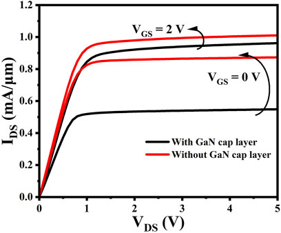
Figure 3. Variation of IDS as a function of VDS at VGS = 0 V and VGS = 2 V for AlGaN/GaN HEMTs with and without GaN cap layer.
Figure 4 presents the transfer characteristics of HEMTs with and without GaN cap layer, demonstrating the gate-source voltage (VGS) versus drain current (IDS) relationship. Measurements were taken at different drain-source voltages (VDS = 1 V, 4 V). As VGS increases from −5 V to 1 V, the GaN HEMTs show a steeper increase in IDS, and maximum current density (IDS_max) of 1.1 mA/μm at VDS = 4 V. In contrast, HEMTs with the GaN cap layer achieve a slightly lower peak current density under the same conditions. The threshold voltage is marginally shifted, indicating better channel control and reduced short-channel effects in devices with the GaN cap layer.
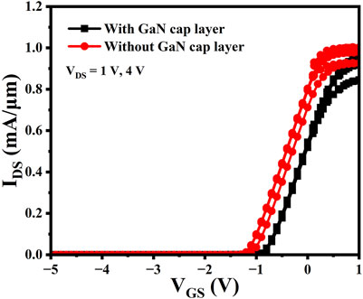
Figure 4. Transfer characteristics at VDS = 1 V and VDS = 4 V for GaN HEMTs with and without GaN cap layer.
Figure 5 shows the transconductance (gm) of GaN HEMTs with and without a GaN cap layer as a function of VGS at a constant VDS of 3 V. The transconductance curve for HEMTs without the GaN cap layer demonstrates a higher peak gm value compared to those with the GaN cap layer, indicating improved electron mobility and channel control in the absence of the GaN cap layer. The device without the GaN cap layer reaches a peak transconductance (gm_max) of 0.75 S/mm at VGS = −0.51 V, whereas the device with the GaN cap layer achieves a slightly lower peak gm_max. This improvement can be attributed to the absence of the GaN cap layer, which reduce surface scattering and traps, thereby enhancing the overall device performance.
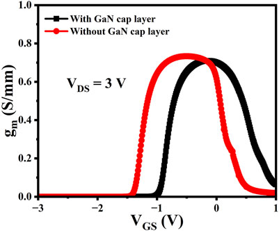
Figure 5. Transconductance (gm) characteristics of GaN HEMTs with and without GaN cap layer at VDS = 3 V.
Figure 6 shows cut-off frequency (fT) as a function of IDS with and without GaN cap layer at constant drain to source voltage of 3 V. The device without and with cap layer exhibits higher cut-off frequency (fT,max) of 183 GHz and 99.79 GHz, respectively. Both devices experience a decline in fT at high IDS, but the non-capped device maintains better performance. The GaN cap layer introduces parasitic effects that degrade RF performance. Thus, the without GaN cap configuration offers superior high-frequency behavior.
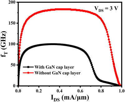
Figure 6. fT Vs IDS of GaN HEMTs with and without GaN cap layer at VDS = 3 V.
Figure 7 illustrates the output characteristics of GaN HEMTs without a GaN cap layer with varying drain doping concentrations (ND) from 1017 cm−3 to 1021 cm−3 at a constant VGS of 1 V. The results show a clear trend, as the doping concentration increases, the drain current (IDS) also increases. For ND = 1017 cm−3, the IDS reaches 0.385 mA/μm, whereas for ND = 1021 cm−3, IDS reaches nearly 0.97 mA/μm, indicating improved conductivity with higher doping levels. This enhancement in current with increasing doping is due to the higher carrier concentration, which reduces the resistance in the channel.
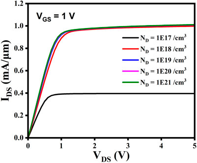
Figure 7. Variation of output characteristics for different drain doping concentrations at VGS = 1 V in GaN HEMTs without GaN cap layer.
Figure 8 illustrates the transfer characteristics of GaN HEMT for different drain doping concentrations at a constant VDS of 1 V. The drain concentrations (ND) range from 1017 cm−3 to 1022 cm−3. As the donor concentration increases the IDS also increases, and the maximum current of approximately 0.98 mA/μm around VGS = 0.5 V for ND = 1022 cm−3, due to the enhanced electron mobility and conductivity at higher doping levels. This behavior highlights how donor concentration improves device performance by increasing the current-carrying capability.
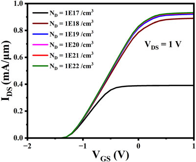
Figure 8. Variation of Transfer characteristics for different drain doping concentrations at VDS = 1 V in GaN HEMTs without GaN cap layer.
Figure 9 shows the transconductance (gm) characteristics as a function of VGS at a constant VDS = 3 V. The graph shows a significant change in gm for different ND levels. The higher donor concentrations result in higher peaks in transconductance. The result suggests that higher doping levels improve the device’s electrical characteristics by enhancing charge carrier mobility, thereby increasing the transconductance.
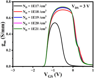
Figure 9. Variation of Transconductance (gm) characteristics for different drain doping concentrations at VDS = 3 V in GaN HEMTs without GaN cap layer.
From Figure 10 observed that the threshold voltage remains nearly constant at approximately −1.4 V for ND = 1017 cm−3 to ND = 1022 cm−3. This indicates that the threshold voltage is not significantly influenced by changes in donor concentration within this range. The stability of VTH suggests that the device maintains consistent switching characteristics regardless of variations in doping levels, which can be advantageous for ensuring uniform performance in applications where device consistency is crucial.
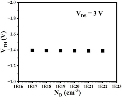
Figure 10. Variation of threshold voltage (VTH) for different drain doping concentrations at VDS = 3 V in GaN HEMTs without GaN cap layer.
Figure 11 illustrates the relationship between the cut-off frequency (fT) and the drain current density (IDS) for different doping at VDS = 3 V. These results indicate that the cut-off frequency is approximately same for ND = 1018/cm3 to for ND = 1022/cm3. At ND = 1017/cm3, the cut-off frequency reaches a peak value of 165 GHz. However, beyond this point, as IDS continues to increase, fT decreases significantly, due to parasitic effects such as self-heating or increased channel resistance. For ND = 1022/cm3, the maximum cut-off frequency of 183.8 GHz at VDS = 3 V.
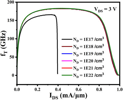
Figure 11. Variation of cut-off frequency (fT) for different drain doping concentrations at VDS = 3 V in GaN HEMTs without GaN cap layer.
To evaluate the significance of our findings, we performed a comparative analysis between GaN HEMTs without cap layer and state-of-the-art GaN HEMTs with cap layer. Table 1 presents the details of device parameters and performance metrics [9, 28, 29]. Our study highlights the exceptional DC performance of GaN HEMTs without GaN cap layer, achieving a peak drain current of 0.99 mA/μm at VGS = 2 V and a cut-off frequency of 183.8 GHz at VDS = 3 V. Additionally, the devices exhibit a notably low on-state resistance, which plays a critical role in reducing power losses and improving overall efficiency. These findings suggest that, GaN HEMT without GaN cap layer have the potential to surpass existing RF transistor performance limits, paving the way for next-generation semiconductor technology in high-frequency, and MEMS applications.
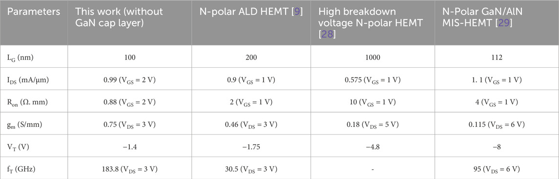
Table 1. Comparison between GaN HEMT without cap layer and state-of-the-art GaN HEMTs with cap layer.
4 Conclusion
In summary, we have investigated the performance of nanostructure N-polar AlGaN/GaN HEMTs with and without GaN cap layer, and focused on the effects of drain doping concentration. Devices without the GaN cap layer demonstrated improved electron mobility, reduced on-state resistance, and enhanced transconductance. The GaN HEMT without the cap layer achieved a peak drain current of 0.99 mA/μm and Ron of 0.88 Ω·mm at VGS = 2 V. Additionally, higher doping concentrations improved current density and transconductance, reaching a peak current of 0.98 mA/μm at ND = 1022 cm-3 at VDS = 1 V. The devices without the GaN cap layer exhibited enhanced high-frequency characteristics, with the maximum cut-off frequency reaching 183.8 GHz at VDS = 3 V. Thus, it is conclude that the N-polar GaN HEMTs without a GaN cap layer, show strong potential for high-power, high-frequency, and N/MEMS sensor applications. These finding is crucial for optimizing the doping levels in semiconductor devices to achieve desired electrical performance.
Data availability statement
The original contributions presented in the study are included in the article/supplementary material, further inquiries can be directed to the corresponding author.
Author contributions
CD: Investigation, Methodology, Validation, Writing – original draft. KM: Formal Analysis, Supervision, Writing – review and editing.
Funding
The author(s) declare that financial support was received for the research and/or publication of this article. The authors declare that the tools utilized for this research work was supported by TETRA-SERB scheme of the DST (Department of Science and Technology), Govt. of India, funded R&D Project bearing sanction number: TTR/2021/000102 (current status: Project completed), awarded to Prof.(Dr.) Kaushik Mazumdar (P.I.), IIT (ISM) Dhanbad, India.
Conflict of interest
The authors declare that the research was conducted in the absence of any commercial or financial relationships that could be construed as a potential conflict of interest.
Generative AI statement
The author(s) declare that no Gen AI was used in the creation of this manuscript.
Publisher’s note
All claims expressed in this article are solely those of the authors and do not necessarily represent those of their affiliated organizations, or those of the publisher, the editors and the reviewers. Any product that may be evaluated in this article, or claim that may be made by its manufacturer, is not guaranteed or endorsed by the publisher.
References
1. Chugh N, Kumar M, Bhattacharya M, Gupta RS. Sheet carrier concentration and current–voltage analysis of Al 0.15 Ga 0.85 N/GaN/Al 0.15 Ga 0.85 N double heterostructure HEMT incorporating the effect of traps. Microsystem Tech (2019) 28:665–74. doi:10.1007/s00542-019-04322-5
2. Dubey SK, Islam A. Impact of gate recessing on DC, RF and noise parameters of 6H-SiC-based Al0. 30Ga0. 70N/GaN HEMT for RF and low noise applications. Microsystem Tech (2023) 29(4):515–25. doi:10.1007/s00542-022-05362-0
3. Sinha K, Dubey SK, Islam A. Study of high Al fraction in AlGaN barrier HEMT and GaN and InGaN channel HEMT with in 0.17 Al 0.83 N barrier. Microsystem Tech (2020) 26:2145–58. doi:10.1007/s00542-019-04466-4
4. Gao Z, Romero MF, Calle F. Thermal and electrical stability assessment of AlGaN/GaN metal–oxide semiconductor high-electron mobility transistors (MOS HEMTs) with HfO2 gate dielectric. IEEE Trans Electron Devices (2018) 65(8):3142–8. doi:10.1109/ted.2018.2842205
5. Lalinsky T, Hudek P, Vanko G, Dzuba J, Kutiš V, Srnánek R, et al. Micromachined membrane structures for pressure sensors based on AlGaN/GaN circular HEMT sensing device. Microelectronic Eng (2012) 98:578–81. doi:10.1016/j.mee.2012.06.014
6. Tian Y, Shao Y. Mini-review on periodic properties of MEMS oscillators. Front Phys (2024) 12:1498185. doi:10.3389/fphy.2024.1498185
7. Hörberg M, Emanuelsson T, Ligander P, Lai S, Zirath H, Kuylenstierna D, et al. RF-MEMS tuned GaN HEMT based cavity oscillator for X-band. IEEE Microwave Wireless Components Lett (2016) 27(1):46–8. doi:10.1109/LMWC.2016.2629973
8. Qian MY, He CH, He JH. Enhanced piezoelectric performance of PVDF nanofibers by biomimicking the Spider’s long liquid transport. Chem Eng J (2024) 483:149159. doi:10.1016/j.cej.2024.149159
9. Odabasi O, Mohanty S, Khan K, Ahmadi E. N-polar GaN deep recess HEMT with atomic layer deposition HfO2 as gate insulator. IEEE Trans Electron Devices (2023) 70(9):4572–7. doi:10.1109/ted.2023.3295352
10. Hamwey R, Hatui N, Akso E, Wu F, Clymore C, Keller S, et al. First demonstration of an N-polar InAlGaN/GaN HEMT. IEEE Electron Device Lett (2023) 45:328–31. doi:10.1109/led.2023.3346818
11. Mohanty S, Sayed I, Jian ZA, Mishra U, Ahmadi E. Investigation and optimization of HfO2 gate dielectric on N-polar GaN: impact of surface treatments, deposition, and annealing conditions. Appl Phys Lett (2021) 119(4). doi:10.1063/5.0053886
12. Mohanty S, Diez S, Jian ZA, Ahmadi E. Design of ultra-scaled-channel N-polar GaN HEMTs with high charge density: a systematic study of hole traps and their impact on charge density in the channel. J Appl Phys (2020) 128(23). doi:10.1063/5.0019222
13. Rakoski S, Diez S, Li H, Keller S, Ahmadi E, Kurdak Ç. Electron transport in N-polar GaN-based heterostructures. Appl Phys Lett (2019) 114(16). doi:10.1063/1.5090233
14. Zheng X, Guidry M, Li H, Ahmadi E, Hestroffer K, Romanczyk B, et al. N-polar GaN MIS-HEMTs on sapphire with high combination of power gain cutoff frequency and three-terminal breakdown voltage. IEEE Electron Device Lett (2015) 37(1):77–80. doi:10.1109/led.2015.2502253
15. Romanczyk B, Li W, Guidry M, Hatui N, Krishna A, Wurm C, et al. N-polar GaN-on-Sapphire deep recess HEMTs with high W-band power density. IEEE Electron Device Lett (2020) 41(11):1633–6. doi:10.1109/led.2020.3022401
16. Li W, Romanczyk B, Guidry M, Akso E, Hatui N, Wurm C, et al. Record RF power performance at 94 GHz from millimeter-wave N-polar GaN-on-Sapphire deep-recess HEMTs. IEEE Trans Electron Devices (2023) 70(4):2075–80. doi:10.1109/TED.2023.3240683
17. Romanczyk B, Zheng X, Guidry M, Li H, Hatui N, Wurm C, et al. W-band power performance of SiN-passivated N-polar GaN deep recess HEMTs. IEEE Electron Device Lett (2020) 41(3):349–52. doi:10.1109/LED.2020.2967034
18. Kolluri SK. Establishing a design space and technology for RF N-polar aluminium gallium nitride/gallium nitride HEMTs. Santa Barbara, CA, USA: Univ. California (2011).
19. Romanczyk B, Guidry M, Zheng X, Li H, Ahmadi E, Keller S, et al. Bias-dependent electron velocity extracted from N-polar GaN deep recess HEMTs. IEEE Trans Electron Devices (2020). 67(4):1542–6. doi:10.1109/TED.2020.2973081
20. Guidry MT. Characterization, modeling, and design of N-polar GaN mm-wave power transistors. Santa Barbara, Santa Barbara, CA, USA: Univ. California (2017). Ph.D. thesis, Dept. Elect. Comput. Eng.
21. Moon JS, Grabar B, Wong J, Dao C, Arkun E, Tai H, et al. W-band graded-channel GaN HEMTs with record 45% power-added-efficiency at 94 GHz. IEEE Microwave Wireless Technology Lett (2022) 33(2):161–4. doi:10.1109/lmwc.2022.3207978
22. Ho SY, Lee CH, Tzou AJ, Kuo HC, Wu YR, Huang J. Suppression of current collapse in enhancement mode GaN-based HEMTs using an AlGaN/GaN/AlGaN double heterostructure. IEEE Trans Electron Devices (2017) 64(4):1505–10. doi:10.1109/ted.2017.2657683
23. Lee JH, Im KS, Lee JH. Effect of in-situ silicon carbon nitride (sicn) cap layer on performances of algan/gan mishfets. IEEE J Electron Devices Soc (2021) 9:728–34. doi:10.1109/jeds.2021.3100760
24. Yamada A, Minoura Y, Kurahashi N, Kamada Y, Ohki T, Sato M, et al. 31 W/mm at 8 GHz in InAlGaN/GaN HEMT with thermal CVD SiNx passivation. IEEE Electron Device Lett (2024) 45:324–7. doi:10.1109/led.2024.3355051
25. Yu L, Shao Z, Xu L, Wang M. High throughput preparation of aligned nanofibers using an improved bubble-electrospinning. Polymers (2017) 9(12):658. doi:10.3390/polym9120658
28. Koksaldi OS, Haller J, Li H, Romanczyk B, Guidry M, Wienecke S, et al. N-polar GaN HEMTs exhibiting record breakdown voltage over 2000 V and low dynamic on-resistance. IEEE Electron Device Lett (2018) 39(7):1014–7. doi:10.1109/LED.2018.2834
Keywords: HEMTs, 2DEG density, gm, quantum tunneling, cut-off frequency, output characteristics
Citation: Das C and Mazumdar K (2025) Investigation of the impact of the GaN cap layer on DC and RF performance in N-polar AlGaN/GaN HEMTs. Front. Phys. 13:1561573. doi: 10.3389/fphy.2025.1561573
Received: 16 January 2025; Accepted: 03 April 2025;
Published: 24 April 2025.
Edited by:
Ji-Huan He, Soochow University, ChinaReviewed by:
Fayu Wan, Nanjing University of Information Science and Technology, ChinaJyoti Kandpal, Graphic Era University, India
Copyright © 2025 Das and Mazumdar. This is an open-access article distributed under the terms of the Creative Commons Attribution License (CC BY). The use, distribution or reproduction in other forums is permitted, provided the original author(s) and the copyright owner(s) are credited and that the original publication in this journal is cited, in accordance with accepted academic practice. No use, distribution or reproduction is permitted which does not comply with these terms.
*Correspondence: Kaushik Mazumdar, a2F1c2hpa19lZHVAeWFob28uY28uaW4=