 Fajian Zhen
 Yunqing Liu1*
94% of researchers rate our articles as excellent or good
Learn more about the work of our research integrity team to safeguard the quality of each article we publish.
Find out more
ORIGINAL RESEARCH article
Front. Phys., 21 March 2025
Sec. Optics and Photonics
Volume 13 - 2025 | https://doi.org/10.3389/fphy.2025.1560761
The current spatial electromagnetic environment is complex and dynamic, with electromagnetic interference and pollution growing increasingly severe. Utilizing electromagnetic wave manipulation technology to absorb and convert waste electromagnetic energy into useful energy is of great research significance. This study presents a miniaturized, single-layer ultrathin metasurface absorber (MA) featuring frequency tunability and polarization insensitivity. The proposed MA is constructed from four groups of rotationally symmetric herringbone-shaped structures, mounted on a Rogers 438 substrate with a metallic ground plane. This design ensures efficient absorption of electromagnetic waves across all polarization angles, while the absorption frequency can be adjusted by modifying the dimensions of the herringbone structures. The device demonstrates an absorption coverage angle of ±60° for incident waves at various oblique angles. Unlike conventional absorbers that incorporate discrete resistors within each independent unit, the proposed MA integrates these components into a unified system. By employing resistors to interconnect adjacent unit cells, the design forms a cohesive absorber structure, significantly reducing the total number of resistors required. Full-wave simulations demonstrate nearly perfect absorption of electromagnetic waves across diverse polarization angles. The MA is highly compact, with a unit-cell dimension of only 0.16λ × 0.16λ and an ultra-thin profile of only 0.023λ. The newly developed MA holds promising potential for applications in integrated devices, energy harvesting systems, and radar cross-section assessments.
Electromagnetic absorbers are widely utilized in various applications, including stealth technology, reducing radar cross-section, energy harvesting and darkroom design, with the primary goal of minimizing the reflection and maximizing the absorption of incident electromagnetic waves [1–4].
However, traditional absorbers are often constrained by limitations in size, thickness, polarization insensitivity, and absorption efficiency [5]. Recent advancements in metamaterials have spurred the development of planar electromagnetic metasurfaces capable of achieving near-perfect absorption. A considerable number of studies have focused on overcoming the limitations associated with conventional absorbers by innovating electromagnetic metasurface designs [6–11]. Among these, circuit analog absorbers are excellent candidates for reducing the thickness of structures by introducing reactive elements. The integration of resistors enables the metasurface form a high-impedance surface that matches the impedance of free space, thereby achieving the absorption of incident waves. By leveraging the characteristics of resonant circuits to match the properties of the conductor backing substrate, the thickness is reduced, and the current is effectively dissipated through the resistors, resulting in enhanced absorption properties.
To improve key attributes such as size, thickness, polarization angle, and incident angle, researchers have delved into the design of multilayer absorbers, incorporated air layers between multilayer substrates, and integrated lumped resistors within the metasurfaces structures [12–14]. A notable advancement is the proposal of a double-layer absorber characterized by a compact thickness and a square loop structure, where resistors are embedded within the square loop and distributed across the two substrate layers. This design achieves a substrate thickness of 0.087λ, but requires a unit size of 0.46λ. Each unit requires the integration of 16 resistors, and the inclusion of an air layer in the multilayer configuration results in an overall thickness of 0.6λ [12]. In [13], the dimensions were further minimized to a size of 0.4λ and a thickness of 0.24λ; however, the requirement for 16 resistors per unit persisted, and the design exhibited limited incident angle insensitivity, effective only up to 30°. Subsequent research introduced a rotationally symmetric bent metal strip structure, an air layer was inserted between the lossy layer and the metal ground plane, achieving a thickness of 0.089λ and reducing the unit size to 0.2λ, with 8 resistors integrated per unit [14]. In an attempt to eliminate the air layer and reduce the number of resistors, researchers have investigated single-layer absorber designs [15–19]. One notable design is a double-ring structure integrating 8 resistors, which successfully eliminates the air layer while reducing the single-layer thickness to 5 mm [15]. Another study proposed a single-layer absorber with a thickness of 0.077λ, which reduced the number of integrated resistors per unit to 4 [16]. Although certain single-layer configurations can achieve a thickness of 3 mm, they still necessitate the integration of more than 8 lumped resistors [17, 18]. Reference [19] proposed an asymmetric single-layer absorber that only integrates three resistors, reducing the unit size to 0.22λ and the thickness to 0.07λ; however, the inherent asymmetry of this design leads to variations in polarization angle insensitivity, and its performance with respect to incident angle insensitivity remains unaddressed. Current single-layer absorber technologies have successfully eliminated the air layer and reduced thickness, but often at the cost of increased unit size and a higher number of integrated lumped resistors. Larger MAs are both expensive to make and limit the application scenarios. Additionally, integrating more lumped resistors increases design complexity and complicates the resistor assembly process. Therefore, there is a pressing need to develop single-layer absorbers that achieve both compact unit sizes and reduced resistor counts while maintaining optimal performance.
In this paper, to reduce the thickness and minimize the number of concentrated resistors, we designed a novel MA based on a herringbone-shaped rotationally symmetric structure, which consists of a metasurface structure, a dielectric substrate and a bottom metallic ground plane. The metasurface unit-cell structure is designed with four rotationally symmetric herringbone-shaped slots, ensuring polarization-insensitive performance. Unlike conventional designs that integrate resistors within individual unit cells, the resistor elements in this design are strategically placed between adjacent metasurface units. This configuration significantly reduces the number of resistors required and minimizes the overall device size. The designed single-layer MA achieves a compact design with a thickness of 0.023λ and a unit cell period of 0.16λ, while maintaining polarization insensitivity and a wide incident angle absorption range of up to 60°. Finally, samples were made and the absorption performance of the MA was verified by testing.
The schematic diagram of the proposed MA is illustrated in Figure 1a. It consists of a dielectric substrate loaded with resistors and periodic metal electric resonators and a metal floor on the back. Figure 1b displays a structural diagram of a four-unit arrangement, detailing the distribution of resistance. The top view of the unit cell is presented in Figure 1c. The incorporation of a herringbone rotational symmetry structure facilitates polarization insensitivity. Each unit cell can be conceptualized as an equivalent RLC resonant circuit, which effectively absorbs incident electromagnetic waves and transforms them into electrical energy, subsequently dissipated by the lumped resistor. The proposed metasurface uses Rogers 438 with a dielectric constant of 4.38 and a loss tangent of 0.005 as the dielectric substrate. The simulation calculation is carried out in full-wave simulation software. By setting periodic boundary conditions and Floquet port excitation, the relevant absorption characteristic results are obtained.
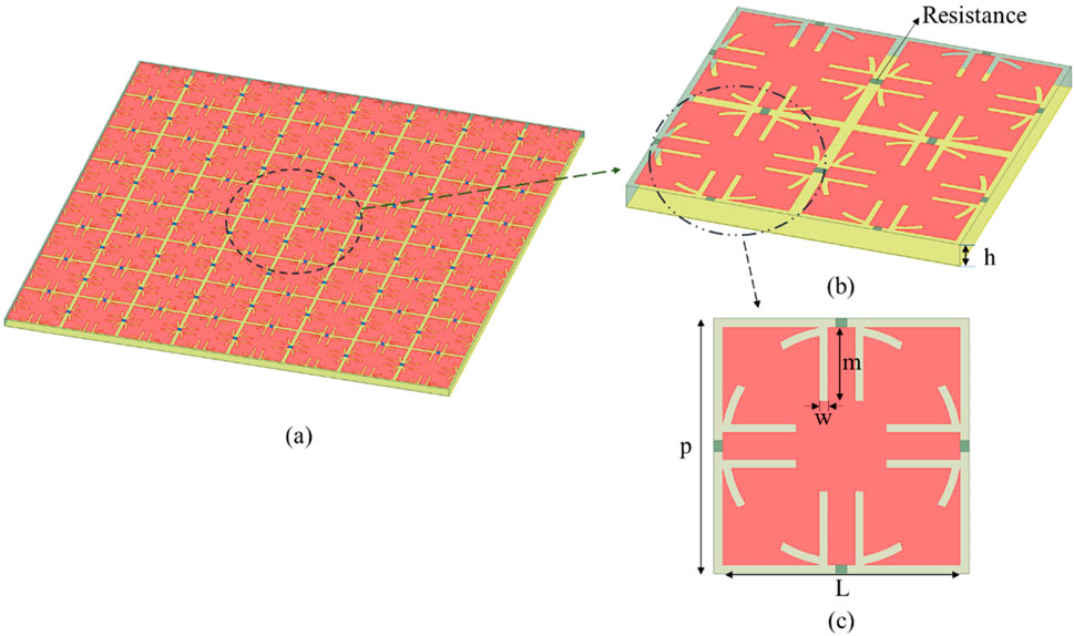
Figure 1. Proposed MA: (a) Overall structure. (b) Three dimensional geometry of the four unit-cell. (c) Top view of a unit-cell.
From the matching impedance theory, we can get Formula 1:
When the equivalent impedance of the metasurface
The absorption efficiency
Formula 2 can be expressed using S parameters as Formula 3:
Since the back of the MA is set by a metal plate, the transmission coefficient
The dielectric constant of the substrate has a significant effect on the size of the device, mainly due to the influence of wavelength. The relationship between the wavelength and the relative dielectric constant is expressed by the Formula 5:
Among them,
The unit-cell structure is shown in Figure 1b, comprises four herringbone-shaped rotationally symmetric elements. The unit size is 10.85 mm (0.16λ) × 10.58 mm (0.16λ), and the thickness is only 1.5 mm (0.023λ). To minimize the number of resistor elements, each unit cell shares a resistor with its adjacent units, ensuring that all units are interconnected through resistors. This design integrates the absorber into a unified system rather than operating as isolated units, thereby not only reducing the total number of resistors but also contributing to a more compact overall structure. The detailed parameter values of the unit cell are provided in Table 1.

Table 1. The parameters of the designed MA.
The unit-cell structure was simulated and analyzed based on the periodic boundary conditions in the full-wave simulation software. Initially, the S-parameters of the design were calculated, as shown in Figure 2a, where the incident angle is 0° and the polarization is TE mode. By adjusting the length of the microstrip line, the absorber can be tuned to operate in different frequency bands. This tunability arises because the grooves on both sides of the microstrip line function as equivalent capacitors, and the capacitance value directly influences the resonant frequency. This frequency-adjustable feature enables researchers to efficiently design absorbers tailored to specific target frequency bands. The ring groove structure with appropriate angles and the appropriate resistance value can deepen the resonance depth of the absorber. As illustrated in Figures 2b, c, the absorber exhibits minimal reflection when the ring groove angle is set to 10° and the resistance value is 400 Ω. Figure 2d presents the absorption efficiency of the absorber, demonstrating that the designed structure achieves an absorption efficiency exceeding 90% within the frequency range of 4.63–5.07 GHz, with a dielectric thickness of 1.5 mm. Furthermore, perfect absorption (100%) is achieved at 4.85 GHz.
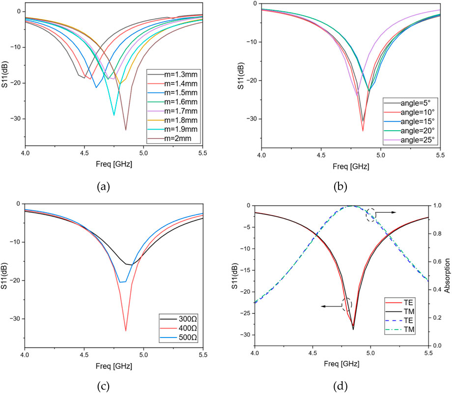
Figure 2. The impact of different parameters on design (a) microstrip line length. (b) Circular angle. (c) Resistance (d) S11 and absorption corresponding to different polarizations.
Figure 3 illustrates the equivalent circuit of the designed MA. The input port represents the incident wave in free space, the characteristic impedance of free space is 377Ω, R denotes the lumped resistance between adjacent unit-cells, L represents the inductance induced by the MA unit, C1 corresponds to the capacitance generated by the herringbone-shaped gap within the MA unit, C2 signifies the capacitance generated between adjacent units, C3 indicates the capacitance formed between the MA and the metallic ground plane, and Sub represents the dielectric substrate. Among them, C1 = 0.15pF, C2 = 0.212pF, C3 = 0.218pF, and L = 15.8 nH. The equivalent circuit was simulated using circuit simulation software, and the results were compared with those obtained from full-wave simulations. As depicted in Figure 4a, the reflection coefficients of the MA unit derived from the full-wave simulation exhibit excellent agreement with those of the equivalent circuit model. This consistency validates the accuracy of the equivalent circuit model in explaining the absorption mechanism of the MA. Furthermore, Figure 4b demonstrates that the real part of the impedance of the designed absorber within the absorption band is 377Ω, and the imaginary part approaches 0. This indicates that the absorber achieves optimal impedance matching with free space, thereby enabling perfect absorption. To validate the correctness of the resistor configuration, we compared the absorption capabilities of the designed metasurface for incident waves with and without the inclusion of resistors, as illustrated in Figure 5. It can be observed that, under both TE and TM modes, the absorption efficiency approaches 1 when resistors are incorporated, whereas the absorption efficiency remains below 0.2 in the absence of resistors. Therefore, the resistor configuration in this design significantly enhances the absorption efficiency.
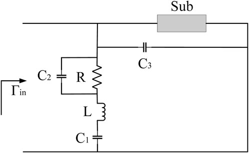
Figure 3. Equivalent circuit model.
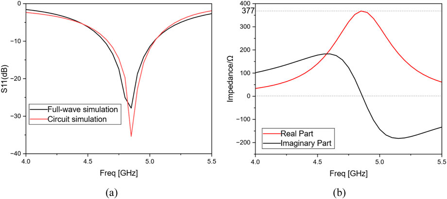
Figure 4. (a) Comparison of reflection coefficient of full-wave simulation and equivalent circuit. (b) Equivalent impedance of metasurface.
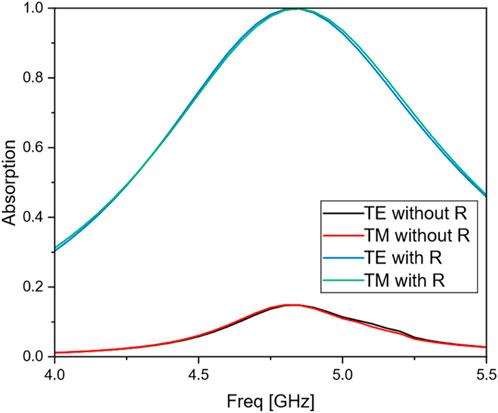
Figure 5. Effect of resistance on absorption efficiency.
To gain deeper insights into the operational mechanism and current distribution of the designed absorber, simulations were performed to analyze the surface current distribution on the metasurface absorption layer under both transverse electric (TE) and transverse magnetic (TM) polarization states at a frequency of 4.85 GHz. The results, depicted in Figures 6a, b, reveal significant resonance phenomena in both TE and TM polarization modes, indicating that the designed absorber exhibits polarization insensitivity. Under varying polarization states, current flows along both the X- and Y-axes. Resistors are strategically positioned along these axes, interconnecting all units to facilitate the flow of current through the resistors across the entire metasurface. In this configuration, the absorbed energy is effectively collected and dissipated within the surface layer. This design offers the advantage of facilitating targeted energy collection rather than uncontrolled energy loss, thereby enhancing the overall efficiency of the absorber. This design offers the advantage of facilitating targeted energy collection rather than uncontrolled energy loss, thereby enhancing the overall efficiency of the absorber.
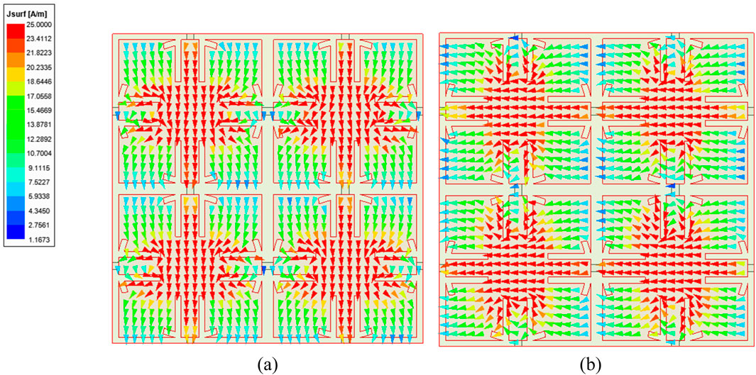
Figure 6. Surface current distribution (a) TM. (b) TE.
During the long-distance propagation of electromagnetic waves, both the polarization state and the angle of incidence may vary unpredictably. Consequently, to ensure efficient absorption of incident waves, it is essential to achieve polarization insensitivity and wide-angle stability. As demonstrated in Figure 7, the absorber exhibits nearly 100% absorption efficiency for incident waves at any polarization angle. Wide incident angle stability can improve the spatial absorption coverage of the absorber. Figure 8 illustrates the absorption efficiency under oblique incidence for different polarization states. For TE-polarized waves, the absorber maintains an absorption efficiency exceeding 90% across the entire frequency band for incident angles ranging from 0° to 45°. Even when the angle increases to 60°, the absorption efficiency remains above 80%. For TM-polarized waves, although the frequency of the absorption peak shifts slightly, the absorption efficiency still surpasses 95%. This combination of wide-angle stability and high absorption efficiency is unparalleled in other single-layer absorbers.
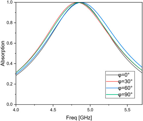
Figure 7. Absorption efficiency at different polarization angles (theta = 0°).
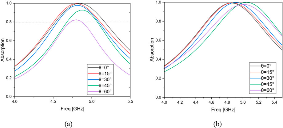
Figure 8. Absorption efficiency at different incidence angles for different polarization modes. (a) TE. (b) TM.
To evaluate the absorption capability of the designed absorber, a measurement setup was established using two horn antennas positioned on opposite sides of the absorber, as illustrated in Figure 9. The absorption capability was assessed by analyzing the S21 parameters of the horn antennas, with a metal plate of identical dimensions used as a reference for comparison. The findings are presented in Figure 10, the existence of the absorber absorbs most of the incident energy and effectively reduces reflection. Figure 11 displays the dual-station RCS results for angles ranging from −90° to 90°. The results indicate that the RCS of the absorber remains consistently lower than that of the metal plate across all measured angles, thereby confirming that the incident waves are absorbed rather than scattered in other directions.
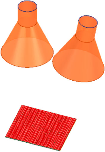
Figure 9. Metasurface absorber wave absorption scene simulation diagram.
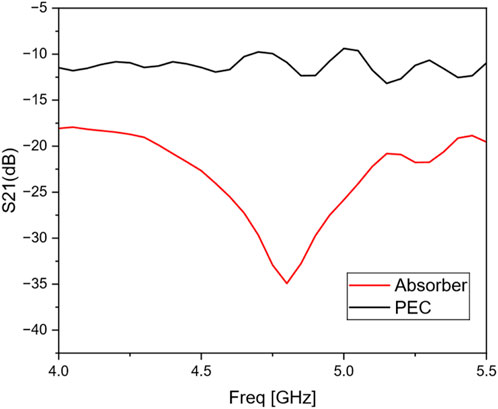
Figure 10. S21 comparison between absorber and PEC.
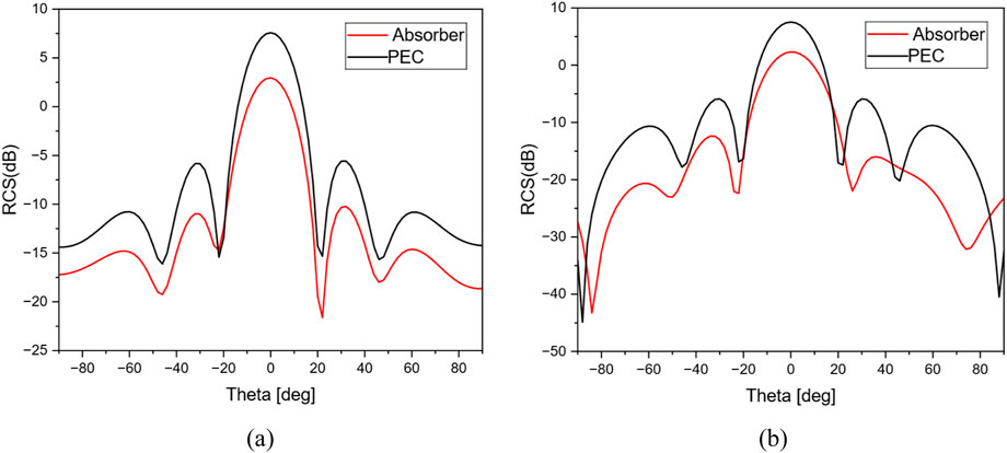
Figure 11. Bi-static RCS of the absorber for (a) vertical and (b) horizontal polarized incident waves at 4.85 GHz.
A 10 × 10 absorber array was fabricated using a dielectric substrate with a relative permittivity of 4.38, a loss tangent of 0.005, and a thickness of 1.5 mm. The resistors, with a package size of 0603, were integrated into the structure as shown in Figure 12c. The overall dimensions of the fabricated device 105 × 105 mm, and resistors were loaded between each pair of adjacent unit cells. The absorption performance of the absorber was measured using the free-space method. Two standard horn antennas were employed to measure the reflection coefficient, with one antenna functioning as the transmitter and the other as the receiver. Both antennas were positioned 1 m away from the absorber and tilted approximately 5° relative to the normal axis of the absorber, as depicted in Figure 12a. In Figure 12b, to mitigate environmental reflections, a conical absorbing material was positioned around the absorber. As shown in Figure 13, the designed absorber achieves near-ideal absorption efficiency within the frequency range of 4–5.5 GHz, with the measured results exhibiting excellent agreement with the simulation results. Minor discrepancies observed in the measurements can be attributed to tolerances in resistor soldering and the precise positioning of the horn antennas. Minor discrepancies observed in the measurements can be attributed to tolerances in resistor soldering and the precise positioning of the horn antennas.

Figure 12. Photographs of the prototype and measurement system. (a) Measurement setup; (b) Perspective of the overall MA; (c) Enlarged of the MA.
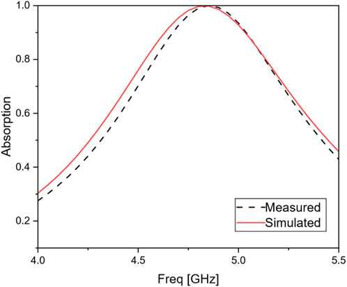
Figure 13. Simulated and measured absorptivity plot.
Table 2 presents a comparative analysis of the proposed absorber in relation to existing literature. It can be seen from the table that compared with other studies, our proposed absorber has reduced thickness, fewer resistors under a single-layer design, and a larger oblique angle of incidence.
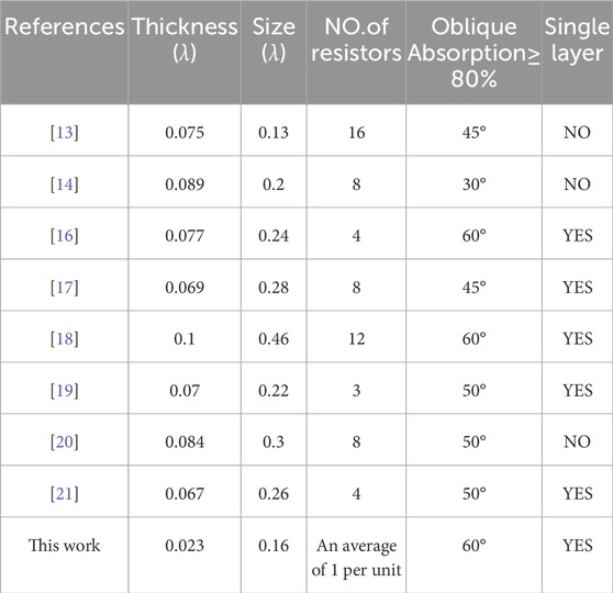
Table 2. Comparison between the proposed absorber and previously reported absorber.
In this study, we successfully designed and realized a single-layer, ultra-thin, low-resistor-count, wide-angle, and polarization-insensitive metasurface absorber based on a rotationally symmetric herringbone architecture and a strategic resistor arrangement. The rectangular gaps within the herringbone structure enable tunability of the absorption frequency band, providing researchers with the flexibility to tailor the design according to specific requirements. The interconnected resistor layout makes the metasurface absorber a whole, significantly reducing resistor usage while expanding its potential applications, particularly in the field of energy harvesting. The proposed metasurface absorber exhibits polarization insensitivity across angles of 0°–90° and maintains an absorption efficiency exceeding 80% at oblique incidence angles of up to 60°. The design was experimentally validated through the fabrication and testing of a prototype. Future research will focus on advancing the development of broadband and multi-band metasurface absorbers, aiming to realize broadband or multi-band functionality within a single-layer, low-resistor-count framework.
The original contributions presented in the study are included in the article/supplementary material, further inquiries can be directed to the corresponding author.
FZ: Writing–original draft, Writing–review and editing. YL: Writing–review and editing. JD: Writing–review and editing. SK: Writing–review and editing.
The author(s) declare that no financial support was received for the research, authorship, and/or publication of this article.
The authors declare that the research was conducted in the absence of any commercial or financial relationships that could be construed as a potential conflict of interest.
The author(s) declare that no Generative AI was used in the creation of this manuscript.
All claims expressed in this article are solely those of the authors and do not necessarily represent those of their affiliated organizations, or those of the publisher, the editors and the reviewers. Any product that may be evaluated in this article, or claim that may be made by its manufacturer, is not guaranteed or endorsed by the publisher.
1. Qu S, Sheng P. Microwave and acoustic absorption metamaterials. Phys Rev Appl (2022) 17(4):047001. doi:10.1103/physrevapplied.17.047001
2. He ZJ, Deng L, Zhang P, Liu Y, Yan T, Liao C, et al. Wideband high-efficiency and simple-structured rectifying metasurface. IEEE Trans Antennas Propagation (2023) 71(7):6202–7. doi:10.1109/tap.2023.3269862
3. Yao W, Gao H, Tian Y, Wu J, Guo L, Huang X. Wideband low-RCS linear polarized array based on miniaturized polarization conversion metasurface. IEEE Trans Antennas Propagation (2023) 71(7):5663–74. doi:10.1109/tap.2023.3270383
4. Saqlain M, Baqir MA, Choudhury PK. MXene-and graphene-assisted THz metamaterial for cancer cells detection based on refractive index sensing. IEEE Trans Nanotechnology (2024) 23:652–7. doi:10.1109/tnano.2024.3458427
5. Tirkey MM, Gupta N. Electromagnetic absorber design challenges. IEEE Electromagn Compatibility Mag (2019) 8(1):59–65. doi:10.1109/memc.2019.8681370
6. Bilal RMH, Baqir MA, Choudhury PK, Karaaslan M, Ali MM, Altlntas O, et al. Wideband microwave absorber comprising metallic split-ring resonators surrounded with E-shaped fractal metamaterial. IEEE Access (2021) 9:5670–7. doi:10.1109/access.2020.3048927
7. Bilal RMH, Baqir MA, Iftikhar A, Ali M, Rahim A, Akhtar MN, et al. A novel omega shaped microwave absorber with wideband negative refractive index for C-band applications. Optik (2021) 242:167278. doi:10.1016/j.ijleo.2021.167278
8. Bilal RMH, Baqir MA, Iftikhar A, Naqvi SA, Mughal MJ, Ali MM. Polarization-controllable and angle-insensitive multiband Yagi-Uda-shaped metamaterial absorber in the microwave regime. Opt Mater Express (2022) 12(2):798–810. doi:10.1364/ome.451073
9. Hannan S, Islam MT, Faruque MRI, Rmili H. Polarization-independent perfect metamaterial absorber for C, X and, Ku band applications. J Mater Res Technology (2021) 15:3722–32. doi:10.1016/j.jmrt.2021.10.007
10. Yu P, Besteiro LV, Huang Y, Wu J, Fu L, Tan HH, et al. Broadband metamaterial absorbers. Adv Opt Mater (2019) 7(3):1800995. doi:10.1002/adom.201800995
11. Verma A, Meena OP. A review of metamaterial absorber and its absorption techniques[C]//2023 IEEE international students. In: Conference on Electrical, Electronics and Computer Science (SCEECS). IEEE (2023). p. 1–6.
12. Yao Z, Xiao S, Li Y, et al. On the design of wideband absorber based on multilayer and multiresonant FSS array. IEEE Antennas Wireless Propagation Lett (2020) 20(3):284–8. doi:10.1109/LAWP.2020.3046010
13. Yao Z, Xiao S, Jiang Z, Yan L, Wang BZ. On the design of ultrawideband circuit analog absorber based on quasi-single-layer FSS. IEEE Antennas Wireless Propagation Lett (2020) 19(4):591–5. doi:10.1109/lawp.2020.2972919
14. Zhang B, Jin C, Shen Z. Low-profile broadband absorber based on multimode resistor-embedded metallic strips. IEEE Trans Microwave Theor Tech (2019) 68(3):835–43. doi:10.1109/tmtt.2019.2956933
15. Yuan W, Cheng Y. Low-frequency and broadband metamaterial absorber based on lumped elements: design, characterization and experiment. Appl Phys A (2014) 117:1915–21. doi:10.1007/s00339-014-8637-3
16. Kundu D, Mohan A, Chakrabarty A. Single-layer wideband microwave absorber using array of crossed dipoles. IEEE Antennas Wireless Propagation Lett (2016) 15:1589–92. doi:10.1109/lawp.2016.2517663
17. Weng C, Yang X, Li X. Ultrathin broadband dual-ring metamaterial absorber based on chip resistance. physica status solidi (a) (2023) 220(7):2200795. doi:10.1002/pssa.202200795
18. Barde C, Gupta NK, Ranjan P, Roy K, Sinha R. Angle-independent wideband metamaterial microwave absorber for C and X band application. Int J Microwave Wireless Tech (2024) 16(1):101–9. doi:10.1017/s1759078723000685
19. Islam KMR, Rahimian A, Machado GG, Ali Babar Abbasi M, Ahmad Cheema A, Meenan BJ. Design and experimental performance evaluation of a single-layer polarization-insensitive asymmetric microwave metasurface absorber. IEEE Trans Antennas Propagation (2024) 72:6520–9. doi:10.1109/tap.2024.3424952
20. Zhang Y, Yang W, Li X, Liu G. Design and analysis of a broadband microwave metamaterial absorber. IEEE Photon J (2023) 15(3):1–10. doi:10.1109/jphot.2023.3277449
Keywords: miniaturized, absorber, polarization-insensitive, metasurface, energyharvester
Citation: Zhen F, Liu Y, Dong J and Kong S (2025) Miniaturized single layer ultra-thin polarization insensitive metasurface absorber. Front. Phys. 13:1560761. doi: 10.3389/fphy.2025.1560761
Received: 14 January 2025; Accepted: 10 March 2025;
Published: 21 March 2025.
Edited by:
Yu Luo, Tianjin University, ChinaReviewed by:
Muhammad Abuzar Baqir, COMSATS University Islamabad, Sahiwal campus, PakistanCopyright © 2025 Zhen, Liu, Dong and Kong. This is an open-access article distributed under the terms of the Creative Commons Attribution License (CC BY). The use, distribution or reproduction in other forums is permitted, provided the original author(s) and the copyright owner(s) are credited and that the original publication in this journal is cited, in accordance with accepted academic practice. No use, distribution or reproduction is permitted which does not comply with these terms.
*Correspondence: Yunqing Liu, bXpsaXV5dW5xaW5nQDE2My5jb20=
Disclaimer: All claims expressed in this article are solely those of the authors and do not necessarily represent those of their affiliated organizations, or those of the publisher, the editors and the reviewers. Any product that may be evaluated in this article or claim that may be made by its manufacturer is not guaranteed or endorsed by the publisher.
Research integrity at Frontiers
Learn more about the work of our research integrity team to safeguard the quality of each article we publish.