 Yu-Ze Sun†
 Yun-Ze Long
- Innovation Institute for Advanced Nanofibers, College of Physics, Shandong Key Laboratory of Medical and Health Textile Materials, Qingdao University, Qingdao, China
NiO/ZnO semiconductor heterostructures were fabricated via electrospinning to investigate their resistance behavior under varying magnetic fields. The resistance of the heterostructures was measured at different temperatures and in magnetic fields of varying strength and direction. Resistance spikes of 1.3%, 5.2%, and 10.7% were observed at 300 K, 290 K, and 280 K, respectively. These resistance variations were found to be influenced by both the magnetic field magnitude and direction, as well as light illumination. The observed phenomena are attributed to the interaction between the heterojunction and the magnetic field, alongside changes in spin electron orientation. This study demonstrates the potential of combining heterostructures and magnetic fields to modulate resistance, offering promising applications for optoelectronic and magnetoelectronic devices.
1 Introduction
Magnetic semiconductors are intriguing materials in spintronics, combining magnetic and semiconductor properties within a single material. Charge and spin are two intrinsic properties of electrons. Semiconductor technology based on the charge property of electrons and spintronics based on the spin property of electrons play crucial roles in contemporary information processing and storage domains [1, 2]. Semiconductors are essential for high-capacity information processing and communication devices, whereas multilayered magnetic metals and insulators play a crucial role in information storage devices [3, 4]. Research on materials with dual functionality for information processing and storage will drive the development of advanced electronic devices.
To further investigate the magnetic properties of these materials, it is necessary to change the external environment. Temperature variations, light illumination, and magnetic fields can modulate the resistivity of magnetic semiconductors. Temperature variations significantly impact the resistivity and magnetism of materials. For semiconductor materials, resistance increases with decreasing temperature, which is opposite to the behavior observed in metals [5]. In contrast, for magnetic materials, lower temperatures result in reduced thermal motion, leading to less disruption of electron arrangements in a magnetic field and exhibiting stronger magnetism [6, 7]. Therefore, studying the resistivity of magnetic semiconductors at various temperatures is of great research value.
Light illumination also significantly impacts the number of free electrons and their spin orientation within materials [8]. Semiconductor materials can utilize light to excite electrons and generate photo-induced charge carriers, resulting in changes in resistance [9, 10]. The influence of electron spin on the resistivity of magnetic materials can be modulated through magnetic field control, including giant magnetoresistance (MR) effects [11], magnetoelectric coupling [12, 13], phase separation [14], and magnetically tunable chiral ionic currents [15]. Research on manipulating magnetism through light excitation includes optically induced Hall effects [16–18] and optically generated spin-polarized currents [19]. Furthermore, the study of magnetically controlled transverse photovoltaic effects [20–24] and the enhancement of photocatalysis by magnetic fields [25] indicates significant research potential in the interplay between light and magnetism.
In addition to altering the external environment, the performance of materials can also be influenced by their design [26, 27]. For example, Das and Srinivasan demonstrated the presence of oxygen vacancy defects in ZnO and proposed evidence for oxygen defect-induced ferromagnetism in thermally treated electrospun zinc oxide nanowires [28]. The morphology of materials and the formation of heterogeneous structures can both impact their magnetic and resistive properties. Siddique and Tripathi discovered that the formation of more oxygen vacancies in nickel oxide at the nanoscale can lead to the emergence of ferromagnetic regions in antiferromagnetic nickel oxide [29]. NiO/ZnO nanofiber heterostructures have been utilized for various applications, including volatile organic compound sensing [30], anode materials for advanced lithium-ion batteries [31] and photocatalysis [32]. Magnetic nanofibers also have applications in nanoscale photodetectors, electromagnetic interference shielding, magnetic separation, tissue engineering, and nanogenerators [33, 34].
Constructing heterostructures is a powerful strategy for material enhancement, and nanoscale heterostructured materials have unique advantages. The rapid recombination of photogenerated holes and electrons within the catalyst affects its photocatalytic efficiency. Li et al. found that an energy gradient formed by doping heterostructures in NiO/ZnO nanofibers can further improve catalytic efficiency in semiconductor internal components [35, 36]. Additionally, Zhou and his colleagues found that magnetic-nonmagnetic heterostructures can prolong the lifetime of spin electrons [28, 37]. However, there is still insufficient research on the resistance changes of NiO/ZnO heterostructures in a magnetic field.
Based on the above background, we prepared NiO/ZnO heterostructures. By conducting resistance measurements in a magnetic field on the NiO/ZnO magnetic semiconductor material, we discovered resistance spikes in response to varying magnetic fields. Building on this, we investigated the effects of temperature, light exposure, and magnetic fields on this phenomenon. This anomalous resistance spike indicates changes in the heterojunction and electronic states within the sample, which is of significant importance for understanding the properties and applications of magnetic semiconductor materials [37]. By investigating resistance spikes in magnetic fields and opto-magnetic interactions in magnetic semiconductor materials, we aim to promote the development of new optoelectronic and magnetoelectronic devices, with the potential to enhance information processing and storage technologies.
2 Experimental details
2.1 Materials
Nickel acetate (Ni(CH3COO)2) and Dihydrate zinc acetate (Zn(CH3COO)2·2H2O) were acquired from Shanghai Zhanyun Chemical Co., Ltd. Anhydrous ethanol was provided by Sinopharm Chemical Reagent Co., Ltd. Polyvinylpyrrolidone (PVP) came from Sigma Aldrich Co., Ltd.
2.2 Preparation method
First, Zn(CH3COO)2 and Ni(CH3COO)2, with a molar ratio of 1:1 for Zn/Ni atoms, were separately added into glass bottles. Subsequently, 9 g of anhydrous ethanol and 1 g of PVP were added to prepare the electrospinning precursor solution. During the electrospinning process, a rotating drum served as the collector. Electrospinning was conducted using a voltage of 10 kV and a feed rate of 1 mL h-1. The resulting nanofiber membrane was then subjected to calcination in a muffle furnace. The temperature was increased at a rate of 3 °C min-1 until reaching 700°C, where it was held for 2 h. This process yielded a micro-nanostructure.
Finally, a low-temperature conductive silver glue was employed to attach conductive leads to an ITO-coated glass. The obtained micro/nanostructures was fixed onto the conductive glass to create the NiO/ZnO optoelectronic device. Additionally, single NiO and ZnO micro/nanostructures were also prepared as controls.
2.3 Characterization
X-ray diffraction (XRD; Rigaku SmartLab) was used to analyze the type and phase composition of the samples. Scanning electron microscopy (SEM, Phenom Pro G6, Thermo Fisher Scientific) was employed to study the crystal morphology of the samples. The comprehensive physical property measurement system (PPMS-9; Quantum Design) with Electronic Transport Option (ETO) was used to investigate the variation of resistance with the magnetic field in the samples. Lasers with wavelengths of 450 nm (blue light) and 635 nm (red light) were used for illumination. The direction of the applied magnetic field was parallel to the direction of lighting and the direction of the current, as shown in Figure 1.
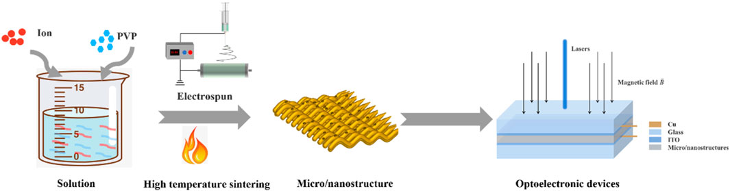
Figure 1. Schematic illustration of micro/nanostructure preparation and optoelectronic devices.
2.4 Detailed analysis methods
2.4.1 XRD
The crystal structure was characterized via powder X-ray diffraction with a Cu Kα radiation (λ = 1.5408 Å) source in the 2θ range of 25°–90° and a scanning rate of 5°/min.
2.4.2 SEM
SEM measurements were performed using a Phenom Pro G6 scanning electron microscope at an acceleration voltage of 15 kV, with the samples coated with a gold film to enhance conductivity.
2.4.3 Resistance
The experiment utilized the Electrical Transport Option (ETO) of the PPMS to measure resistance using the Ohmic method. Conductive silver paste was applied to form electrical contacts, and a two-wire method was employed for alternating current (AC) measurements with an applied voltage of 10 V and a frequency of 1 Hz.
2.4.4 Magnetization-temperature (M-T) measurement
The M-T measurements were conducted using the Vibrating Sample Magnetometer (VSM) module of the PPMS. The measurements included zero-field cooling (ZFC), where no magnetic field was applied during the cooling process, and field cooling (FC), where a magnetic field of 1,000 Oe was applied during cooling. In both ZFC and FC conditions, M-T tests were performed during warming under a magnetic field of 1,000 Oe in the temperature range of 3–380K.
3 Results and discussion
3.1 Experimental results
The morphology of the samples was analyzed by scanning electron microscopy (SEM) (Supplementary Figures S1, S2 and Figure 2A). In particular, the NiO/ZnO heterostructures exhibit an obvious network structure, indicating that the specific surface area is large, the defect density is high, and the ring current can be induced in the changing magnetic field (Figure 2A). X-ray diffraction (XRD) analysis (Figure 2B) shows diffraction peaks of ZnO at 31.66°, 34.36°, 36.16°, 47.46°, and 56.5°, corresponding to the (100), (002), (101), (102), and (110) crystal planes, respectively. Similarly, the XRD peaks of pure NiO are located at 36.82° and 42.9°, corresponding to the (111) and (200) crystal planes, confirming the cubic phase of NiO. No impurity peaks were observed in the XRD data of the sample, indicating successful preparation of NiO/ZnO heterostructures.
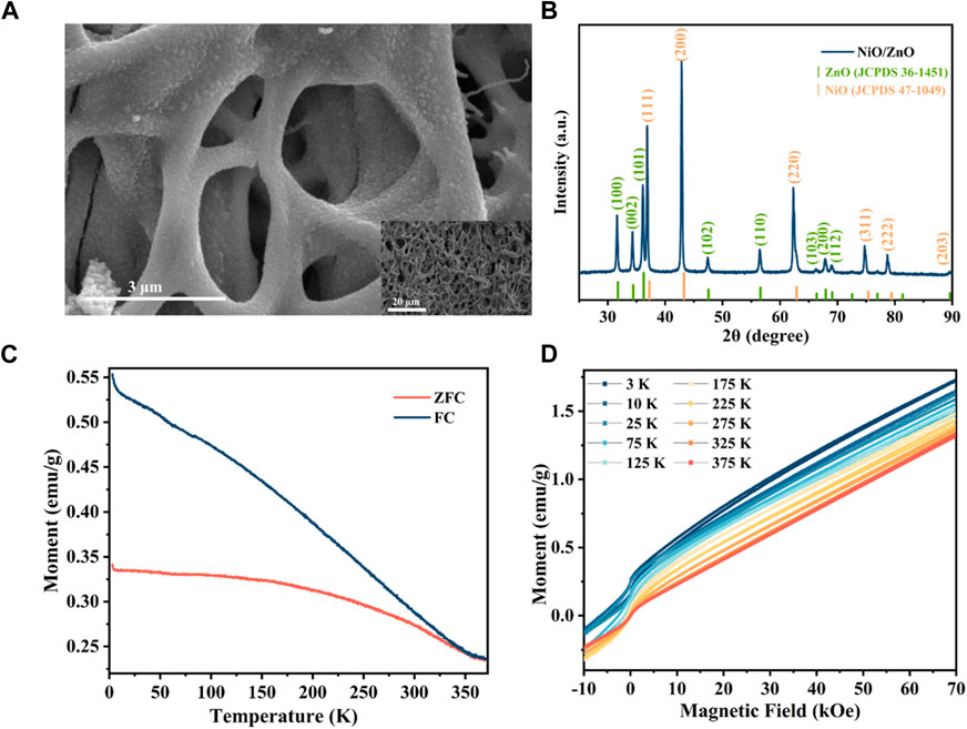
Figure 2. (A) SEM image, (B) XRD pattern, (C) M-T curves measured in an applied magnetic field of 1,000 Oe, (D) M-H curves of the NiO/ZnO heterostructures.
Doping can introduce defects that affect the magnetic properties of the materials. After doping antiferromagnetic NiO [Supplementary Figures S3A, B (Supporting Information)] with non-magnetic ZnO (Supplementary Figures S3A), the magnetization-temperature (M-T) curve (Figure 2C) shows a significant difference between the ZFC and FC curves, with a clear bifurcation between them. As the temperature decreases before the bifurcation point, the difference between the two curves becomes more pronounced, indicating that the composite micro-nanostructures exhibit a spin glass state. The interaction between NiO and ZnO alters the material’s magnetism (Supplementary Figure S4). Additionally, hysteresis loops of the material at different temperatures were measured (Figure 2D), revealing enhanced ferromagnetic properties at lower temperatures, accompanied by increased magnetization in zero magnetic field.
The resistance of NiO/ZnO heterostructures in varying magnetic fields was measured (Figure 3). The green dashed line represents the applied magnetic field. It was observed that applying or removing an external magnetic field resulted in a peak in the resistance. The magnetoresistance (MR), defined as the change in resistance relative to the resistance under zero magnetic field (R₀), is expressed as Equation 1:
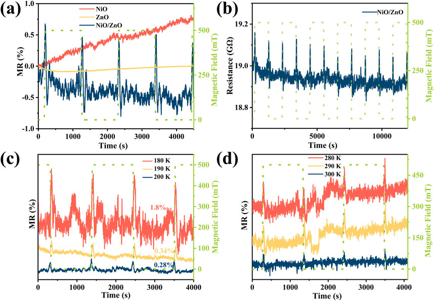
Figure 3. (A) Resistance spikes tests in same magnetic fields were conducted at 300 K for NiO, ZnO, and NiO/ZnO; (B) The stability of this spikes for NiO/ZnO heterostructures; Resistance spikes of (C) NiO micro/nanostructures and (D) NiO/ZnO heterostructures at different temperatures.
This study investigated the maximum resistance variation in a magnetic field (RH), with respect to the resistance under zero magnetic field (R₀). The variation of MR with time is shown in Figure 3, where the y-axis represents MR. The change in sample conductivity continued to decrease even after the magnetic field stopped increasing, possibly due to the long relaxation time of the spin glass state. The magnetic relaxation time for paramagnetic materials (the time from the start to the completion of magnetization) is almost negligible, whereas for spin glasses, it can range from minutes to hours and increases with decreasing temperature, consistent with the relationship between temperature and magnetism [38].
Resistance spikes tests in varying magnetic fields were conducted at room temperature for NiO, ZnO, and NiO/ZnO micro/nanostructures. Significant spikes were observed only in the NiO/ZnO heterostructures at room temperature (Figure 3A), indicating the formation of a heterostructure rather than a simple composite. The heterojunction structure likely extends the observable effect to higher temperatures due to longer relaxation times and easier excitation of electron-hole pairs brought about by the heterojunction structure [39]. Extended testing showed that the composite micro-nanostructures maintained a stable response over a longer period (Figure 3B), while ZnO and NiO exhibited no response under the corresponding magnetic field (Supplementary Figure S5).
Lowering the temperature revealed resistance spikes in the NiO sample at 200 K, 190 K, and 180 K, with MR values of 0.28%, 0.34%, and 1.8%, respectively (Figure 3C). In contrast, ZnO micro-nanostructures did not exhibit resistance spikes in a magnetic field at any temperature. However, the NiO/ZnO composite material still showed magnetoresistance spikes at 290 K and 280 K, with MR values of 5.2% and 10.7%, respectively (Figure 3D). These results align with those of NiO micro/nanostructures, indicating that resistance spikes increase as temperature decreases, albeit with reduced stability. The incorporation of ZnO extends the operational temperature range and enhances the magnetic response of the composite material due to its temperature-dependent magnetic properties. Notably, the composite exhibits room-temperature ferromagnetism with significant magnetic response, which becomes more pronounced at lower temperatures.
The impact of magnetic field orientation and strength was investigated to understand their effects on NiO/ZnO heterostructures. Tests were conducted in different magnetic field directions, revealing that applying a magnetic field in the opposite direction slightly increased resistance spikes (Figure 4A). Furthermore, varying magnetic field magnitudes were tested, showing that higher magnetic field strengths led to increased peak magnetoresistance spikes and broader peaks, indicating enhanced resistance spikes (Figure 4B).
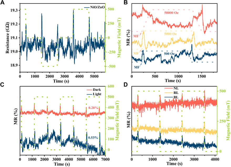
Figure 4. Resistance spikes of NiO/ZnO heterostructures at (A) the opposite magnetic field direction; (B) different magnetic field strengths. Resistance spikes of (C) NiO sample and (D) NiO/ZnO heterostructures at different light illustration conditions.
Next, a 450 nm blue laser was applied to induce photoexcitation in the samples, particularly affecting NiO. Figure 4C shows that exposure to light increased resistance spikes from 0.28% without light to 0.53% with light. Interestingly, under light-induced spikes, the presence of a magnetic field exacerbated this effect.
Additionally, Figure 4D demonstrates sustained photoelectric spikes in the sample, with a conductivity change of approximately 10%. Even after continuous exposure to light for one hundred seconds, the sample’s photoconductivity remained stable and unsaturated, indicating a long lifetime of photo-generated charge carriers. This stability suggests that the composite material, likely due to its defects and oxygen vacancies, is affected by light-induced changes in internal spin polarization, a phenomenon widely reported in literature [40–42].
Control experiments conducted under red light (RL), blue light (BL) and in the absence of light (no light, NL) confirmed significant changes in NiO/ZnO heterostructures even without light, suggesting a competitive effect between the heterojunction structure and light exposure (Figure 4D). The influence of magnetic field on oxygen vacancies could also contribute to observed resistance spikes [43].
However, we performed Electron Paramagnetic Resonance (EPR) tests (Supplementary Figure S6) on the samples to detect oxygen vacancies. The results showed that only ZnO and NiO/ZnO micro/nanostructures exhibited characteristic signals of oxygen vacancies, while NiO sample did not have oxygen vacancies. Therefore, the intensified resistance spike under illumination is not attributed to the effect of oxygen vacancies. Compared to NiO, the photoelectric spike of NiO/ZnO heterostructures increased by approximately 34.7%. We attribute this enhanced spike to the coupling effect between the heterojunction and the magnetic field.
3.2 Further discussion: possible mechanism
NiO/ZnO heterostructures exhibit a network structure that generates an induced current in a varying magnetic field (Supplementary Figure S7). Furthermore, the NiO/ZnO heterostructures form a built-in electric field, causing orderly movement of charges (Figure 5A). The induced current appears in the built-in electric field (Figure 5B), causing disturbances that lead to disordered movement of the previously orderly charges, increasing the probability of collision scattering among the charges, thereby causing resistance spikes.
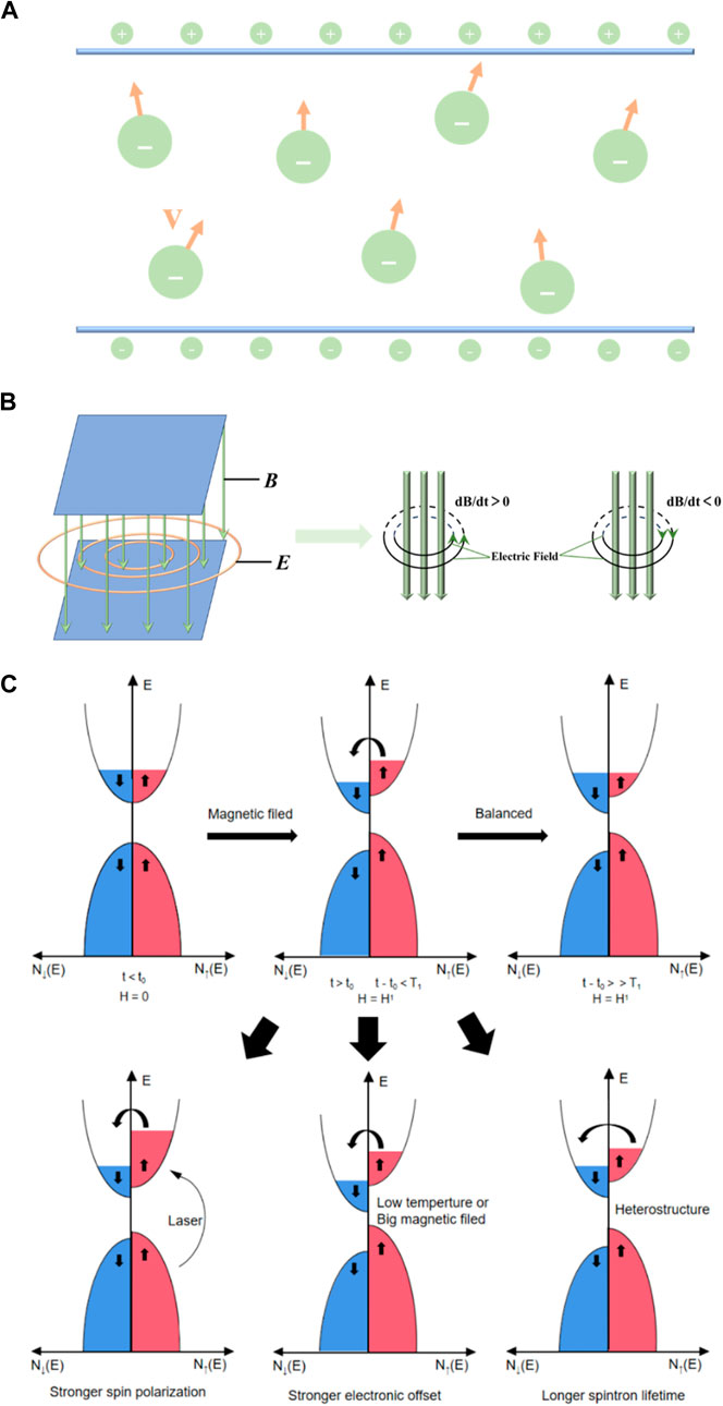
Figure 5. Schematic illustrations of the possible mechanism of resistance spikes phenomenon: (A) charge movement in the heterojunction; (B) electromagnetic induction of the heterojunction in a varying magnetic field; (C) electron spins.
At lower temperatures, resistance typically increases, whereas illumination tends to decrease resistance. Interestingly, both factors enhance resistance spikes, suggesting a dissociation between resistance spikes and absolute resistance values. From the perspective of the electron spin, the rearrangement of electron spin and magnetization directions within NiO/ZnO heterostructures occurs during changes in magnetic fields (Figure 5C). One-dimensional semiconductor nanowires and a spin glass state can prolong spin lifetimes [38, 44]. Lower temperatures enhance material magnetization, while monochromatic laser excitation polarizes electrons, increasing scattering rates. Electron scattering rates depend on the alignment between electron spins and material magnetization directions: when aligned, electron passage through the magnetic layer is facilitated (low impedance); when opposite, electron passage is hindered (high impedance). As electron spins realign with material magnetization post-magnetic field change, resistance returns to pre-magnetic field levels, marking the end of resistance spikes.
The synergistic effect of electron spins and heterojunctions in the magnetic field collectively causes the resistance spikes of the NiO/ZnO heterostructures. The above mechanisms challenge the conventional theory linking resistance spikes to absolute resistance values and emphasize the role of electron spin dynamics, particularly under spin glass states with response times potentially extending to hundreds of seconds.
4 Conclusion
The NiO/ZnO heterostructures were prepared by electrospinning and calcination methods, and their resistance spikes in a magnetic field were measured. These spikes are not only related to the magnetism of the material but also show a greater response to temperature and light illustration compared to pure NiO or ZnO micro/nanostructures. The study revealed that resistance spikes may be due to the disruption of the equilibrium state between heterojunctions or electron spins. This research contributes to understanding the behavior of magnetic heterostructures in magnetic field conditions and holds great potential for applications such as temperature, magnetic field, and light detectors. This work promotes the development of new magnetic electronic devices and advances the progress of information processing and storage technologies.
Data availability statement
The original contributions presented in the study are included in the article/Supplementary Material, further inquiries can be directed to the corresponding author.
Author contributions
Y-ZS: Writing–review and editing, Data curation, Writing–original draft. L-PQ: Data curation, Writing–original draft. S-LG: Conceptualization, Writing–review and editing. S-ZC: Methodology, Writing–review and editing. S-JW: Formal Analysis, Writing–review and editing. W-PH: Methodology, Writing–review and editing. JZ: Formal Analysis, Writing–review and editing. Y-ZL: Funding acquisition, Writing–review and editing.
Funding
The author(s) declare that financial support was received for the research, authorship, and/or publication of this article. This work was supported by the National Natural Science Foundation of China (52273077), and the State Key Laboratory of Bio-Fibers and Eco-Textiles, Qingdao University (ZDKT202108).
Conflict of interest
The authors declare that the research was conducted in the absence of any commercial or financial relationships that could be construed as a potential conflict of interest.
Generative AI statement
The author(s) declare that no Generative AI was used in the creation of this manuscript.
Publisher’s note
All claims expressed in this article are solely those of the authors and do not necessarily represent those of their affiliated organizations, or those of the publisher, the editors and the reviewers. Any product that may be evaluated in this article, or claim that may be made by its manufacturer, is not guaranteed or endorsed by the publisher.
Supplementary material
The Supplementary Material for this article can be found online at: https://www.frontiersin.org/articles/10.3389/fphy.2024.1524692/full#supplementary-material
References
1. Wu Y, Li T, Ren X, Fu Y, Zhang H, Feng X, et al. Magnetic field assisted α-Fe2O3/Zn1−xFexO heterojunctions for accelerating antiviral agents degradation under visible-light. J Environ Chem Eng (2022) 10:106990. doi:10.1016/j.jece.2021.106990
2. García de Arquer FP, Talapin DV, Klimov VI, Arakawa Y, Bayer M, Sargent EH. Semiconductor quantum dots: technological progress and future challenges. Science (2021) 373:eaaz8541. doi:10.1126/science.aaz8541
3. Liu W, Zhang H, Shi J-a., Wang Z, Song C, Wang X, et al. A room-temperature magnetic semiconductor from a ferromagnetic metallic glass. Nat Commun (2016) 7:13497. doi:10.1038/ncomms13497
4. Sato N, Xue F, White RM, Bi C, Wang SX. Two-terminal spin–orbit torque magnetoresistive random access memory. Nat Elect (2018) 1:508–11. doi:10.1038/s41928-018-0131-z
5. Shinya H, Fukushima T, Sato K, Ohya S, Katayama-Yoshida H. Theoretical study on the origin of anomalous temperature-dependent electric resistivity of ferromagnetic semiconductor. APL Mater (2023) 11:111114. doi:10.1063/5.0165352
6. Chen N, Fang K, Zhang H, Zhang Y, Liu W, Yao K, et al. Amorphous magnetic semiconductors with Curie temperatures above room temperature. J Semiconductors (2019) 40:081510. doi:10.1088/1674-4926/40/8/081510
7. Li W, Cheng G, Sun M, Wu Z, Liu G, Su D, et al. C-CoP hollow microporous nanocages based on phosphating regulation: a high-performance bifunctional electrocatalyst for overall water splitting. Nanoscale (2019) 11:17084–92. doi:10.1039/c9nr05061b
8. Sato T, Hori A. Aging behavior of semiconductor spin-glass under photo illumination. J Magnetism Magn Mater (2004) 272-276:1337–9. doi:10.1016/j.jmmm.2003.12.593
9. Zhang Z, Ning Y, Fang X. From nanofibers to ordered ZnO/NiO heterojunction arrays for self-powered and transparent UV photodetectors. J Mater Chem C (2019) 7:223–9. doi:10.1039/c8tc05877f
10. You W, Zheng B, Xu Z, Jiang Y, Zhu C, Zheng W, et al. Strong interfacial coupling in vertical WSe2/WS2 heterostructure for high performance photodetection. Appl Phys Lett (2022) 120:181108. doi:10.1063/5.0082101
11. Wang XL, Du Y, Dou SX, Zhang C. Room temperature giant and linear magnetoresistance in topological insulator Bi2Te3 nanosheets. Phys Rev Lett (2012) 108:266806. doi:10.1103/physrevlett.108.266806
12. Liu N, Du P, Zhou P, Tanguturi RG, Qi Y, Zhang T. Magnetoelectric coupling in CoFe2O4-Pb(Zr0.2Ti0.8)O3 coaxial nanofibers. J Am Ceram Soc (2021) 104:948–54. doi:10.1111/jace.17494
13. Liu J, Wang L, Niu M, Jiang R, Liu Y, Xu D, et al. Enhanced magnetoelectric coupling characteristics of Mn2O3-modified BiFeO3-based ceramics. J Magnetism Magn Mater (2021) 527:167777. doi:10.1016/j.jmmm.2021.167777
14. Dagotto E, Hotta T, Moreo A. Colossal magnetoresistant materials: the key role of phase separation. Phys Rep (2001) 344:1–153. doi:10.1016/s0370-1573(00)00121-6
15. Cai J, Zhao J, Gao X, Ma W, Meng D, Zhang H, et al. Magnetic field tuning ionic current generated by chiromagnetic nanofilms. ACS Nano (2022) 16:11066–75. doi:10.1021/acsnano.2c03778
16. Fasasi TA, Apicella V, Li D, Ruotolo A. Photoinduced Hall effect for low-temperature magnetic sensing. IEEE Magnetics Lett (2019) 10:1–4. doi:10.1109/lmag.2019.2938722
17. Fasasi TA, Ruotolo A, Zhao XW, Leung CW, Lin KW. Photo-induced anomalous Hall effect in nickel thin films. J Magnetism Magn Mater (2019) 485:82–4. doi:10.1016/j.jmmm.2019.04.075
18. Wang X, Sun X, Cui S, Yang Q, Zhai T, Zhao J, et al. Physical investigations on bias-free, photo-induced Hall sensors based on Pt/GaAs and Pt/Si Schottky junctions. Sensors (2021) 21:3009. doi:10.3390/s21093009
19. Zhou ZB, Zhang XW, Guo YL, Zhang YH, Niu XH, Ma L, et al. Ultralong lifetime for fully photogenerated spin-polarized current in two-dimensional ferromagnetic/nonmagnetic semiconductor heterostructures. Phys Rev B (2021) 103:245411. doi:10.1103/physrevb.103.245411
20. Guo K, Zhang R, Fu Z, Zhang L, Wang X, Deng C. Regulation of photovoltaic response in ZSO-based multiferroic BFCO/BFCNT heterojunction photoelectrodes via magnetization and polarization. ACS Appl Mater and Inter (2021) 13:35657–63. doi:10.1021/acsami.1c07534
21. Hu J, Zhang Q, Zhou P, Mei C, Huang X, Dong A, et al. Sensitive photoelectric response to magnetic field in p-type silicon-based structures. IEEE Photon Tech Lett (2017) 29:1848–51. doi:10.1109/lpt.2017.2753405
22. Pan D-F, Chen G-Y, Bi G-F, Zhang H, Liu J-M, Wang G-H, et al. Tuning the photovoltaic effect of multiferroic CoFe2O4/Pb(Zr, Ti)O3 composite films by magnetic fields. Appl Phys Lett (2016) 108:222902. doi:10.1063/1.4953154
23. Wang S, Wang W, Zou L, Zhang X, Cai J, Sun Z, et al. Magnetic tuning of the photovoltaic effect in silicon-based Schottky junctions. Adv Mater (2014) 26:8059–64. doi:10.1002/adma.201403868
24. Zhou P, Gan Z, Huang X, Mei C, Xia Y, Wang H. Size-dependent magnetic tuning of lateral photovoltaic effect in nonmagnetic Si-based Schottky junctions. Scientific Rep (2017) 7:46377. doi:10.1038/srep46377
25. Zhao G, Ding J, Zhou F, Chen X, Wei L, Gao Q, et al. Construction of a visible-light-driven magnetic dual Z-scheme BiVO4/g-C3N4/NiFe2O4 photocatalyst for effective removal of ofloxacin: mechanisms and degradation pathway. Chem Eng J (2021) 405:126704. doi:10.1016/j.cej.2020.126704
26. Xian Y, Zheng N, Du A. Magnetic properties of XXZ Heisenberg antiferromagnetic and ferromagnetic core-shell nanowires. J Appl Phys (2018) 124:184304. doi:10.1063/1.5057381
27. Semenov YG, Xu X, Kim KW. Thermal fluctuations in antiferromagnetic nanostructures. J Magnetism Magn Mater (2019) 489:165457. doi:10.1016/j.jmmm.2019.165457
28. Das AK, Srinivasan A. Evidence of oxygen defect induced ferromagnetism in heat treated electrospun ZnO nanowires. J Magnetism Magn Mater (2016) 404:190–6. doi:10.1016/j.jmmm.2015.12.032
29. Siddique MN, Tripathi P. Lattice defects formulated ferromagnetism in nonmagnetic La (III) ion doped NiO nanostructures: role of oxygen vacancy. J Alloys Comp (2020) 825:154071. doi:10.1016/j.jallcom.2020.154071
30. Kaur N, Zappa D, Ferroni M, Poli N, Campanini M, Negrea R, et al. Branch-like NiO/ZnO heterostructures for VOC sensing. Sensors Actuators B: Chem (2018) 262:477–85. doi:10.1016/j.snb.2018.02.042
31. Qiao L, Wang X, Qiao L, Sun X, Li X, Zheng Y, et al. Single electrospun porous NiO–ZnO hybrid nanofibers as anode materials for advanced lithium-ion batteries. Nanoscale (2013) 5:3037–42. doi:10.1039/c3nr34103h
32. Chen Z, Dedova T, Spalatu N, Maticiuc N, Rusu M, Katerski A, et al. ZnO/NiO heterostructures with enhanced photocatalytic activity obtained by ultrasonic spraying of a NiO shell onto ZnO nanorods. Colloids Surf A: Physicochemical Eng Aspects (2022) 648:129366. doi:10.1016/j.colsurfa.2022.129366
33. Trotsenko O, Tokarev A, Gruzd A, Enright T, Minko S. Magnetic field assisted assembly of highly ordered percolated nanostructures and their application for transparent conductive thin films. Nanoscale (2015) 7:7155–61. doi:10.1039/c5nr00154d
34. Jia Y, Yang C, Chen X, Xue W, Hutchins-Crawford HJ, Yu Q, et al. A review on electrospun magnetic nanomaterials: methods, properties and applications. J Mater Chem C (2021) 9:9042–82. doi:10.1039/d1tc01477c
35. Li G-Y, Zhang H-D, Li Z-J, Gao H, Wang N, Li R, et al. Enhanced simulated solar sono-photocatalytic performance and antibacterial activities of ZnO/NiO heterojunction nanofibrous membranes. Ceramics Int (2022) 48:9442–9. doi:10.1016/j.ceramint.2021.12.141
36. Augustine P, Kumawat KL, Singh DK, Krupanidhi SB, Nanda KK. MoS2/SnO2 heterojunction-based self-powered photodetector. Appl Phys Lett (2022) 120:181106. doi:10.1063/5.0087652
37. Yang J, Hu X, Kong X, Jia P, Ji D, Quan D, et al. Photo-induced ultrafast active ion transport through graphene oxide membranes. Nat Commun (2019) 10:1171. doi:10.1038/s41467-019-09178-x
38. Hsu J-H, Lee JT, Chang C-R, Lin MT. Long magnetic relaxation time of Fe–Bi spin-glass system. J Magnetism Magn Mater (2001) 226-230:502–4. doi:10.1016/s0304-8853(00)00988-4
39. Wu W-Q, Chen D, Li F, Pascoe AR, Cheng Y-B, Caruso RA. Integrated planar and bulk dual heterojunctions capable of efficient electron and hole extraction for perovskite solar cells with >17% efficiency. Nano Energy (2017) 32:187–94. doi:10.1016/j.nanoen.2016.12.029
40. Li G, Yang W, Gao S, Shen Q, Xue J, Chen K, et al. Creation of rich oxygen vacancies in bismuth molybdate nanosheets to boost the photocatalytic nitrogen fixation performance under visible light illumination. Chem Eng J (2021) 404:127115. doi:10.1016/j.cej.2020.127115
41. Zheng S, Duley WW, Peng P, Norman Zhou Y. Engineering intrinsic defects in CuO NWs through laser irradiation: oxygen vs copper vacancies. Appl Surf Sci (2024) 642:158630. doi:10.1016/j.apsusc.2023.158630
42. Fujino H, Koh S, Iba S, Fujimoto T, Kawaguchi H. Circularly polarized lasing in a (110)-oriented quantum well vertical-cavity surface-emitting laser under optical spin injection. Appl Phys Lett (2009) 94:131108. doi:10.1063/1.3112576
43. Deng L, Hu H, Wang Y, Wu C, He H, Li J, et al. Surface plasma treatment reduces oxygen vacancies defects states to control photogenerated carriers transportation for enhanced self-powered deep UV photoelectric characteristics. Appl Surf Sci (2022) 604:154459. doi:10.1016/j.apsusc.2022.154459
Keywords: electrospinning, heterostructures, magnetoresistance, electromagnetic induction, resistance spikes
Citation: Sun Y-Z, Qiu L-P, Gao S-L, Cao S-Z, Wang S-J, Han W-P, Zhang J and Long Y-Z (2025) Resistance spikes of NiO/ZnO heterostructures in magnetic field. Front. Phys. 12:1524692. doi: 10.3389/fphy.2024.1524692
Received: 11 November 2024; Accepted: 30 December 2024;
Published: 17 January 2025.
Edited by:
Xichao Zhang, Waseda University, JapanReviewed by:
Su Kong Chong, University of California, Los Angeles, United StatesHailan Luo, University of California, Berkeley, United States
Copyright © 2025 Sun, Qiu, Gao, Cao, Wang, Han, Zhang and Long. This is an open-access article distributed under the terms of the Creative Commons Attribution License (CC BY). The use, distribution or reproduction in other forums is permitted, provided the original author(s) and the copyright owner(s) are credited and that the original publication in this journal is cited, in accordance with accepted academic practice. No use, distribution or reproduction is permitted which does not comply with these terms.
*Correspondence: Yun-Ze Long, eXVuemUubG9uZ0AxNjMuY29t, eXVuemUubG9uZ0BxZHUuZWR1LmNu
†These authors have contributed equally to this work