- 1The 41st Institute of China Electronics Technology Group Corporation, Qingdao, China
- 2National Opto-Electronic Primary Metrology Laboratory, Qingdao, China
- 3School of Information Science and Engineering, Shandong University, Qingdao, China
- 4College of Optics and Electronic Science and Technology, China Jiliang University, Hangzhou, China
This paper presents the design of a high-efficiency spot size converter (SSC) for photonic crystal fiber (PCF) to silicon-based waveguides, utilizing composite optical waveguide structures. The SSC is composed of a series of waveguide cores, with one core progressively widening to enable all cores to collectively serve as a composite input port, while the broader core functions as the output port. Simulation results reveal that the proposed design efficiently facilitates mode and energy transfer between the waveguide and the PCF, achieving a coupling efficiency of up to 93.99% over a length of 66 μm. Additionally, the SSC exhibits polarization insensitivity, with the high circularity of the output beam enhancing vertical alignment tolerance, and maintaining excellent performance over a wide wavelength range. In sum, this SSC demonstrates excellent coupling efficiency and holds significant promise for applications in optical communication systems and optical integrated circuit systems.
1 Introduction
With the increasing demand for ultra-compact and low-cost photonic devices, the development of silicon photonics platforms has garnered widespread attention [1,2]. Silicon-based waveguides, owing to their high integration density, mature fabrication processes, and compatibility with complementary metal-oxide-semiconductor (CMOS) manufacturing technologies, have emerged as the preferred platform for constructing large-scale photonic integrated circuits [3]. This technology is particularly well-suited for high-volume data communication and telecommunication optical products. Photonic crystal fibers present a compelling solution for achieving ultra-high-speed data transmission, thanks to their tunable dispersion characteristics and elevated nonlinearity coefficients [4,5]. Particularly notable are hollow-core photonic crystal fibers, which feature unique air or gas core structures that significantly reduce material absorption and scattering losses [6–8]. These structures also substantially enhance nonlinear interactions and spectral absorption properties within the fiber. Consequently, hollow-core photonic crystal fibers demonstrate significant application potential in frequency-stabilized laser systems based on molecular absorption, distributed fiber optic sensing, femtosecond lasers, and ultra-short pulse transmission [9–12]. However, achieving high efficiency coupling between optical fibers and silicon-based waveguides on the silicon photonics platform remains one of the primary challenges in this field [13, 14]. Due to the mismatch in the transverse dimensions of the waveguides, single-mode silicon waveguides often encounter significant losses when coupling with optical fibers.
Currently, several approaches have been proposed to address the coupling between fibers and silicon-based waveguides, including direct coupling, grating coupling, prism coupling, and waveguide overlay coupling methods [15, 16]. For instance, lens couplers utilize micro-lenses to precisely control the focusing and collimation of light, while tapered couplers reduce mode mismatch by gradually varying the waveguide width [17]. Although grating couplers offer a large mode profile, their limited bandwidth and polarization dependence restrict their use in broadband optical communications [18, 19]. Edge couplers offer broad bandwidth and low polarization-dependent loss, but traditional inverse taper edge couplers, with a typical mode size of around 3 μm, often involve pairing with lensed fibers [20]. Since precise alignment between the lens and the coupler is necessary, the complexity of packaging increases. Reference [21] introduced a low-loss, broadband, silicon nitride-assisted edge coupler optimized for TE polarization, designed for coupling between silicon wire waveguides and high numerical aperture fibers. This approach achieved a coupling loss of only 0.35 dB at 1,570 nm, with a 1 dB bandwidth of 95 nm. However, these methods still face certain limitations in terms of structural complexity, compatibility with fabrication processes, and coupling bandwidth.
Despite significant progress in addressing coupling issues between traditional optical fibers and waveguides, the coupling between silicon-based waveguides and photonic crystal fibers (PCFs) still requires further investigation. In recent years, composite waveguide structure based spot size converter (SSC) has garnered significant attention due to their structural simplicity, excellent compatibility, and ease of integration [22]. This kind of SSC achieves effective mode matching with fibers by precisely controlling the dimensions and stacking structure of the waveguides, which significantly enhances coupling efficiency. For example, a study presented a vertical interlayer coupler that employs a nonlinear taper structure between two silicon layers to facilitate efficient coupling [23]. Simulation results show that within the wavelength range of 1,500 nm–1650 nm, this structure can achieve coupling efficiencies exceeding 90%, with crosstalk reduced to below −50 dB by using multimode waveguides at the intersections. This highlights the considerable potential of vertical interlayer couplers for miniaturizing and integrating photonic chips with high density. Although research has significantly improved coupler performance, further optimization of coupling efficiency, reduction in losses, and bandwidth expansion remain crucial areas of study for practical applications.
This paper introduces an innovative design for a composite optical waveguide based SSC. The converter consists of a series of waveguide cores, with the main core widening gradually through a tapering structure to form a composite input port, while the widest core serves as the output port. All waveguide cores are made from Si3N4 material, leveraging its excellent optical properties and chemical stability to ensure high device performance. The design method can also employ Si3N4 layers as, etch stop layers to ensure precise control over the waveguide geometry. This innovative design achieves a high level of efficiency in mode and energy transfer between optical waveguides and photonic crystal fibers. Simulations of the device structure using the eigenmode expansion method validate the effectiveness of the design, demonstrating a coupling efficiency of up to 92.73%. Moreover, the SSC exhibits polarization insensitivity. Compared to traditional trident structures, its high circularity enhances alignment tolerance in the vertical direction. Finally, the universality of the SSC is confirmed across a wide wavelength range. The results demonstrate that the designed SSC exhibited sustained high coupling efficiency throughout the entire spectrum under investigation, peaking at 93.99%, with oscillations remaining within a 2.6% margin. These attributes significantly improve its applicability and flexibility across various optical systems. With the ongoing advancements in photonic integrated circuit technology, the SSC proposed in this paper is poised to play a pivotal role in fields such as optical communication, quantum information processing, and bio-photonics, providing a technical foundation for the development of more compact and efficient optical systems. Additionally, the design approach presented in this work may serve as a reference for the development of other types of waveguides coupling devices.
2 Theory and design
Hollow-core photonic crystal fibers (HC-PCFs) are characterized by their periodic arrangement of air holes across the cross-section [24]. The arrangement, size, and structure of these air holes, as well as the core region of the fiber, collectively determine light guiding properties [25]. Typically, PCF designs include a region that disrupts the periodicity, which can be a single large air hole or a series of missing air holes. This design allows for the formation of specific optical modes within the core of the fiber, enabling effective guidance and control of light. HC-PCFs offer a range of distinctive advantages compared to traditional optical fibers, which include extremely low nonlinear coefficients, adjustable dispersion characteristics, high damage thresholds, and excellent beam quality [26]. These benefits arise from the precise structure and arrangement of the air holes, which can be highly customized in terms of diameter, shape, and spacing to optimize the transmission properties of the fiber. For instance, by adjusting the size and spacing of the air holes, precise control over the dispersion of the fiber can be achieved, allowing for the tailoring of optical properties to meet specific application needs [27]. Additionally, the low nonlinear characteristics of HC-PCFs make them exceptional for high-power transmission and nonlinear optical applications, while their high damage threshold and superior beam quality provide advantages in high-precision optical applications [28]. In this work, the cross-section of the employed HC-PCF is shown in Figure 1A.
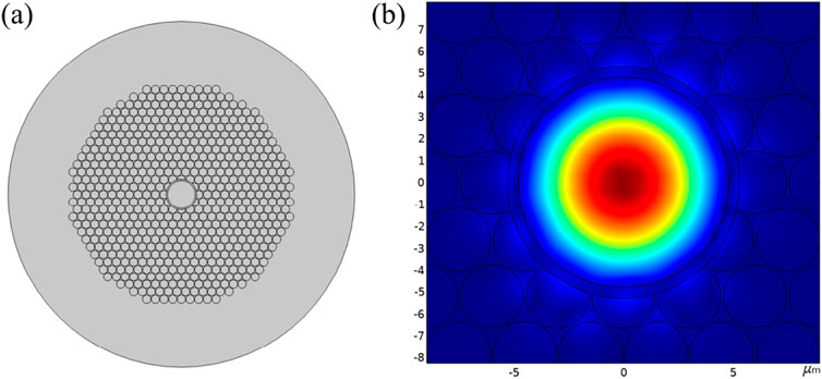
Figure 1. (A) The cross-section of the PCF structure, (B) the electrical field of fiber fundamental mode.
The radius of the cladding air holes is 1.44 μm, the distance between the centers of two adjacent air holes is 3 μm, the radius of the central hollow core is 4.8 μm, and the wall thickness of the core is 0.492 μm. Subsequently, full-vector finite element method (FEM) simulations are conducted to solve the modes of this fiber. The software used for PCF simulation is COMSOL. The optical field profile at a typical communication wavelength (λ) of 1.54 μm is shown in Figure 1B. The imaginary part of the effective refractive index (neff) is 3.294723 × 10⁻¹⁰. Using Equation 1, the confinement loss (Lc) of this fiber is 0.0117 dB/m, which meets the loss requirements for communication fibers [29].
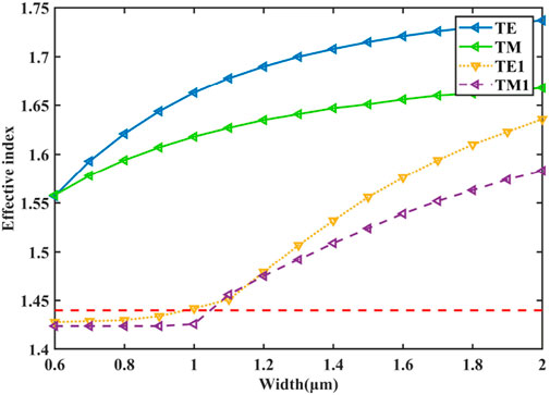
The waveguide width influences both the lateral electric field distribution and the value of the effective refractive index in Si3N4 waveguides [30]. By analyzing the effective refractive index of the waveguide, the mode characteristics and transmission properties of the waveguide can be determined. During the waveguide simulation, the cladding refractive index is set as 1.44 and the core refractive index is set as 1.97. The software used in the waveguide simulation is Lumerical. Narrower waveguides exhibit lower effective refractive indices, while an increase in width generally leads to an increase in the effective refractive index, affecting the propagation speed of light and the mode distribution. Therefore, selecting the appropriate waveguide width requires balancing support for specific modes with considerations of loss and coupling efficiency. In this work, a Si3N4 waveguide with a thickness of 0.25 μm is discussed, and the characteristics of its effective refractive index as a function of waveguide width are analyzed. Figure 2 illustrates the variation in neff of the Si3N4 waveguide across different widths. The red dotted line in the figure indicates the refractive index of the cladding during the simulation. The effective refractive index of the mode propagating in the waveguide is greater than this value. The width of the waveguide determines the supported optical modes. Narrow waveguides typically support only a limited number of modes, such as TE and TM modes. As the width increases, more propagation modes may emerge. The selected waveguide structure in this work, with a width of 0.8 μm, effectively supports the transmission of TE and TM modes while suppressing higher-order modes. This is crucial for ensuring stable signal transmission and efficient coupling.
Several common SSC designs, including grating couplers and edge taper waveguide couplers, have been previously discussed. Each of these designs offers specific advantages in practical applications but also presents certain limitations. For instance, grating couplers exhibit polarization dependence and higher insertion loss, while edge taper waveguide couplers face challenges related to precise alignment. To address these issues, this paper proposes a SSC design based on composite waveguide structures. The aim is to achieve more efficient optical coupling by optimizing the waveguide design, thereby reducing mode mismatch and transmission loss, and ultimately enhancing the overall system performance. The designed SSC is composed of multiple waveguide cores that are coupled through evanescent waves. One of the cores is designed with a larger size to serve as the output port, while the other cores function as input ports. The width of the waveguide cores gradually varies from the input to the output to optimize optical coupling and transmission efficiency. The coupling efficiency is quantitatively analyzed by calculating the overlap integral between the modes of the PCF and the output light spot of the coupler. The mode overlap (η) is given by Equation 2 [31]:
where
After parameter adjustments and optimization, the SSC consists of three short tapered waveguide cores and one long tapered waveguide core, as illustrated in Figure 3. The refractive index of silicon nitride in the simulation is 2.01. To further reduce the size of the device, the long tapered waveguide core is designed in multiple segments. This approach minimizes optical loss while reducing the size of the converter to 66 μm. In this structure, the width of the end-face waveguides and the spacing between them affect the final coupling efficiency. Therefore, taking TE mode as an example, the effects of the width of end-face waveguides and the spacing between end-face waveguides on the coupling efficiency are calculated. The calculation results are shown in Figure 4. It can be seen from the figure that the coupling efficiency increases with the decrease in the end width of the waveguide, but considering the actual process level and the difficulty of fabrication, the waveguide width is set as 200 nm. And the coupling efficiency increases with the increase of the spacing between waveguides. However, when the spacing is too large, the light cannot spread to all waveguides at the end face, leading to a large difference between the size of the end face spot and the optical fiber spot, and the coupling efficiency will drop sharply. Therefore, the spacing between waveguides is set as 2 μm. The specific dimensional parameters are listed in Table 1.

Figure 3. (A) The proposed SSC structure, schematic diagram of waveguide geometric parameters (B) XY plane and (C) XZ plane.
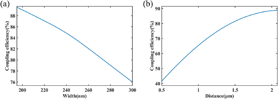
Figure 4. Changes in coupling efficiency due to size changes: (A) end-face waveguide width, (B) waveguide spacing.
3 Results and discussion
3.1 Coupling efficiency
Next, simulation is conducted on the model to evaluate its coupling performance. Figure 5 shows the mode spot image at the end face of the SSC. The letter numbers in Figure 5 correspond to the slice points in Figure 3C. The results indicate that the mode spot significantly expands under the action of this structure. This phenomenon demonstrates that the SSC effectively facilitates the conversion between different mode sizes. Specifically, the design of the structure allows for the conversion of the waveguide mode sizes smaller than 1 μm to fiber mode sizes larger than 5 μm, which is crucial for coupling with fibers of varying sizes. This expansion of mode size not only enhances the compatibility with optical fibers but also optimizes the transmission efficiency of optical signals.
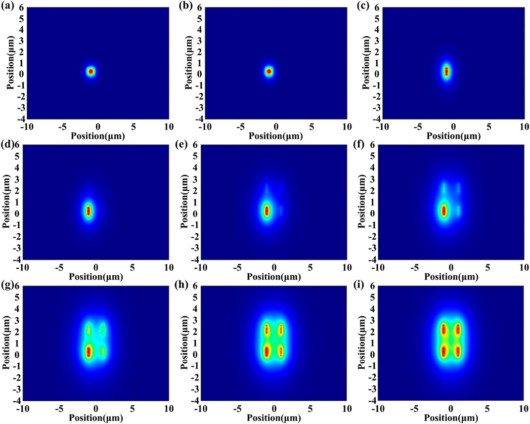
Figure 5. The widening process of the light spot from the silicon waveguide to the fiber through the SSC. (A-I) correspond to the section positions in Figure 3C.
Figure 5 demonstrates that the light spot within the waveguide of the SSC progressively enters the PCF after passing through the end face. As the light spot propagates through the SSC, the size undergoes substantial variation. Specifically, the size of the light spot changes according to the geometric configuration of the waveguide array. This variation results from the influence of the waveguide dimensions on the mode distribution of the light. As the light spot approaches the long-tapered waveguide core, the size increasingly conforms to that of the core, ultimately achieving stable transmission within the core.
This process can be explained by the gradual waveguide structure of the SSC. The progressive expansion of the waveguide array allows the mode of the light to transition from a small size mode to a larger size mode, thereby achieving effective mode conversion. This structural design not only optimizes the expansion process of the light but also enhances the efficiency of its transmission. Specially, the introduction of the long-tapered waveguide core further ensures stable transmission and mode matching. This gradient and transition mechanism is a key factor in achieving efficient coupling, effectively reducing losses due to mode mismatch and improving the overall performance of the system. The optical energy transfer process is shown in Figure 6.
Next, the eigenmode expansion method is employed to simulate the designed structure with a wavelength of 1,542 nm, a standard wavelength in optical communication to ensure the practicality and relevance of the results. During the simulation, coupling efficiencies for both TE and TM modes are calculated to assess the polarization dependence of the structure. Since the design of the SSC involves the conversion between different modes, it is essential to verify its polarization insensitivity to ensure its wide applicability in practical applications. The highest coupling efficiency for the TE mode is 89.04%, and for the TM mode is 92.73%. The results indicate that the designed SSC achieves a high coupling efficiency, and changes in polarization state do not affect the performance of the SSC.
3.2 Tolerance analysis
To further investigate the performance of the composite waveguide structure SSC, a tolerance analysis of the waveguide structure is performed. The analysis involves displacing the PCF in both horizontal and vertical directions and calculating the coupling efficiency between the displaced fiber modes and the waveguide modes. The computed data is presented in Figure 7. Note that the data with reverse offset is symmetrical, so only half of the offset analysis data is shown in the figure.
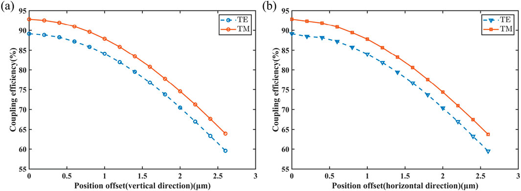
Figure 7. Changes in coupling efficiency due to alignment offset: (A) vertical direction, (B) horizontal direction.
Figure 7 demonstrates that, both vertically and horizontally, the TM mode maintains a tolerance range greater than 4 μm within a 1 dB tolerance level, while the TE mode maintains a tolerance range greater than 3.6 μm at the same level. This indicates that the SSC retains a high coupling efficiency even when the fiber displacement reaches up to 4 μm. Specifically, within a displacement of 2.8 μm, the coupling efficiency for both TE and TM modes remains above 80%, and even within a 4 μm range, the coupling efficiency stays above 70%. These results suggest that the designed SSC exhibits excellent alignment tolerance. In practical applications, this high tolerance performance significantly reduces the need for precise alignment, thereby simplifying the manufacturing and package processes. Additionally, the polarization insensitivity of this SSC further enhances its applicability under various operating conditions.
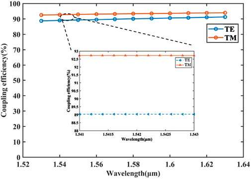
To ensure that the designed structure can be applied across different wavelength bands, the coupling efficiency was further calculated over the wavelength range of 1.53 μm–1.63 μm, as shown in Figure 8. The results indicate that within the investigated wavelength range, the performance of the SSC remains above 88.7%, with absolute fluctuations not exceeding 2.6%. Particularly noteworthy is the achievement of a 93.99% coupling efficiency at a wavelength of 1.63 μm. This demonstrates that the SSC can effectively handle signals across wide wavelength band in practical applications. Specifically, in optical communication systems requiring wide-band operation, this SSC can provide reliable performance support.
4 Conclusion
This paper designs an efficient SSC composed of composite waveguide structures for coupling between PCFs and silicon-based waveguides. The efficient coupling capability of the designed structure is first validated using the eigenmode expansion method. Simulation results indicate that the designed SSC achieves coupling efficiencies of 92.73% and 89.04% for TE and TM modes, respectively, significantly enhancing the coupling performance. The length of the SSC is limited to 66 μm by employing optimized waveguide structure. To further enhance the applicability of the design, tolerance analysis of the SSC is conducted. Results indicate that within a displacement range of 2.8 μm, the coupling efficiency remains above 80%, demonstrating excellent alignment tolerance and suitability for practical alignment requirements. Additionally, to ensure performance across different wavelength bands, coupling efficiency over the wavelength range from 1,530 nm to 1630 nm is analyzed. Results show that the coupling efficiency remains above 88.7% within this range (93.99% at 1.63 μm), with fluctuations not exceeding 2.6%, indicating excellent broadband adaptability. In summary, the SSC efficiently converts between different mode sizes and is suitable for high-efficiency coupling between PCFs and silicon-based waveguides. This SSC not only has broad application potential in the communication field but also provides a solid technical foundation for efficient optical interfaces in future photonic integrated circuits. Its outstanding tolerance performance and wideband stability enhance its significant value and promising prospects for practical applications, particularly in high-precision optical communication systems and advanced photonic integrated circuits.
Data availability statement
The original contributions presented in the study are included in the article/supplementary material, further inquiries can be directed to the corresponding authors.
Author contributions
HL: Conceptualization, Data curation, Formal Analysis, Funding acquisition, Methodology, Project administration, Resources, Software, Writing–original draft, Writing–review and editing. BL: Conceptualization, Data curation, Formal Analysis, Funding acquisition, Investigation, Methodology, Supervision, Writing–original draft, Writing–review and editing. XZ (3rd author): Conceptualization, Data curation, Software, Writing–original draft, Writing–review and editing. LC: Conceptualization, Data curation, Formal Analysis, Software, Writing–original draft. BW: Funding acquisition, Methodology, Project administration, Resources, Supervision, Writing–review and editing. LZ: Conceptualization, Data curation, Software, Writing–original draft. XZ (7th author): Data curation, Validation, Visualization, Writing–original draft. YG: Methodology, Formal Analysis, Writing–review and editing. HW: Project administration, Resources, Supervision, Writing–review and editing.
Funding
The author(s) declare that financial support was received for the research, authorship, and/or publication of this article. This work was supported in part by the National Key R&D Program of China under Grant No: 2023YFF0722400, in part by the National Natural Science Foundation of China under Grant No: U2241218; in part by “Opening Foundation of Key Laboratory of Laser and Infrared System (Shandong University), Ministry of Education”.
Conflict of interest
Authors HL, BL, XZ (3rd author), BW, LZ, XZ (7th author), YG, and HW were employed by The 41st Institute of China Electronics Technology Group Corporation.
The remaining author declares that the research was conducted in the absence of any commercial or financial relationships that could be construed as a potential conflict of interest.
Generative AI statement
The author(s) declare that no Generative AI was used in the creation of this manuscript.
Publisher’s note
All claims expressed in this article are solely those of the authors and do not necessarily represent those of their affiliated organizations, or those of the publisher, the editors and the reviewers. Any product that may be evaluated in this article, or claim that may be made by its manufacturer, is not guaranteed or endorsed by the publisher.
References
1. Rahim A, Spuesens T, Baets R, Bogaerts W. Open-access silicon photonics: current status and emerging initiatives. Proc IEEE (2018) 106(12):2313–30. doi:10.1109/jproc.2018.2878686
2. Siew SY, Li B, Gao F, Zheng HY, Zhang W, Guo P, et al. Review of silicon photonics technology and platform development. J Lightwave Technology (2021) 39(13):4374–89. doi:10.1109/jlt.2021.3066203
3. Chen X, Milosevic MM, Stanković S, Reynolds S, Bucio TD, Li K, et al. The emergence of silicon photonics as a flexible technology platform. Proc IEEE (2018) 106(12):2101–16. doi:10.1109/jproc.2018.2854372
5. Russell PSJ, Hӧlzer P, Chang W, Abdolvand A, Travers JC. Hollow-core photonic crystal fibres for gas-based nonlinear optics. Nat Photon (2014) 8(4):278–86. doi:10.1038/nphoton.2013.312
6. Ni W, Yang C, Luo Y, Xia R, Lu P, Hu DJJ, et al. Recent advancement of anti-resonant hollow-core fibers for sensing applications. Photonics (2021) 8:128. doi:10.3390/photonics8040128
7. Travers JC. Optical solitons in hollow-core fibres. Opt Commun (2024) 555:130191. doi:10.1016/j.optcom.2023.130191
8. Ding H, Hu DJJ, Yu X, Liu X, Zhu Y, Wang G. Review on all-fiber online Raman sensor with hollow core microstructured optical fiber. Photonics (2022) 9:134. doi:10.3390/photonics9030134
9. Yang F, Gyger F, Thévenaz L. Intense Brillouin amplification in gas using hollow-core waveguides. Nat Photon (2020) 14:700–8. doi:10.1038/s41566-020-0676-z
10. Köttig F, Tani F, Russell PSJ. Modulational-instability-free pulse compression in anti-resonant hollow-core photonic crystal fiber. Opt Lett (2020) 45:4044–7. doi:10.1364/ol.396425
11. Debord B, Maurel M, Gerome F, Vincetti L, Husakou A, Benabid F. Strong nonlinear optical effects in micro-confined atmospheric air. Photon Res (2019) 7:1134–41. doi:10.1364/prj.7.001134
12. Yu RW, Chen YX, Shui LL, Xiao L. Hollow-core photonic crystal fiber gas sensing. Sensors (2020) 20:2996. doi:10.3390/s20102996
13. Kim M, Park Q. The perfect waveguide coupler with universal impedance matching and transformation optics. Nanophotonics (2024) 13(8):1459–66. doi:10.1515/nanoph-2023-0771
14. Xiao Y, Xu Y, Dong Y, Zhang B, Ni Y. A 60 μm-long fiber-to-chip edge coupler assisted by subwavelength grating structure with ultralow loss and large bandwidth. Photonics (2022) 9:413. doi:10.3390/photonics9060413
15. Cheng L, Mao S, Li Z, Han Y, Fu H. Grating couplers on silicon photonics: design principles, emerging trends and practical issues. Micromachines (2020) 11:666. doi:10.3390/mi11070666
16. Robert H, Przemek JB, Pavel C, Ortega-Moñux A, Alonso-Ramos C, Schmid JH, et al. Waveguide sub-wavelength structures: a review of principles and applications. Laser and Photon Rev (2015) 9(1):25–49. doi:10.1002/lpor.201400083
17. Wheeler NV, Grogan MDW, Bradley TD, Couny F, Birks TA, Benabid F. Multipass hollow core-PCF microcell using a tapered micromirror. J Lightwave Technology (2011) 29(9):1314–8. doi:10.1109/jlt.2011.2120597
18. Riccardo M, Cosimo L, Lee C, Gradkowski K, Minzioni P. Coupling strategies for silicon photonics integrated chips [Invited]. Photon Res (2019) 7:201–39. doi:10.1364/prj.7.000201
19. Son G, Han S, Park J, Kwon K, Yu K. High-efficiency broadband light coupling between optical fibers and photonic integrated circuits. Nanophotonics (2018) 7(12):1845–64. doi:10.1515/nanoph-2018-0075
20. Mu X, Wu S, Cheng L, Fu H. Edge couplers in silicon photonic integrated circuits: a review. Appl Sci (2020) 10:1538. doi:10.3390/app10041538
21. Wang XD, Quan XL, Liu M, Cheng X. Silicon-nitride-assisted edge coupler interfacing with high numerical aperture fiber. IEEE Photon Technology Lett (2019) 31:349–52. doi:10.1109/lpt.2019.2895095
22. Zhou X, Hu G, Qin Y, Tsang HK. Polarization-independent waveguide grating coupler using an optimized polysilicon overlay. Opt Lett (2022) 47:5825–8. doi:10.1364/ol.471717
23. Picard MJ, Painchaud Y, Latrasse C, Larouche C, Pelletier F, Poulin M. Novel spot-size converter for optical fiber to sub-um silicon, waveguide coupling with low loss, low wavelength dependence and high tolerance to alignment. In: 2015 European conference on optical communication (ECOC). Valencia, Spain (2015). p. 1–3.
24. Ding W, Wang YY, Gao SF, Wang ML, Wang P. Recent progress in low-loss hollow-core anti-resonant fibers and their applications. IEEE J Selected Top Quan Electronics (2020) 26(4):1–12. doi:10.1109/jstqe.2019.2957445
25. Li J, Yan H, Dang H, Meng F. Structure design and application of hollow core microstructured optical fiber gas sensor: a review. Opt and Laser Technology (2021) 135:106658. doi:10.1016/j.optlastec.2020.106658
26. Fokoua EN, Mousavi SA, Jasion GT, Richardson DJ, Poletti F. Loss in hollow-core optical fibers: mechanisms, scaling rules, and limits. Adv Opt Hoton (2023) 15:1–85. doi:10.1364/AOP.470592
27. Schade D, Köttig F, Koehler JR, Frosz MH, Russell PSJ, Tani F. Scaling rules for high quality soliton self-compression in hollow-core fibers. Opt Express (2021) 29:19147–58. doi:10.1364/oe.426307
28. Davtyan S, Chen Y, Frosz MH, St.J. Russell P, Novoa D. Robust excitation and Raman conversion of guided vortices in a chiral gas-filled photonic crystal fiber. Opt Lett (2020) 45:1766–9. doi:10.1364/ol.383760
29. Li H, Zhang W. Low effective Poisson’s ratio and confinement loss photonic crystal fibers using negative Poisson’s ratio air holes structure. Mech Adv Mater Structures (2021) 29(27):6824–34. doi:10.1080/15376494.2021.1986181
30. Singh R, Priye V. Si3N4 – SiO2 based curve slot waveguide for high confinement factor and low mode effective area along with biosensing application. Silicon (2022) 14:859–67. doi:10.1007/s12633-020-00927-y
Keywords: spot size converter, photonic crystal fiber, coupling efficiency, silicon waveguide, photonic integrated circuit
Citation: Li H, Li B, Zhuang X, Chen L, Wu B, Zhao L, Zhu X, Gao Y and Wu H (2024) High-efficiency spot size converter for photonic crystal fiber-to-waveguide using composite waveguide structures. Front. Phys. 12:1515157. doi: 10.3389/fphy.2024.1515157
Received: 22 October 2024; Accepted: 15 November 2024;
Published: 13 December 2024.
Edited by:
Wei Shi, Xi’an University of Technology, ChinaReviewed by:
Xiao Sun, Curtin University, AustraliaHanrui Yang, Northeast Electric Power University, China
Copyright © 2024 Li, Li, Zhuang, Chen, Wu, Zhao, Zhu, Gao and Wu. This is an open-access article distributed under the terms of the Creative Commons Attribution License (CC BY). The use, distribution or reproduction in other forums is permitted, provided the original author(s) and the copyright owner(s) are credited and that the original publication in this journal is cited, in accordance with accepted academic practice. No use, distribution or reproduction is permitted which does not comply with these terms.
*Correspondence: Baoshuai Li, bGliYW9zaHVhaUBlaTQxLmNvbQ==; Hengkui Wu, d3VoZW5na3VpQGVpNDEuY29t
 Haoyu Li1,2,3
 Baoshuai Li