- 1Department of Physics and Astronomy, University of Manchester, Manchester, United Kingdom
- 2INFN, Sezione di Torino, Torino, Italy
- 3Dipartimento di Scienze Agrarie, Forestali e Alimentari, Università di Torino, Torino, Italy
- 4INFN, Sezione di Padova, Padova, Italy
- 5Dipartimento di Fisica, Università di Padova, Padova, Italy
- 6INFN, Sezione di Cagliari, Cagliari, Italy
- 7Dipartimento di Fisica, Università di Cagliari, Cagliari, Italy
- 8TIFPA INFN, Trento, Italy
- 9Dipartimento di Ingegneria Industriale, Università di Trento, Trento, Italy
- 10INFN, Sezione di Ferrara, Ferrara, Italy
The 3D trench silicon pixel sensors developed by the TimeSPOT collaboration have demonstrated exceptional performance, even after exposure to extreme radiation fluences up to
1 Introduction
Tracking particles at extremely high fluences is one of the primary challenges for future hadronic collider experiments. To cope with the
Previous studies have demonstrated that the performance of 3D trench sensors, after being subjected to irradiation fluences of up to
The irradiated 3D trench sensors were systematically characterised using a 180 GeV/c charged hadron beam from the CERN SPS/H8 beam-line. Key performance metrics including charge collection efficiency, timing performance, and detection efficiency, were evaluated and compared to those of non-irradiated sensors.
2 Materials and methods
2.1 Irradiated 3D trench sensors
3D Silicon Sensor (3DSS) technology is based on the principle that the electrodes are built within the sensor bulk in vertical structures using advanced fabrication techniques such as Deep Reactive Ion Etching (DRIE). This allows the decoupling of inter-electrode distance from wafer thickness, which consequently improves radiation hardness and time performance Parker et al. [5]. By reducing the inter-electrode distance below 30 μm, a 3D sensor is capable of collecting the same charge as a planar sensor with equivalent bulk thickness in time intervals lower by an order of magnitude. This feature gives 3D sensors enhanced timing performance compared to their planar counterparts and reduces the likelihood of charge carriers becoming trapped during the drift process, making them more radiation-hard. Within the INFN-CSN5 project TimeSPOT (Time and Space real-time Operating Tracker), a 3DSS has been designed with the purpose of meeting the requirements of the future vertex detectors of HL-LHC, such as the Vertex Locator of the LHCb Phase-II Upgrade [6], where a time resolution below 50 ps is required.
The sensor (Figure 1) is an n-on-p type with a pixel pitch of 55 µm and an active thickness of 150 µm. This geometry presents 3 wall-electrodes, two external continuous ones with a thickness of 5 µm and a depth of 150 µm which provide the bias voltage, and one centrally allocated and discontinuous readout electrode [7] inspiring the device name: 3D trench sensor. The readout electrode is designed to be smaller than the pixel pitch, with a length of 40 µm which has been considered the best compromise between maximum coverage of the electric field and minimum sensor capacitance [8]. Two sensor batches were produced by FBK in 2019 and 2021, featuring different sensor test structures and matrices, as well as an improved fabrication process for the second batch. 3D trench sensors have been fully characterised in several beam test campaigns, exhibiting a time resolution close to 10 ps and detection efficiency of 99
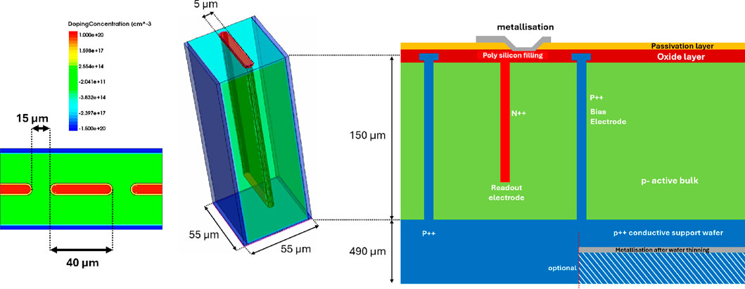
Figure 1. Structure and technological profile of the 3D trench sensor developed within the TimeSPOT project.
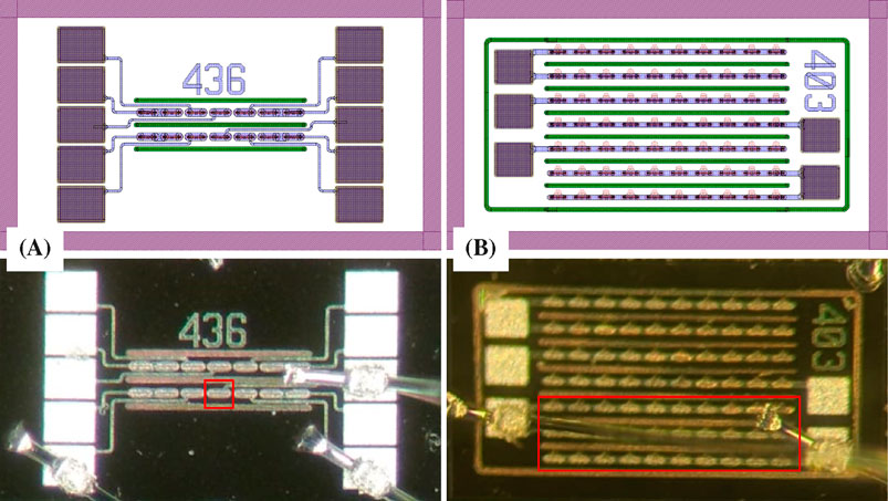
Figure 2. Layout and pictures of the 3D trench test structures tested at the CERN SPS: the single-pixel sensor (A) and the triple-strip sensor (B). For each structure the active area is outlined in red and is equal to 55 µm
2.2 Beam test setup
The irradiated 3D trench test structures were characterised with a 180 GeV/
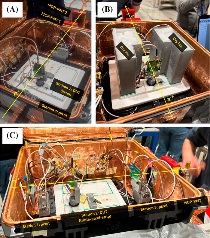
Figure 3. Pictures of test beam setups. (A) Charge collection efficiency and time resolution setup, with a single-pixel in Station 1 aligned to the DUT in Station 2; the two MCP-PMTs are also visible. (B) Front view of the light-tight box, where the containers fully filled with dry ice are visible. (C) Detection efficiency setup: the two single-pixels in Stations 1 and 3 are carefully aligned with respect to the triple-strip sensor (DUT), and the single MCP-PMT is visible outside the box. The yellow lines represent the beam direction.
Two station configurations were used: one for measuring the detection efficiency and the other for the charge collection efficiency and time resolution measurements. The setup for the detection efficiency (Figure 3C) included two non-irradiated pixels positioned in Stations 1 and 3 and one of the two MCP-PMTs. In this configuration, the trigger condition required a coincidence of signals from both Stations 1 and 3, while the DUT consisted of triple-strip irradiated at a given fluence. For time resolution and charge collection efficiency measurements, the pixel at Station 3 was removed (Figure 3A), and a second MCP-PMT was included in the acquisition to provide a more accurate time reference. In this configuration, the trigger condition was the coincidence of signals from Station 1 and one of the two MCP-PMTs, and the DUTs were single-pixel irradiated structures.
The signals from the silicon sensors and the MCP-PMTs were recorded by an 8 GHz analog bandwidth 20 GSa/s four-channels digital oscilloscope. The connection of the detectors to the oscilloscope was made through low-loss RF coaxial cables. The coincidence for the triggers required signals with a minimum amplitude in two detectors inside a time window of 20 ns. The trigger conditions used for both setup configurations avoid biases in the DUT, which was never included in the acquisition condition. An example of signals acquired for the efficiency measurements is shown in Figure 4.
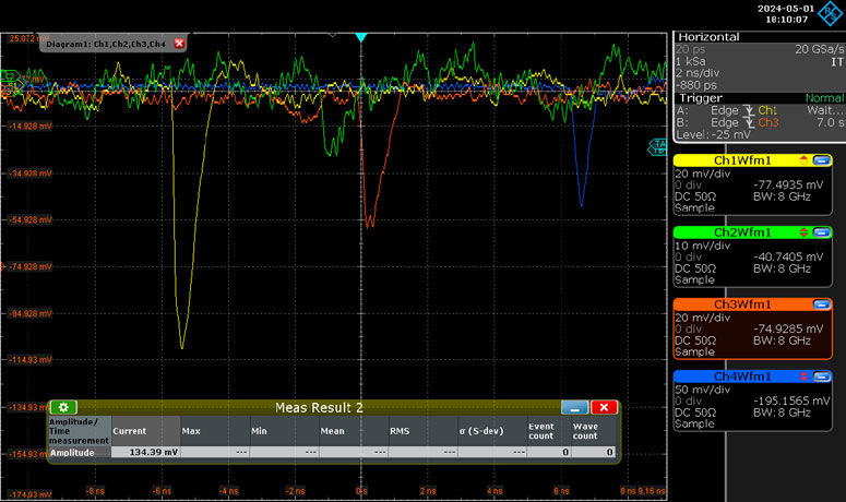
Figure 4. A typical event from the oscilloscope display in which a charged particle crosses the four detectors of the setup used for the efficiency measurements. The signals from the two triggering pixels are shown in yellow and orange, the signal of an irradiated triple-strip sensor is showed in green, while the signal from the MCP-PMT is reported in blue.
2.3 Analysis method
The analysis strategy is similar to that followed in previous test beam campaigns and is discussed in References [3, 9, 10]. The waveforms acquired by the oscilloscope were automatically saved as a time series of voltage samples, which were further processed using various software algorithms. To determine the signal amplitude, the baseline value was first calculated by fitting the initial samples of the waveform on an event-by-event basis with a constant function. The final amplitude was then obtained by subtracting this baseline value from the minimum value of the waveform. Different methods have been studied in past analyses for signal time measurement. In this analysis, two methods were used: the reference method and the spline method. The reference method applies the amplitude and rise-time compensation (ARC) algorithm [15], i.e., the signal waveform is delayed by approximately half of the signal rise-time, and a subtraction between the original and delayed waveform is performed, resulting in a new waveform with reduced correlated noise. The Time of Arrival (TOA) is then determined as the point where the subtracted waveform exceeds half of its maximum amplitude. The spline method refines the constant-fraction discrimination approach. To improve accuracy and reduce sensitivity to time digitization, the samples were first interpolated with a cubic spline, and the TOA was then determined as the point of the spline function corresponding to 20% of the peak amplitude. Although the reference method provides the best time resolution performance, the spline method is applied to obtain results with an algorithm potentially similar to a constant fraction discriminator that can be implemented in front-end electronics. After this pre-processing, the resulting dataset, containing all events with their corresponding amplitude and time measurements, is further statistically analysed as explained in the following sections.
2.3.1 Charge collection efficiency
Irradiation typically leads to a reduction in the Charge Collection Efficiency (CCE) of silicon sensors. To evaluate possible changes in the 3D trench pixels response after irradiation, the CCE analysis was performed on several test structures: non-irradiated, irradiated at
The calibration factor is calculated as the ratio of Most Probable Value (MPV) of the distributions of the charge in simulation and of the measured amplitude in data. The MPVs are obtained by fitting the distributions with a Landau probability density function convolved with a Gaussian function that models the smearing in data due to amplifier noise. A check on the calibration factor was done using samples corresponding to different tilt angles, where different charge deposits are expected. The results agree within uncertainties, and validate the assumption of a linear behaviour of the amplifier. The charge collection distribution are then obtained for all the tested structures by multiplying the signal amplitudes for the calibration factor. To account for the fact that irradiated sensors were tested at low temperatures, while the calibration factor is determined using data taken at room temperature, the amplifier gain variation as a function of temperature was studied using a climatic chamber at the INFN Cagliari laboratories. With respect to room temperature, a
2.3.2 Detection efficiency
Measurements of detector efficiency were performed using tracks hitting two 3D trench pixels along the beam line and a triple-strip as a DUT. The two single-pixels acted as the trigger whilst the time reference was provided by a single MCP-PMT. To minimise the overlap of the trench electrodes, the triple-strip was oriented such that its trenches were perpendicular to those of the trigger pixels.
The sensor efficiency
A track is considered detected by the DUT if its measured TOA is consistent with the expected time of flight. For this analysis the TOA of the DUT is reconstructed using the spline method. A histogram of the TOA difference between a triple-strip and the MCP-PMT for all triggered events is shown in Figure 5. The events detected by the DUT are located within the peak of the distribution, which is modeled by the sum of a Gaussian function and an exponential function convolved with a Gaussian. The non-detected tracks are reconstructed with a random TOA value, which follows a uniform distribution.
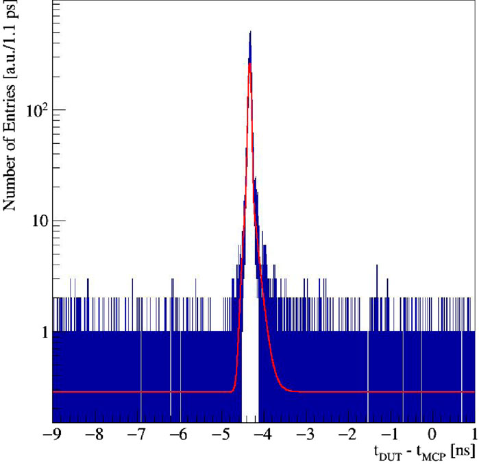
Figure 5. Distribution of the time difference between the triple-strip (DUT) and the MCP-PMT. The fit result is represented by the red line.
2.3.3 Time resolution
To accurately determine the DUT time resolution, the acquisition was triggered by the coincidence of signals detected in the single-pixel at Station 1 and in one of the two MCP-PMTs located downstream of the DUT. As explained in Section 2.2, the four devices were carefully aligned to maximize the rate of detected coincidences. The final measurement of time resolution is made with respect to the time reference given by the mean of the TOAs of the two MCP-PMTs
3 Results
3.1 Charge collection efficiency
To investigate the charge collection reduction and its mitigation by the increasing of the bias voltage, the charge collected by two 3D trench single-pixel structures irradiated at
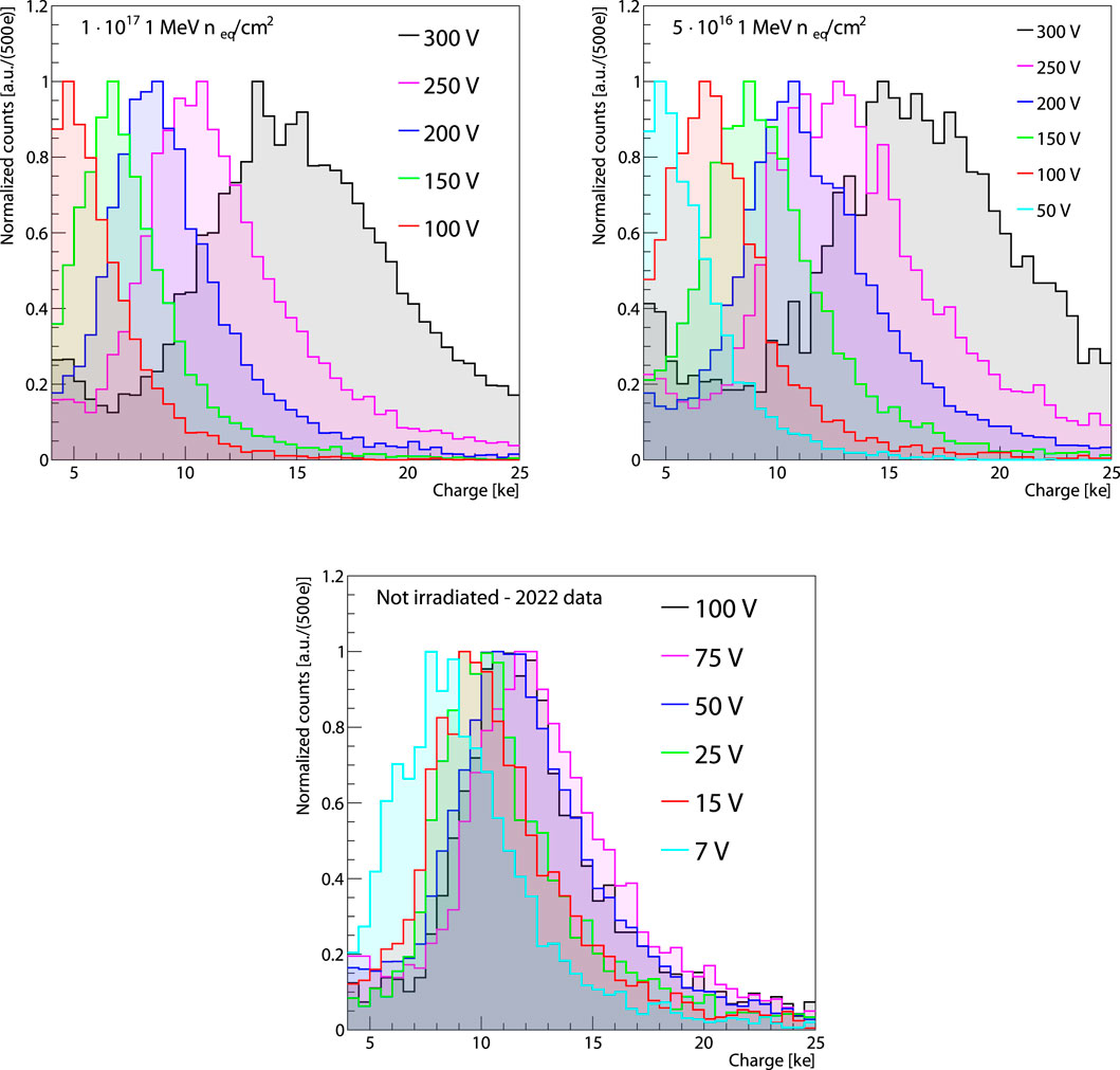
Figure 6. Normalized charge distributions, in electrons unit, as a function of bias voltage. (Top left) irradiated sensor at
Both irradiated pixels show a recovery in charge collection performance as the reverse bias voltage is increased, with the
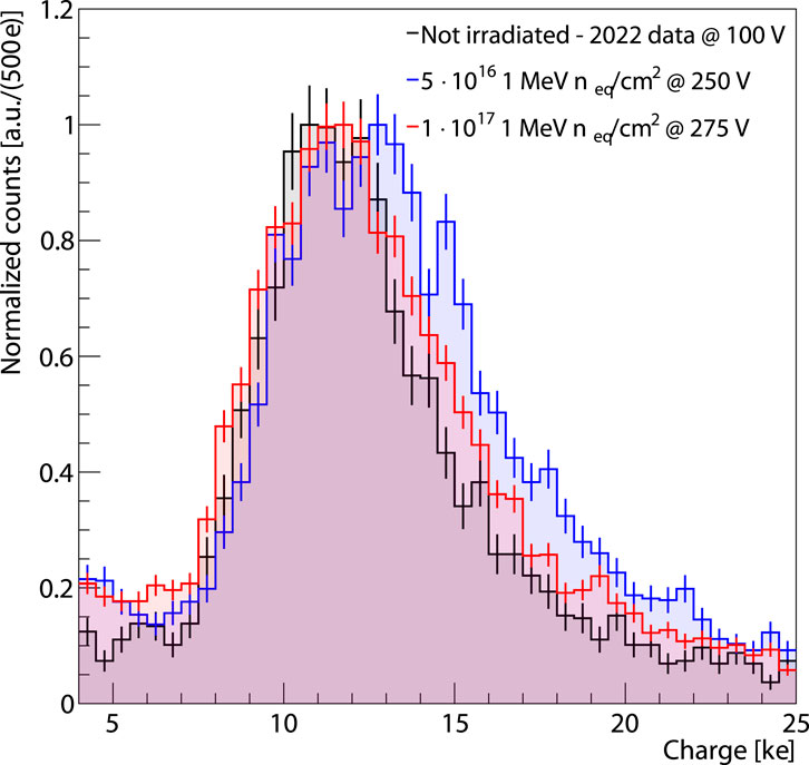
Figure 7. Normalized charge distributions, in electrons unit, of the
To make quantitative comparisons of charge collection efficiencies for the tested sensors, the MPVs of the charge distributions were plotted as a function of reverse bias voltage, as shown in Figure 8. Both irradiated sensors exhibit a similar trend, with the most irradiated one showing lower charge collection efficiency. In contrast, the non-irradiated sensor shows no significant dependence on reverse bias voltage beyond 50 V. The comparison of the MPVs indicates a full recovery of charge collection efficiency for both irradiated sensors, as qualitatively inferred from the distributions. Additionally, it reveals that sensors with higher irradiation levels require a greater reverse bias voltage to achieve this recovery.
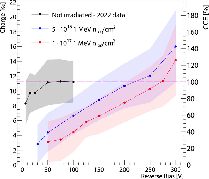
Figure 8. MPV of the charge distributions and Charge Collection Efficiency for the two irradiated and for the non-irradiated pixels as a function of the reverse bias voltage. The 100 V MPV data of the non-irradiated pixel have been used as a reference for the CCE evaluation. The colored areas represent the FWHM of the distributions.
When operating the sensors at higher bias voltages, close to 300 V, multiplication factors of approximately 1.4 for the
3.2 Detection efficiency
Detection efficiency was evaluated using the method detailed in Section 2.3.2. Since the trigger setup differed from that used in previous measurements [3, 10], the results with the new layout were first validated by measuring the efficiency of a non-irradiated sensor as a function of the incident beam angle. These results were found to be consistent with those reported in Reference [3], which are more comprehensive and will therefore be used for comparison with the new measurements in this article. The dependence of 3D trench detection efficiency on the tilt angle relative to normal incidence has been previously demonstrated [3, 10]. Since the trench electrodes are non-sensitive volumes, a recovery of detector efficiency is expected when tilting a 3D trench sensor with respect to the beam path. This effect has also been studied for the
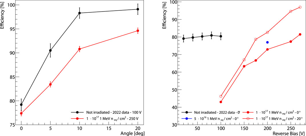
Figure 9. (Left) Detection efficiency as a function of tilt angle for a triple-strip sensor irradiated at
The impact of bias voltage on detection efficiency for the triple-strip irradiated at
Consistently, these measurements, along with those shown in the charge collection efficiency study, demonstrate that 3D trench sensors irradiated at very high fluences achieve similar detection performance to that of a non-irradiated sensor if operated at a sufficiently high reverse bias voltage.
3.3 Time resolution
This section reports the results of the time resolution studies on two 3D trench single-pixels irradiated at
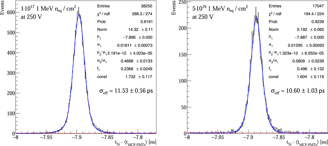
Figure 10. Distributions of the difference between the time of arrival of the 3D trench single-pixel (reference method) and the time reference,
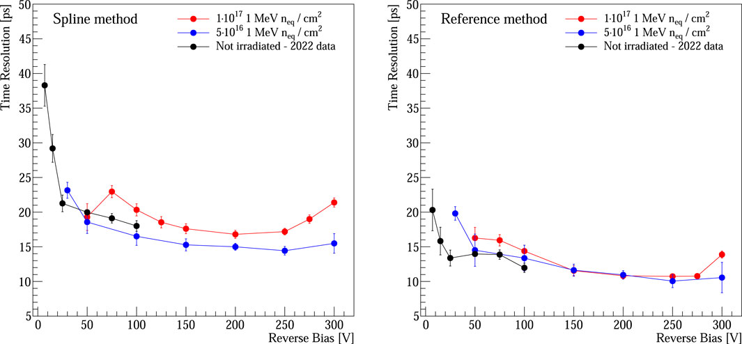
Figure 11. Time resolution of the single-pixels as a function of the reverse bias voltage for the different irradiation fluences obtained with the (right) reference method and (left) spline method. The contribution due to the resolution of the time reference is subtracted.
The sensors irradiated up to
The trend in Figure 11 shows that the time resolution does not improve significantly once the reverse bias voltage has surpassed 200 V. By further increasing the voltage to 300 V, a degradation in time resolution is observed, most likely due to impact ionization within the sensor, as previously discussed in Section 3.1. Moreover, by using the spline method, a slightly better timing performance it is observed for the sensors irradiated at
4 Discussion
The 3D trench silicon pixel sensors developed by the TimeSPOT collaboration have demonstrated remarkable performance in detecting high-energy charged particles, even after exposure to extreme radiation fluences. This study assessed the radiation tolerance of these sensors up to fluences of
Currently, 3D trench silicon detectors are among the fastest and most radiation-hard pixel sensors available for use in vertex detectors at high-energy physics colliders. The findings of this study further enhance the potential of these sensors for integration into the tracking systems of experiments at the Future Circular Hadron Collider (FCC-hh). This shifts the focus towards the development of low-power consumption readout ASICs for new vertex detectors, capable of meeting the enhanced radiation hardness standards set by 3D trench sensors.
Data availability statement
The raw data supporting the conclusions of this article will be made available by the authors, without undue reservation.
Author contributions
MA: Formal Analysis, Investigation, Methodology, Writing–original draft, Writing–review and editing. AB: Formal Analysis, Investigation, Methodology, Writing–original draft, Writing–review and editing. FB: Formal Analysis, Writing–review and editing. DB: Formal Analysis, Investigation, Methodology, Writing–original draft, Writing–review and editing. AC: Conceptualization, Investigation, Methodology, Writing–review and editing. GC: Conceptualization, Writing–review and editing. GD: Conceptualization, Writing–original draft, Writing–review and editing. LL: Investigation, Methodology, Writing–review and editing. ALi: Conceptualization, Investigation, Writing–review and editing. ALm: Conceptualization, Formal Analysis, Investigation, Methodology, Writing–original draft, Writing–review and editing. ALo: Conceptualization, Formal Analysis, Investigation, Writing–original draft, Writing–review and editing. MO: Formal Analysis, Investigation, Methodology, Writing–original draft, Writing–review and editing. SV: Formal Analysis, Investigation, Methodology, Writing–original draft, Writing–review and editing. MV: Conceptualization, Formal Analysis, Investigation, Methodology, Writing–original draft, Writing–review and editing.
Funding
The author(s) declare that financial support was received for the research, authorship, and/or publication of this article. This work was supported by the Fifth Scientific Commission (CSN5) of the Italian National Institute for Nuclear Physics (INFN), within the Project TimeSPOT and by the ATTRACT-EU initiative, INSTANT project. This project has received funding from the European Union’s Horizon 2020 Research and Innovation programme under GA no. 101004761. This project has received funding from the European Union’s Horizon Europe Research and Innovation program under Grant Agreement No 101057511 (EURO-LABS).
Acknowledgments
The authors wish to thank the staff of North Hall Area at CERN for their help in the beam-line setup and operations.
Conflict of interest
The authors declare that the research was conducted in the absence of any commercial or financial relationships that could be construed as a potential conflict of interest.
The author(s) declared that they were an editorial board member of Frontiers, at the time of submission. This had no impact on the peer review process and the final decision
Publisher’s note
All claims expressed in this article are solely those of the authors and do not necessarily represent those of their affiliated organizations, or those of the publisher, the editors and the reviewers. Any product that may be evaluated in this article, or claim that may be made by its manufacturer, is not guaranteed or endorsed by the publisher.
Footnotes
1https://www.newport.com/p/CONEX-SAG-LS32
References
1. Lampis A. Innovative silicon pixel sensors for a 4D VErtex LOcator detector for the LHCb high luminosity upgrade. Cagliari U: Ph.d. thesis (2023).
2. Kramberger G, Carulla M, Cavallaro E, Cindro V, Flores D, Galloway Z, et al. Radiation hardness of thin low gain avalanche detectors. Nucl Instr Methods Phys Res Section A: Acc Spectrometers, Detectors Associated Equipment (2018) 891:68–77. doi:10.1016/j.nima.2018.02.018
3. Borgato F, Cardini A, Cossu GM, Dalla Betta GF, Garau M, La Delfa L, et al. Characterisation of highly irradiated 3D trench silicon pixel sensors for 4d tracking with 10 ps timing accuracy. Front Phys (2024) 12. doi:10.3389/fphy.2024.1393019
4. Abada A, Abbrescia M, AbdusSalam SS, Abdyukhanov I, Abelleira Fernandez J, Abramov A, et al. Fcc-hh: the hadron collider: future circular collider conceptual design report volume 3. Eur Phys J Spec Top (2019) 228:755–1107. doi:10.1140/epjst/e2019-900087-0
5. Parker S, Kenney C, Segal J. 3D — a proposed new architecture for solid-state radiation detectors. Nucl Instr Methods Phys Res Section A: Acc Spectrometers, Detectors Associated Equipment (1997) 395:328–43. doi:10.1016/S0168-9002(97)00694-3
6. The LHCb Collaboration. Framework TDR for the LHCb upgrade II: opportunities in flavour physics, and beyond. In: Scientific committee paper (2021).
7. Forcolin G, Boscardin M, Ficorella F, Lai A, Loi A, Mendicino R, et al. 3D trenched-electrode pixel sensors: design, technology and initial results. Nucl Instr Methods Phys Res Section A: Acc Spectrometers, Detectors Associated Equipment (2020) 981:164437. doi:10.1016/j.nima.2020.164437
8. Loi A. Design and test of a timing optimized 3D silicon sensor for HL-LHC experiments (2020). Available from: https://hdl.handle.net/11584/284136 (Accessed 2020).
9. Anderlini L, Aresti M, Bizzeti A, Boscardin M, Cardini A, Dalla Betta GF, et al. Intrinsic time resolution of 3D-trench silicon pixels for charged particle detection. J Instrumentation (2020) 15:P09029. doi:10.1088/1748-0221/15/09/P09029
10. Borgato F, Brundu D, Cardini A, Cossu GM, Dalla Betta GF, Garau M, et al. Charged-particle timing with 10 ps accuracy using TimeSPOT 3D trench-type silicon pixels. Front Phys (2023) 11:1117575. doi:10.3389/fphy.2023.1117575
11. Brundu D, Cardini A, Contu A, Cossu GM, Dalla Betta GF, Garau M, et al. Accurate modelling of 3D-trench silicon sensor with enhanced timing performance and comparison with test beam measurements. J Instrumentation (2021) 16:P09028. doi:10.1088/1748-0221/16/09/p09028
12. Lea S, Žerovnik G, Trkov A. Computational analysis of irradiation facilities at the JSI TRIGA reactor. Appl Radiat Isot (2012) 70:483–8. doi:10.1016/j.apradiso.2011.11.042
13. Cossu GM, Lai A. Front-end electronics for timing with pico-second precision using 3D trench silicon sensors. J Instrumentation (2023) 18:P01039. doi:10.1088/1748-0221/18/01/P01039
14. Lampis A. Innovative silicon pixel sensors for a 4D VErtex LOcator detector for the LHCb high luminosity upgrade. Cagliari, Italy: University of Cagliari (2023). PhD Thesis.
15. Cho Z, Chase R. Comparative study of the timing techniques currently employed with Ge detectors. Nucl Instr Methods (1972) 98:335–47. doi:10.1016/0029-554X(72)90115-2
16. Loi A, Contu A, Lai A. Timing optimisation and analysis in the design of 3d silicon sensors: the tcode simulator. J Instrumentation (2021) 16:P02011. doi:10.1088/1748-0221/16/02/P02011
17. Cossu GM, Brundu D, Lai A. Intrinsic timing properties of ideal 3D-trench silicon sensor with fast front-end electronics. J Instrumentation (2023) 18:P07014. doi:10.1088/1748-0221/18/07/P07014
18. Koehler M, Bates R, Fleta C, Jakobs K, Lozano M, Parkes C, et al. Comparative measurements of highly irradiated n-in-p and p-in-n 3D silicon strip detectors. Nucl Instr Methods Phys Res Section A: Acc Spectrometers, Detectors Associated Equipment (2011) 659:272–81. doi:10.1016/j.nima.2011.08.041
19. Mendicino R, Boscardin M, Dalla Betta GF. Characterization of FBK small-pitch 3D diodes after neutron irradiation up to 3.5 × 10¹⁶ neq cm−2. J Instrumentation (2019) 14:C01005. doi:10.1088/1748-0221/14/01/C01005
Keywords: particle tracking detectors, solid-state detectors, timing detectors, 4D tracking, radiation hardness, high time resolution, high luminosity, FCC-hh
Citation: Addison M, Bellora A, Borgato F, Brundu D, Cardini A, Cossu GM, Dalla Betta GF, La Delfa L, Lai A, Lampis A, Loi A, Obertino MM, Vecchi S and Verdoglia M (2024) Characterisation of 3D trench silicon pixel sensors irradiated at 1
Received: 16 September 2024; Accepted: 21 October 2024;
Published: 19 November 2024.
Edited by:
Marco Mandurrino, National Institute of Nuclear Physics of Turin, ItalyReviewed by:
Simone Michele Mazza, University of California, Santa Cruz, United StatesMarkus Kuster, European X-Ray Free Electron Laser, Germany
Copyright © 2024 Addison, Bellora, Borgato, Brundu, Cardini, Cossu, Dalla Betta, La Delfa, Lai, Lampis, Loi, Obertino, Vecchi and Verdoglia. This is an open-access article distributed under the terms of the Creative Commons Attribution License (CC BY). The use, distribution or reproduction in other forums is permitted, provided the original author(s) and the copyright owner(s) are credited and that the original publication in this journal is cited, in accordance with accepted academic practice. No use, distribution or reproduction is permitted which does not comply with these terms.
*Correspondence: A. Lampis, YW5kcmVhLmxhbXBpc0BjYS5pbmZuLml0
 M. Addison
 A. Bellora2,3
 D. Brundu
 A. Cardini
 G. F. Dalla Betta
 A. Lai
 A. Lampis
 A. Loi
 S. Vecchi
 M. Verdoglia