 Hongdao Cheng1
 Jianhui Yu
 Yongchun Zhong
95% of researchers rate our articles as excellent or good
Learn more about the work of our research integrity team to safeguard the quality of each article we publish.
Find out more
ORIGINAL RESEARCH article
Front. Phys. , 29 July 2024
Sec. Optics and Photonics
Volume 12 - 2024 | https://doi.org/10.3389/fphy.2024.1446416
This article is part of the Research Topic Acquisition and Application of Multimodal Sensing Information - Volume II View all 9 articles
As a promising sensing material, Molybdenum disulfide (MoS2) nanosheets is being increasingly studied for Nitrogen dioxide (NO2) gas sensing. However, the MoS2 nanosheets is prone to the stacking effect that compromises the sensing performances. Here, the stacking effect is mitigated by engineering MoS2 nanosheets into a three dimensional (3D) network microstructure, which was fabricated by method of electrostatically self-assembling of MoS2/SiO2 microspheres. The fabricated sensor based on 3D MoS2 network observed a significantly improved response of 15% to 12.3 ppm NO2, which is a 75-fold increase compared to the control sensor with pure MoS2 nanosheets. In addition, the sensitivity of the sensor with 3D MoS2 network was 6.15 times larger than that of the control sensor with pure MoS2 nanosheets. The detection limit of our sensor was 0.297 ppm, lower than most of reported MoS2-based NO2 sensors. The enhanced sensitivity and dynamic response stem from the improved interaction between NO2 molecules and MoS2 network, thanks to its increased surface area per footprint of MoS2 nanosheets compared to pure 2D MoS2 film (single- or few-layer). This work presents a new approach to enhancing the performance of gas sensors based on 2D materials.
NO2 is a harmful gas pollutant that can pose a threat to environment and human health. The detection of NO2 is widely applied in industrial production [1], air quality monitoring [2], and environmental monitoring [3]. In recent years, NO2 detection with chemiresistive sensors has been widely investigated due to their low consumption and high accuracy [4]. Semiconductor metal oxides like TiO2 [5], SnO2 [6], ZnO [7], WO3 [8], Co3O4 [9], and NiO [10] are commonly used in gas sensing due to their excellent thermal stability, surface properties, tunable structure, and diverse surface morphology. To improve sensor sensitivity, metal oxide heterojunctions like Sn3O4/SnO2 [11], SnO2/In2O3 [12], and ZnO/SnO2 [13] are also utilized for NO2 gas detection. However, metal oxide gas sensors require high temperatures (100°C–300°C) for optimal performance. The need for high temperature necessitates additional heating elements, leading to higher operating and maintenance cost.
Recently, carbon materials [14, 15], transition-metal sulphides [16–18] have been used to detect NO2 for their ability to be used at room temperature. Because of the excellent electronic properties and high chemical stability, two dimensional materials such as graphene and its composites have attracted great attention for optoelectronic applications. Nevertheless, the zero bandgap and lower sensitivity limit their applications in gas sensing. MoS2 has been widely used for gas sensors due to its tunable band gap, large surface area ratio, and various active sites [19–22]. MoS2 grown by chemical vapor deposition method was used to detect NO2, achieved a low limit of detection (LOD) of 1 ppm [23, 24]. To increase the sensing characteristics, MoS2 nanoparticles such as flower-like nanospheres [11], nanoworms [25], nanoflakes [26] were used as the active materials. To overcome the disadvantage of fast electron-hole recombination caused by narrow bandgap of MoS2 (–1.65 eV) [27], various MoS2 compounds and doped MoS2 were also explored and achieved different success. For example, the LOD of the sensor based on MoS2/porous silicon nanowire heterojunctions reached 1 ppm [28]; By using MoS2/SnO2 compound as sensing material, Cui et al. fabricated a NO2 sensor whose LOD was 0.5 ppm [29]; In 2022, Bharathi et al. decreased the LOD to 0.311 ppm by using edge activated Ni-MoS2 nanosheets [30]. However, because MoS2 is a layered material and it usually suffers from sheet stacking, which seriously debilitates its sensing performance.
In this work, we demonstrated a NO2 sensor based on three dimensional MoS2 network microstructure, which can significantly enhance the sensitivity of MoS2-based NO2 sensor. The 3D MoS2 network microstructure was fabricated by using MoS2/SiO2 composite microspheres with a core-shell structure. The silicon dioxide (SiO2) microspheres serve as the support substrate, which were uniformly wrapped with MoS2 nanosheets on the spherical surface. This could prevent MoS2 nanosheets from the stacking effect and maintain the excellent electrical properties of MoS2 nanosheets. Furthermore, the formed 3D microstructure enhanced the interaction between NO2 molecules and MoS2 nanosheets, resulting in the improvement of the sensitivity and detection limitation of the sensor. This fabricated NO2 sensor exhibits high sensitivity and low LOD (0.297 ppm) at room temperature. Our fabricated gas sensor with 3D MoS2 network microstructure holds great potential for application potential in industrial production, monitoring under various conditions.
The preparation process of MoS2/SiO2 composite microspheres is shown in Figure 1 the MoS2/SiO2 composite microspheres are fabricated by electrostatic self-assembly method. Specifically, 7 mL emulsion of SiO2 microspheres (1.8 mg/mL, diameter is 1 μm, Da E Technology Co., Ltd.) and 30 μL Methacryloxyethyltrimethyl ammonium chloride (DMC) solution (concentration is 75%) were mixed and sonicated for 10 min. To make the SiO2 microspheres positively charged, the mixture was kept in a water bath at 75°C for 1.5 h. Then, 1.6 mL MoS2 nanosheet suspension (0.1 mg/mL, Beike 2D materials Co., Ltd.) is added to the positively charged SiO2 microspheres emulsion, mixed and stirred for 1.5 h to make sure the MoS2 nanosheets were completely and uniformly wrapped around the SiO2 microspheres.
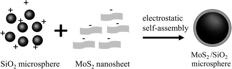
Figure 1. Preparation process of MoS2/SiO2 composite microspheres.
High resolution X-ray photoelectron spectroscopy (XPS, Thermo k alpha+, Thermo Fisher Scientific Inc.) was used to investigate the chemical nature of the MoS2 nanosheets, as depicted in Figure 2. The XPS spectra revealed signals of Mo 3d5/2 at 229.08 eV and Mo 3d3/2 at 232.18 eV, indicating the presence of Mo4+ [31]. This was further supported by the signals of S 2p3/2 and S 2p1/2 peaks at approximately 161.88 eV and 163.08 eV, corresponding to the S2- oxidation state of sulphur [32]. Additionally, peaks at 235.48 eV were attributed to Mo6+ in MoO3 due to surface oxidation and adsorption [33], while the presence of the S 2 s peak at 226.0 eV suggested oxidation of sulphur.
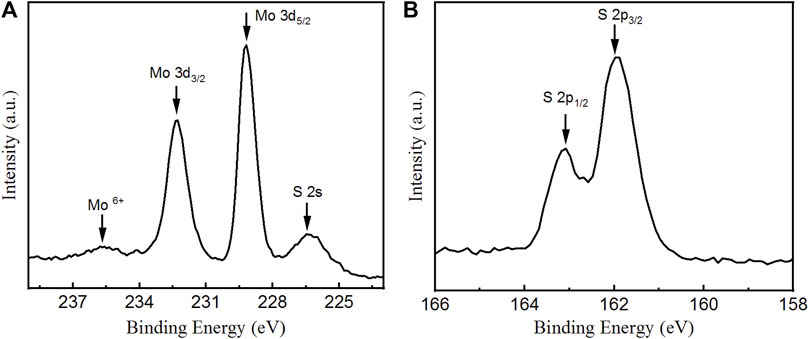
Figure 2. High resolution XPS spectra of MoS2 nanosheets (A) Mo 3d region and (B) S 2p region.
The SiO2 microspheres were coated around with MoS2 thin films as shown in the Figure 3A. The insert of Figure 3A shows the TEM image of typical MoS2 nanosheet, whose size is about 1 × 1 µm, so that the surface of the SiO2 microspheres should be encapsulated by about three nanosheets. As shown in the Figure 3B, the MoS2 nanosheets were uniformly wrapped around the SiO2 microspheres, forming a shell with thickness of 7.7 nm. The MoS2 coating consist of approximately ten layers. The MoS2 nanosheets did not exhibit significant stacking effects in the fabricated process of MoS2/SiO2 composite microspheres. Figures 3C–F is the energy dispersive spectrometers (EDSs) of the MoS2/SiO2 composite microspheres, while Figure 3G shows the corresponding TEM image of the EDSs. Figures 3C–F display the distributions of the Mo, S, Si, and O elements. The distribution patterns of Mo, S, Si, and O elements are similar and match the arrangement of the composite microspheres in TEM images (Figure 3G). It indicates that the MoS2 nanosheets were uniformly wrapped around the SiO2 microspheres. To confirm the existence of MoS2 coating on SiO2 microspheres, Raman spectroscopy of the composite microspheres is studied.
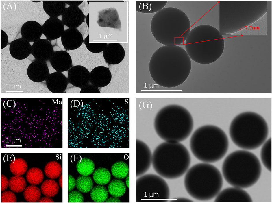
Figure 3. (A) (B) TEM images of MoS2/SiO2 composite microspheres; (C)-(G) TEM image and distribution of Mo, S, Si, and O elements of the MoS2/SiO2 composite microspheres.
Figure 4 shows the Raman spectra of MoS2/SiO2 microspheres and pure SiO2 microspheres, measured by Raman microspectroscopy (LabRAM HR Evolution, HORIBA Jobin Yvon, France, lens parameters: ×50 objective, NA = 0.5). In the Raman spectra of pure SiO2 microspheres (red solid curve), two broad peaks at 475.4 cm−1 and 795.5 cm−1 were observed. The peak at 475.4 cm−1 should be due to the W1 band (symmetrical Si-O-Si stretching modes) and the D1 defect band of SiO2. The peak at 795.5 cm−1 should be assigned as W2 band of SiO2 [34]. For the MoS2/SiO2 microspheres (dark solid curve), There are two main feature peaks at 383.5 cm−1 and 408.1 cm−1 in addition to the two broad peaks at 475.4 cm−1 and 795.5 cm−1. These two peaks at 383.5 cm−1 and 408.1 cm−1 are due to in-plane
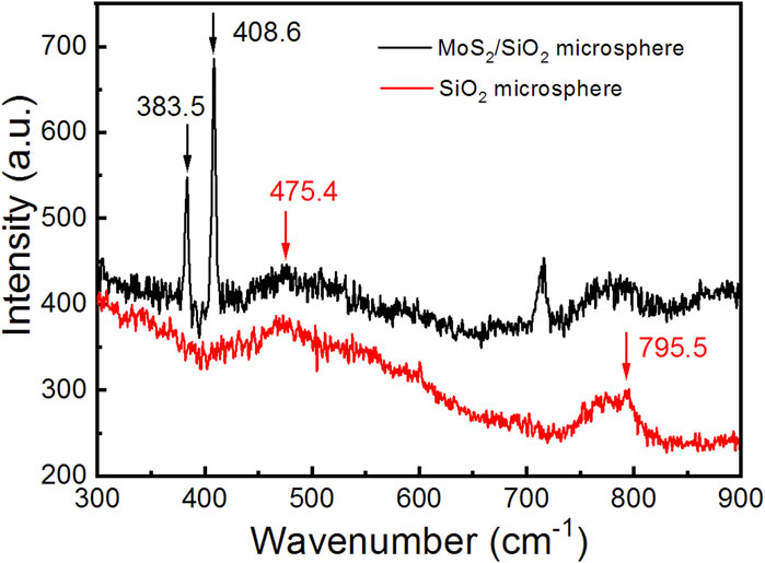
Figure 4. Raman spectra of MoS2/SiO2 composite microspheres and SiO2 microspheres.
Figure 5A is the fabrication process of the resistive gas sensor based on 3D MoS2 network. After 5 min of ultrasonic treatment, 4 μL of prepared MoS2/SiO2 composite microspheres suspension was dropped on the interdigitated electrodes (IDEs) by using a micro-syringe as shown in Figure 5A. After 6 hours of natural evaporation at room temperature, the composite microspheres were self-assembled and formed 3D MoS2 network structure on the IDEs. Figure 5B shows the Scanning Electron Microscope (SEM, Ultra-55, Carl Zeiss AG) image of the formed 3D MoS2 network structure. The MoS2/SiO2 composite microspheres were arranged into a 3D structure. As shown in the right insert in Figure 5B, the MoS2 nanosheets were uniformly wrapped around the SiO2 microsphere. The left insert of Figure 5B illustrates the cross section of the MoS2 3D network, which consists of more than 10 layers fabricated on the IDEs. The 3D structure appears uniform in Figure 5B.
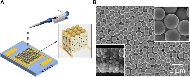
Figure 5. (A) The fabrication process of the MoS2/SiO2 composite microspheres wrapped on the interdigitated electrodes. (insert: schematic diagram of 3D MoS2 network structure) (B) SEM image of the 3D MoS2 network microstructure (left insert: the cross section of the 3D MoS2 network; right insert: magnified SEM image of microsphere).
As shown in the insert of Figure 5A, the SiO2 microspheres serve as the support substrate, which could avoid the stacking of MoS2 nanosheets and maintain the excellent electrical properties of MoS2 nanosheets. The MoS2 nanosheets (yellow region) wrapped around the SiO2 microspheres (gray region) were interconnected to form a 3D network resistance. This 3D network provides a larger surface area per footprint of MoS2 nanosheets compared to 2D single- or few-layer MoS2 film, increasing the contact area between gas molecules and MoS2 nanosheets to enhance the sensing response. However, the 3D network structure is not close-packed due to the uneven surface of the IDEs, resulting in a lower filling factor of microspheres and limiting the surface area per footprint of the MoS2 film.
Figure 6 is the setup of NO2 sensing experiment. Two individual flow controllers (MFC, Beijing Qixing Co., Ltd., China) were used to control the flow velocities of nitrogen and nitrogen dioxide. The concentrations of NO2 could be controlled by controlling the flow rates of nitrogen and nitrogen dioxide separately. The prepared sample was placed into a chamber with gold electrodes, which connected to the interdigital electrode of the sample. The impedance change of the sample was monitored by the impedance analyzer (UCE, UC8002, China) and the data was transmitted to the computer for display and saved in real time. The whole gas sensing experiment was carried out at room temperature.
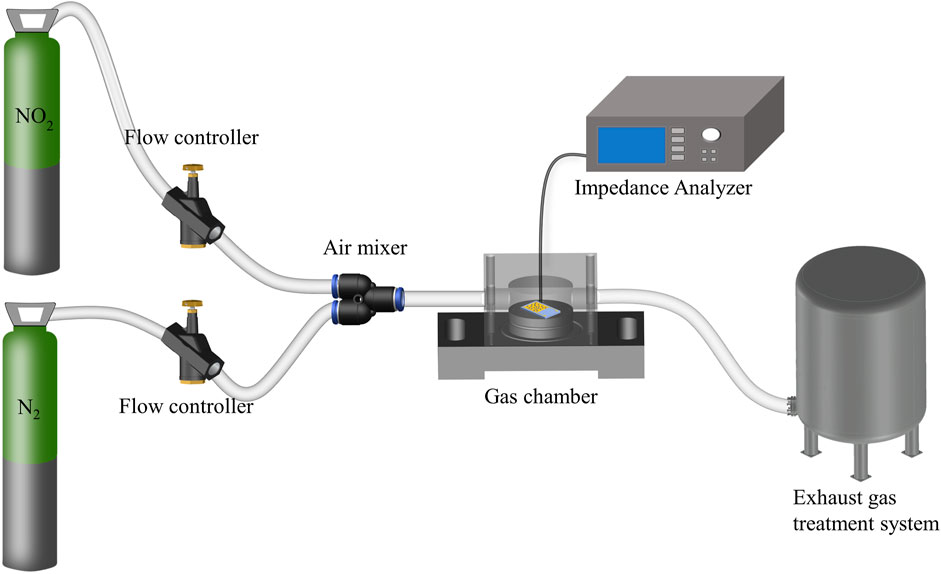
Figure 6. Experimental setup of NO2 sensing measurement.
The sensing response (S) of the sample was calculated by Eq. 1 [25]:
Where,
Figure 7 shows the NO2 sensing properties of MoS2 nanosheets with 3D network microstructure. The resistance of the MoS2 nanosheets with 3D network microstructure is 23.7 kΩ. The resistances of the sample decrease gradually with increasing NO2 gas concentration at room temperature (from 12.2 to 18.3 ppm), as shown in Figure 7. The variation amplitude of the sensing response (S) increases gradually with increasing NO2 gas concentration at room temperature (from 12.2 to 18.3 ppm). Figure 7B shows the sensing response of the sensor under different NO2 gas concentrations. The red line is the linear fitting of the sensing response. The sensitivity is 0.806%/ppm, and the linearity coefficient is 0.997.
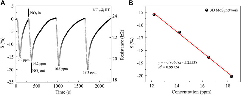
Figure 7. NO2 Gas sensing properties of MoS2 with 3D network microstructure: (A) the variation of actual sample’s response with different NO2 gas concentrations mixed with dry N2 at room temperature; (B) the response of the sensor under different NO2 gas concentrations and its linear fitting.
For comparison, the NO2 gas sensing characteristics of MoS2 nanosheets from the same batch were studied. Figure 8 shows the NO2 sensing characteristics of MoS2 nanosheets without 3D network microstructure. The resistance of the pure MoS2 nanosheets is 3703.8 kΩ, which is 156 times that of the sample with 3D network structure. As shown in the Figure 4, the 3D network microstructure has multiple connected MoS2 films, which greatly increases the conductive paths and reduces the resistance of the MoS2 3D network microstructure sample. As expected, the pure MoS2 sensor exhibit a similar trend for the response to NO2 gas concentration at room temperature (from 12.3 to 18.4 ppm). However, the obtained sensitivity of 0.131%/ppm is remarkably lower as shown in Figure 8B. In another word, by employing the 3D MoS2 network, the sensitivity of the sensor is improved by 6.15 times, compared to the control sensor using pure MoS2 nanosheets. When the concentration of NO2 was 12.2 ppm, the response of MoS2 nanosheets with 3D network microstructure was up to 15%. It is 75 times larger than that of MoS2 nanosheets sample (0.2%). The improvement in sensing performance is due to the 3D network microstructure, which greatly increases the contact area between MoS2 nanosheets and gas molecules.
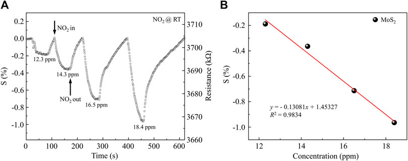
Figure 8. NO2 gas sensing properties of MoS2 nanosheets: (A) the variation of actual sample’s response with different NO2 gas concentrations mixed with dry N2 at room temperature; (B) the response of the sensor under different NO2 gas concentrations and its linear fitting.
The limit of detection can be calculated using the following Eq. 2 [30],
where the Std.deviation is the standard deviation of the base line, 3 denotes that the value of the response is three times higher than the noise level of the sensor device. The calculated LOD of the sensor base on 3D MoS2 network was 297 ppb, whereas the value for the sensor based on pure MoS2 nanosheets was much larger, 727 ppb. The LOD of the sensor with 3D MoS2 is 2.45 times lower than that of the control sensor with pure MoS2.
Figure 9 shows the characterization of repeatability, stability and dynamic response of the sensor based on 3D MoS2 network. As shown in Figure 9A, the NO2 concentration was continuously changed between 0 ppm and 12.3 ppm at room temperature, the sensor keeps their original response without apparent degradation, which indicated that the sensor has good repeatability and stability. The response and recovery times of the sensor (detecting 12.3 ppm at room temperature) is investigated as shown in Figure 9B. The response (Tres) and recovery time (Trec) of the gas sensor based on 3D MoS2 network were 57 s and 204 s, respectively. This sensor exhibited a quicker dynamic response compared to MoS2/SnO2 sensor when exposed to a NO2 concentration of 10 ppm level [29].
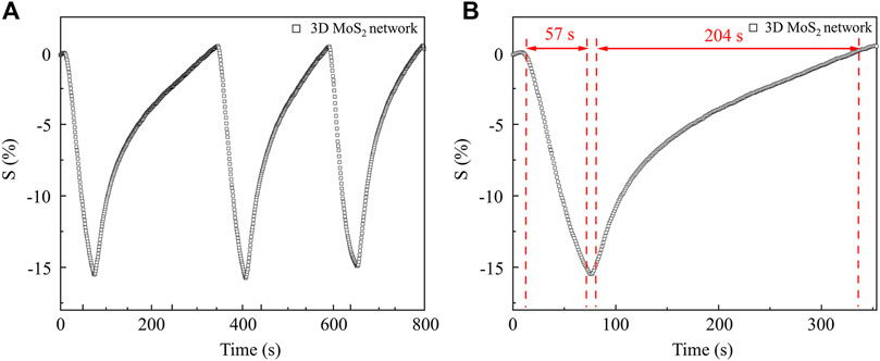
Figure 9. (A) the characterization of repeatability, stability of the sensor based on 3D MoS2 network; (B) dynamic response of the sensor based on 3D MoS2 network.
The sensing response is influenced by the concentration of charge carriers in the sensing materials. It can be proven through first principles that the adsorption of NO2 gas on MoS2 causes the Fermi level to shift downwards to the valence band, which leads to hole doping in MoS2 [35]. The Eq. 3 shows the proposed chemical interaction mechanism:
In our experiment, when NO2 is adsorbed, the resistance of both MoS2-based sensors decreases, demonstrating a p-type sensing behavior. Both n-type and p-type MoS2 sensors have been reported [24–30] with different reason such as intrinsic defects, vacancies, and extrinsic defects. In the XPS spectra (Figure 2A), the peak at 235.48 eV confirms the presence of Mo6+ in MoS2 nanosheets, indicating that MoS2 was partially oxidized. Previous works has revealed that partial oxidation can introduce p-type doping [36, 37] and the MoOx layer between metal contacts and MoS2 can lead to p-type MoS2 transistor behavior [38]. It should be the reason for the p-type sensing behavior of our samples.
The significantly improved performance of 3D MoS2 network based sensor can be explained as follow. The SiO2 microspheres serve as the support substrate, which could efficiently prevent the MoS2 nanosheets from sticking together, allowing for the maximum utilization of the extensive surface area of MoS2 nanosheets. Assuming the MoS2/SiO2 composit microspheres assemble into a hexagonal close-packed (HCP) structure, the surface area of the 3D MoS2 networks is increased by a factor of
where Ssphere is the superficial area of the MoS2/SiO2 sphere with a radia of r, SHex is the area of a regular hexagon footprintprint with a width equal to 2r, 3 denotes that three MoS2/SiO2 spheres can be accommodated within each regular hexagon footprint, and the N is the number of layers in the 3D HCP structure. This 3D MoS2 network provides a larger surface area per footprint compared to 2D MoS2 films, increasing the contact area between gas molecules and MoS2 nanosheets to enhance the sensing response and reduce LOD.
Table 1 compares the performance of different NO2 gas sensors utilizing MoS2 at room temperature. As shown in Table 1, the sensor based on 3D MoS2 network exhibits high responsivity in measuring a concentration of 12.3 ppm. In comparison to hollow MoS2 spheres with a thickness of 700 nm [39], the MoS2 film supported by SiO2 can maintain a much thinner thickness of 7.7 nm. This helps prevent the stacking of molybdenum disulfide nanosheets and preserves its excellent electrical properties. Additionally, the self-assembly process forms up to 10 layers of a 3D connected network microstructure. As a result, our sensor can operate at room temperature and has a greater sensing response. It is worth noting that sensors based on MoS2 Flakes or MoS2/SnO2 show higher responsivities [26, 29], but the response time is notably longer that could be a critical shortcoming for practical applications. Thanks to the special structural features of 3D MoS2 network, our sensor demonstrates a visibly faster response time and moderate recovery time, while maintaining a satisfactory responsivity. Additionally, the limit of detection (0.297 ppm) is lower than the majority of NO2 sensors utilizing MoS2.
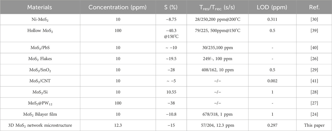
Table 1. Performance of different type of NO2 gas sensor based on MoS2 operating at room temperature.
We demonstrated a NO2 gas sensor operating at room temperature with excellent repeatability, low detection limit, and fast dynamic response. The sensor utilizes 3D MoS2 network microstructure, which was made by the method of electrostatically self-assembling of MoS2/SiO2 microspheres upon drop casting. Compared to the pristine 2D MoS2 nanosheets, the engineered 3D MoS2 network possess larger surface area per footprint and hence more active sites that facilitate the interaction between NO2 molecules and MoS2 nanosheets. This leads to the significantly improved sensitivity and dynamic response in the NO2 sensor with 3D MoS2 network. At a NO2 concentration of 12.2 ppm, the MoS2 nanosheets featuring a 3D network microstructure exhibited a response rate of 15%. This was a remarkable 75-fold increase compared to the response of the pristine MoS2 nanosheets sample. The detection limit of this sensor is 0.297 ppm, which is lower than the majority of NO2 sensors utilizing MoS2, as shown in Table 1. Additionally, this sensor exhibits fast response and recovery times of 57 s and 204 s, respectively. This high-performance NO2 gas sensor has potential applications in industrial production and indoor air quality monitoring. This work presents a new approach to enhancing the performance of gas sensors based on 2D materials.
The original contributions presented in the study are included in the article/Supplementary Material, further inquiries can be directed to the corresponding author.
HC: Data curation, Formal Analysis, Investigation, Writing–original draft. SH: Investigation, Data curation, Writing–original draft. ZX: Investigation, Methodology, Writing–review and editing, Supervision. LY: Data curation, Investigation, Writing–original draft. JY: Supervision, Writing–review and editing, Funding acquisition, Conceptualization. YZ: Supervision, Writing–review and editing, Funding acquisition, Conceptualization, Data curation.
The author(s) declare that financial support was received for the research, authorship, and/or publication of this article. National Natural Science Foundation of China (12174156); Natural Science Foundation of Guangdong Province (2017A030313359 and 2021A1575012632); Science and Technology Project of Guangzhou (201803020023).
The authors declare that the research was conducted in the absence of any commercial or financial relationships that could be construed as a potential conflict of interest.
All claims expressed in this article are solely those of the authors and do not necessarily represent those of their affiliated organizations, or those of the publisher, the editors and the reviewers. Any product that may be evaluated in this article, or claim that may be made by its manufacturer, is not guaranteed or endorsed by the publisher.
1. Tunlathorntham S, Thepanondh S. Prediction of ambient nitrogen dioxide concentrations in the vicinity of industrial complex area, Thailand. Air Soil Water Res (2017) 10:117862211770090. doi:10.1177/1178622117700906
2. Seow WJ, Downward GS, Wei H, Rothman N, Reiss B, Xu J, et al. Indoor concentrations of nitrogen dioxide and sulfur dioxide from burning solid fuels for cooking and heating in Yunnan Province, China. Indoor Air (2016) 26(5):776–83. doi:10.1111/ina.12251
3. Zhao X, Zhi M, Hang D, Ren Q, Zhang P, Chen C, et al. Ultrasensitive NO2 gas sensor based on MoS2 modified urchin-like Bi2S3 heterojunction. Physica E: Low-dimensional Syst Nanostructures (2023) 147:115575. doi:10.1016/j.physe.2022.115575
4. Huang D, Yang Z, Li X, Zhang L, Hu J, Su Y, et al. Three-dimensional conductive networks based on stacked SiO2@graphene frameworks for enhanced gas sensing. Nanoscale (2017) 9(1):109–18. doi:10.1039/C6NR06465E
5. Kumaresan M, Venkatachalam M, Saroja M, Gowthaman P, Gobinath J. Metal organic frameworks-derived sensing material of TiO2 thin film sensors for detection of NO2 gas. J Mater Sci Mater Electronics (2023) 34(5):400. doi:10.1007/s10854-023-09830-9
6. Lu Z, Pei X, Wang T, Gu K, Yu N, Wang M, et al. Oxidation-enabled SnS conversion to two-dimensional porous SnO2 flakes towards NO2 gas sensing. Dalton Trans (2024) 53(7):3027–38. doi:10.1039/D3DT03597B
7. Godse PR, Kadam SA, Nimbalkar TM, Jadhav YM, Jadhao YB, Ma Y-R, et al. Ultra-responsive and highly sensitive 1D ZnO nanotubes for detecting perilous low levels of NO2 gas. Mater Adv (2024) 5(7):2826–40. doi:10.1039/D3MA00962A
8. Hingangavkar GM, Navale YH, Nimbalkar TM, Mulik RN, Patil VB. Hydrothermally engineered WO3 nanoflowers: a selective detection towards toxic NO2 gas. Sensors Actuators B: Chem (2022) 371:132584. doi:10.1016/j.snb.2022.132584
9. Yuan Z, Zhao J, Meng F, Qin W, Chen Y, Yang M, et al. Sandwich-like composites of double-layer Co3O4 and reduced graphene oxide and their sensing properties to volatile organic compounds. J Alloys Compounds (2019) 793:24–30. doi:10.1016/j.jallcom.2019.03.386
10. Gomaa MM, Sayed MH, Patil VL, Boshta M, Patil PS. Gas sensing performance of sprayed NiO thin films toward NO2 gas. J Alloys Compounds (2021) 885:160908. doi:10.1016/j.jallcom.2021.160908
11. Zeng W, Liu Y, Mei J, Tang C, Luo K, Li S, et al. Hierarchical SnO2–Sn3O4 heterostructural gas sensor with high sensitivity and selectivity to NO2. Sensors Actuators B: Chem (2019) 301:127010. doi:10.1016/j.snb.2019.127010
12. Park S, Jung YW, Ko GM, Jeong DY, Lee C. Enhanced NO2 gas sensing performance of the In2O3-decorated SnO2 nanowire sensor. Appl Phys A (2021) 127(12):898. doi:10.1007/s00339-021-05063-x
13. Bai M, Chen M, Li X, Wang Q. One-step CVD growth of ZnO nanorod/SnO2 film heterojunction for NO2 gas sensor. Sensors Actuators B: Chem (2022) 373:132738. doi:10.1016/j.snb.2022.132738
14. Chung MG, Kim DH, Lee HM, Kim T, Choi JH, Dk S, et al. Highly sensitive NO2 gas sensor based on ozone treated graphene. Sensors Actuators B: Chem (2012) 166-167:172–6. doi:10.1016/j.snb.2012.02.036
15. Lee SW, Lee W, Hong Y, Lee G, Yoon DS. Recent advances in carbon material-based NO2 gas sensors. Sensors Actuators B: Chem (2018) 255:1788–804. doi:10.1016/j.snb.2017.08.203
16. Luo J, Li C, Yang Q, Yan L, Zhang B, Tao R, et al. Facile fabrication of MoS2 nanoflowers/SnO2 colloidal quantum dots nanocomposite for enhanced NO2 sensing at room temperature. IEEE Sensors J (2022) 22(7):6295–302. doi:10.1109/JSEN.2022.3151068
17. Zhao S, Shen Y, Zhou P, Zhang J, Zhang W, Chen X, et al. Highly selective NO2 sensor based on p-type nanocrystalline NiO thin films prepared by sol–gel dip coating. Ceramics Int (2018) 44(1):753–9. doi:10.1016/j.ceramint.2017.09.243
18. Zhang Y, Zeng W, Li Y. Hydrothermal synthesis and controlled growth of hierarchical 3D flower-like MoS2 nanospheres assisted with CTAB and their NO2 gas sensing properties. Appl Surf Sci (2018) 455:276–82. doi:10.1016/j.apsusc.2018.05.224
19. Li W, Zhang Y, Long X, Cao J, Xin X, Guan X, et al. Gas sensors based on mechanically exfoliated MoS2 nanosheets for room-temperature NO2 detection. Sensors (2019) 19(9):2123. doi:10.3390/s19092123
20. Park SY, Kim YH, Lee SY, Sohn W, Lee JE, Kim DH, et al. Highly selective and sensitive chemoresistive humidity sensors based on rGO/MoS2 van der Waals composites. J Mater Chem A (2018) 6(12):5016–24. doi:10.1039/C7TA11375G
21. Song J, Lou H. Improvement of gas-adsorption performances of Ag-functionalized monolayer MoS2 surfaces: a first-principles study. J Appl Phys (2018) 123(17):175303. doi:10.1063/1.5022829
22. Su S, Lv W, Zhang T, Tan Q, Zhang W, Xiong J. A MoS2 nanoflakes-based LC wireless passive humidity sensor. Sensors (2018) 18(12):4466. doi:10.3390/s18124466
23. Cho B, Hahm MG, Choi M, Yoon J, Kim AR, Lee Y-J, et al. Charge-transfer-based gas sensing using atomic-layer MoS2. Scientific Rep (2015) 5(1):8052. doi:10.1038/srep08052
24. Xu T, Pei Y, Liu Y, Wu D, Shi Z, Xu J, et al. High-response NO2 resistive gas sensor based on bilayer MoS2 grown by a new two-step chemical vapor deposition method. J Alloys Compounds (2017) 725:253–9. doi:10.1016/j.jallcom.2017.06.105
25. Neetika KA, Chandra R, Malik VK. MoS2 nanoworm thin films for NO2 gas sensing application. Thin Solid Films (2021) 725:138625. doi:10.1016/j.tsf.2021.138625
26. Kumar R, Goel N, Kumar M. UV-activated MoS2 based fast and reversible NO2 sensor at room temperature. ACS Sensors (2017) 2(11):1744–52. doi:10.1021/acssensors.7b00731
27. Wang P, Wang T, Li F, Li D, Yang Y, Yu H, et al. Enhanced sensing response of the first polyoxometalate electron acceptor modified MoS2 for NO2 gas detection at room temperature. Sensors Actuators B: Chem (2023) 382:133495. doi:10.1016/j.snb.2023.133495
28. Zhao S, Li Z, Wang G, Liao J, Lv S, Zhu Z. Highly enhanced response of MoS2/porous silicon nanowire heterojunctions to NO2 at room temperature. RSC Adv (2018) 8(20):11070–7. doi:10.1039/C7RA13484C
29. Cui S, Wen Z, Huang X, Chang J, Chen J. Stabilizing MoS2 nanosheets through SnO2 nanocrystal decoration for high-performance gas sensing in air. Small (2015) 11(19):2305–13. doi:10.1002/smll.201402923
30. Bharathi P, Harish S, Mathankumar G, Krishna Mohan M, Archana J, Kamalakannan S, et al. Solution processed edge activated Ni-MoS2 nanosheets for highly sensitive room temperature NO2 gas sensor applications. Appl Surf Sci (2022) 600:154086. doi:10.1016/j.apsusc.2022.154086
31. Sarma S, Ray SC. Trigonal (1T) and hexagonal (2H) mixed phases MoS2 thin films. Appl Surf Sci (2019) 474:227–31. doi:10.1016/j.apsusc.2018.02.218
32. Jha SK, Kumari R, Choudhary S, Guha P, Satyam P, Yadav BS, et al. Facile synthesis of semiconducting ultrathin layer of molybdenum disulfide. j nanosci nanotechnol (2018) 18(1):614–22. doi:10.1166/jnn.2018.13931
33. Dam S, Thakur A, Hussain S. Valence band studies of MoS2 thin films synthesised by electrodeposition method. Mater Today Proc (2021) 46:6127–31. doi:10.1016/j.matpr.2020.03.722
34. Hemley RJ, Mao HK, Bell PM, Mysen BO. Raman spectroscopy of SiO2 glass at high pressure. Phys Rev Lett (1986) 57(6):747–50. doi:10.1103/PhysRevLett.57.747
35. Salih E, Ayesh AI. First principle study of transition metals codoped MoS2 as a gas sensor for the detection of NO and NO2 gases. Physica E: Low-dimensional Syst Nanostructures (2021) 131:114736. doi:10.1016/j.physe.2021.114736
36. Sim DM, Kim M, Yim S, Choi M-J, Choi J, Yoo S, et al. Controlled doping of vacancy-containing few-layer MoS2 via highly stable thiol-based molecular chemisorption. ACS Nano (2015) 9(12):12115–23. doi:10.1021/acsnano.5b05173
37. Nan H, Wang Z, Wang W, Liang Z, Lu Y, Chen Q, et al. Strong photoluminescence enhancement of MoS2 through defect engineering and oxygen bonding. ACS Nano (2014) 8(6):5738–45. doi:10.1021/nn500532f
38. Chuang S, Battaglia C, Azcatl A, McDonnell S, Kang JS, Yin X, et al. MoS2 P-type transistors and diodes enabled by high work function MoOx contacts. Nano Lett (2014) 14(3):1337–42. doi:10.1021/nl4043505
39. Li Y, Song Z, Li Y, Chen S, Li S, Li Y, et al. Hierarchical hollow MoS2 microspheres as materials for conductometric NO2 gas sensors. Sensors Actuators B: Chem (2019) 282:259–67. doi:10.1016/j.snb.2018.11.069
40. Xin X, Zhang Y, Guan X, Cao J, Li W, Long X, et al. Enhanced performances of PbS quantum-dots-modified MoS2 composite for NO2 detection at room temperature. ACS Appl Mater Inter (2019) 11(9):9438–47. doi:10.1021/acsami.8b20984
Keywords: molybdenum disulfide, gas sensing, three dimensional network microstructure, nitrogen dioxide, two dimensional materials
Citation: Cheng H, Huang S, Xing Z, Yang L, Yu J and Zhong Y (2024) Enhanced sensing response of the three dimensional MoS2 microstructure for NO2 gas detection at room temperature. Front. Phys. 12:1446416. doi: 10.3389/fphy.2024.1446416
Received: 09 June 2024; Accepted: 12 July 2024;
Published: 29 July 2024.
Edited by:
Xukun Yin, Xidian University, ChinaReviewed by:
Qixin He, Beijing Jiaotong University, ChinaCopyright © 2024 Cheng, Huang, Xing, Yang, Yu and Zhong. This is an open-access article distributed under the terms of the Creative Commons Attribution License (CC BY). The use, distribution or reproduction in other forums is permitted, provided the original author(s) and the copyright owner(s) are credited and that the original publication in this journal is cited, in accordance with accepted academic practice. No use, distribution or reproduction is permitted which does not comply with these terms.
*Correspondence: Yongchun Zhong, eWNoemhvbmdAMTYzLmNvbQ==
Disclaimer: All claims expressed in this article are solely those of the authors and do not necessarily represent those of their affiliated organizations, or those of the publisher, the editors and the reviewers. Any product that may be evaluated in this article or claim that may be made by its manufacturer is not guaranteed or endorsed by the publisher.
Research integrity at Frontiers
Learn more about the work of our research integrity team to safeguard the quality of each article we publish.