 Sergey V. Uchaikin1*
 Jinmyeong Kim1,2Caǧlar Kutlu1,2Boris I. Ivanov1Jinsu Kim1Arjan F. van Loo3,4Yasunobu Nakamura3,4
 Saebyeok Ahn1Seonjeong Oh1Minsu Ko1,2
 Yannis K. Semertzidis1,2
- 1Center for Axion and Precision Physics Research, Institute for Basic Science (IBS), Daejeon, Republic of Korea
- 2Department of Physics, Korea Advanced Institute of Science and Technology (KAIST), Daejeon, Republic of Korea
- 3RIKEN Center for Quantum Computing (RQC), Wako, Japan
- 4Department of Applied Physics, Graduate School of Engineering, The University of Tokyo, Bunkyo-ku, Japan
This paper provides a comprehensive overview of the development of flux-driven Josephson Parametric Amplifiers (JPAs) as Quantum Noise Limited Amplifier for axion search experiments conducted at the Center for Axion and Precision Physics Research (CAPP) of the Institute for Basic Science. It focuses on the characterization, and optimization of JPAs, which are crucial for achieving the highest sensitivity in axion particle detection. We discuss various characterization techniques, methods for improving bandwidth, and the attainment of ultra-low noise temperatures. JPAs have emerged as indispensable tools in CAPP’s axion search endeavors, playing a significant role in advancing our understanding of fundamental physics and unraveling the mysteries of the Universe.
1 Introduction
CAPP was established in October 2013, entering the realm of axion physics following the notable contributions of experiments like the Axion Dark Matter Experiment (ADMX), Haloscope At Yale Sensitive To Axion Cold dark matter (HAYSTAC), etc. [1–4]. These experiments paved the way for axion research, and CAPP aimed to build on these achievements. It focused on establishing itself as a significant player in the field by pushing the boundaries in all relevant parameters and expanding the detection sensitivity.
It is extremely difficult to observe axions because of their weak interactions with Standard Model (SM) fields. In the presence of a magnetic field, an axion with a mass of
where
Here,
2 Haloscope
The axion haloscope employs a cavity with a high-quality factor, positioned within a strong magnetic field for the detection of signals arising when the axion frequency aligns with the cavity’s resonance. For the output signal power in haloscope experiments a larger magnetic field and cavity volume result in a greater conversion of axions into microwave photons (Eq. 3) [11]:
where
where
In haloscope experiments, the typical cavity shape is cylindrical, fitting efficiently into the design of a regular solenoid superconducting magnet, making optimal use of the magnet’s bore volume. The cavity commonly utilizes the
To access the cavity signal, a movable antenna is employed to optimize the coupling
The signal frequency is linked to the axion’s mass
Consequently, the scanning frequency rate is inversely proportional to the square of the total system noise. Hence, one of our primary goals is to minimize it, thereby augmenting of our scanning speed. System noise emanates from multiple sources within our setup, encompassing noise generated by the cavity, other passive components and the amplifiers. To achieve the lowest noise levels, it is imperative to cool down all readout components to temperatures lower than,
The most advanced amplifiers are capable of approaching noise levels close to the quantum limit. This article is dedicated to the adaptation and application of such amplifiers. In the following sections, we will elaborate on our measurement techniques for the JPAs, present their key parameters, and showcase both single JPA and multiple JPA readouts, including their respective noise characteristics.
3 Flux-driven JPA
In the earlier stages of CAPP axion search experiments, such as CAPP-9 T and CAPP-PACE [17, 18], we utilized state-of-the-art semiconductor amplifiers. The InP high-electron-mobility transistor (HEMT) is renowned for its ability to provide the lowest noise temperature in cryogenic low noise amplifier (LNA) applications. We employed the amplifiers LNF-LNC06_2A, manufactured by Low Noise Factory, which is specifically designed for cryogenic use [19]. These devices exhibit exceptionally low noise temperatures, reaching about 1.2 K when operated at temperatures below 10 K for frequencies around 1 GHz [20]. These experiments demonstrated CAPP’s capability to create a high-quality radio-frequency (RF) tunable cavity, maintain low temperatures, and operate a strong superconducting magnet in persistent mode [17, 18]. It also provided invaluable experience in data collection and processing. However, readouts chain based on cryogenic HEMT amplifiers have noise levels several tens of times higher than the quantum noise limit. For this case it would take several decades to scan the range between 1 and 2 GHz with DFSZ sensitivity.
3.1 JPA design
Despite significant advancements in the simulation and development of wideband Josephson amplifiers, such as traveling wave JPAs and impedance-transformed parametric amplifiers (see, for instance [21–32]), we have not identified one that operates within our required frequency range and maintains consistent 10 kHz frequency increments for gain and noise characterization across the entire range from 1 to 2 GHz. To achieve near-quantum-noise-limited amplification, we use a flux-driven JPA designed and fabricated for these experiments in RIKEN and the University of Tokyo [33]. This JPA design consists of a
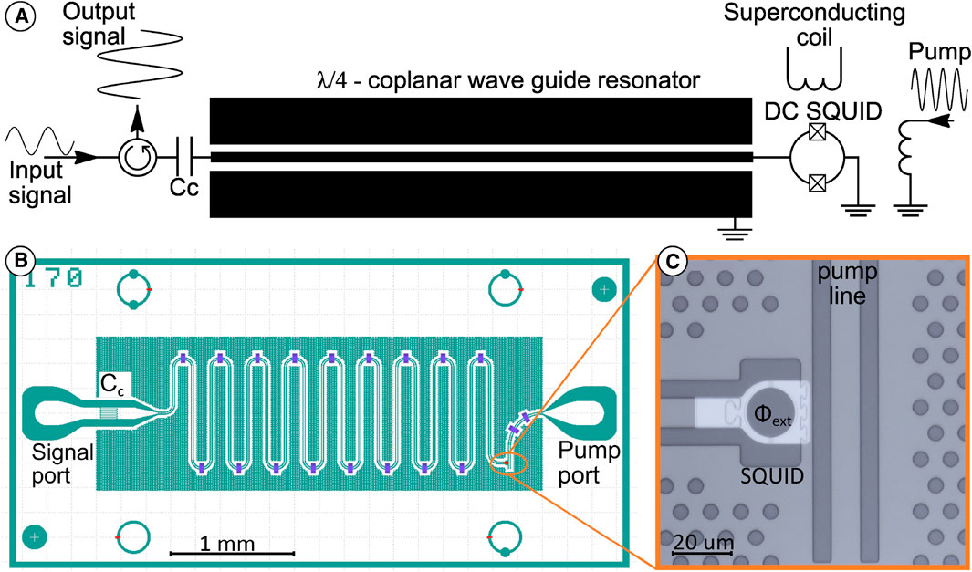
Figure 1. Flux-driven JPA. (A) Equivalent circuit diagram of the JPA. A flux bias defines the average inductance of the SQUID loop (the Josephson junctions are denoted as
Different JPAs were designed for amplifying different signal frequencies by changing the length of the
The JPA is operated in the three-wave mixing mode [36], where the frequencies of the pump
The JPA chips have dimensions of
4 JPA measurement setup
4.1 RF setup
In Figure 2, one can observe the basic setup for testing and for the axion search experiment, featuring various temperature stages, including 300 K, 4 K, still, cold plate (CP), and mixing chamber plate (MXC) of the dilution refrigerator (DR). This design is adaptable to different types of DRs and the nature of the experiment. It offers inputs for measuring various parameters such as tuning frequency range, gain, instantaneous bandwidth, and noise temperature of the JPAs. All RF connections from the 300 K flange to the 4K plate are made with CuNi coaxial 0.047-inch-diameter cables, provided either by BlueFors (BF) [38] or made in-house. Below 4K, some of the RF lines are done with the same cable, while the signal lines are constructed using KEYCOM [39] superconducting NbTi 0.047-inch-diameter cables to minimize heat load and reduce losses. Each input line is equipped with a series of attenuators, thermally anchored to each temperature stage of the fridge, to reduce Johnson noise originating from higher temperature stages. The attenuator values are chosen by considering the equation below Eq. (7):
where
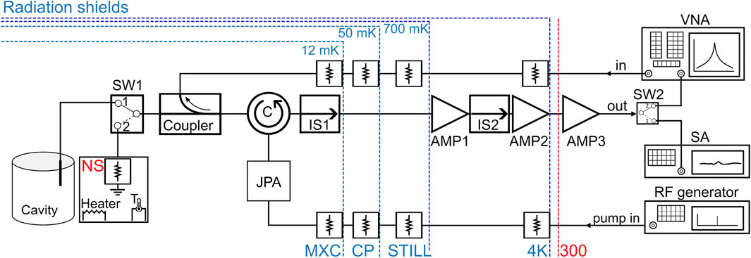
Figure 2. JPA readout diagram with either a cavity or a noise source at the input. Components arranged from left to right: noise source for tests or cavity for experiment run, SW1: RF switch to toggle between JPA-test and axion-experiment modes; the Coupler: “cold” directional coupler for injecting test signals into the JPA; components C and IS1 are a cryogenic RF-circulator and an RF isolator; AMP1 and AMP2: cryogenic HEMT amplifiers; IS2: RF isolator between HEMTs; AMP3: room temperature amplifier; SW2: RF switch between VNA and SA; VNA, SA, and RF generator.
4.2 DC wiring, cold DC filters and switch boxes
To test our JPAs and other RF and DC components, we set up a dedicated test system using a BF LD400 dry fridge [41]. To enhance our testing capabilities, we implemented a set of 32 differential lines, each individually shielded, into the fridge. These lines are constructed using twisted pairs, each placed within a Teflon matrix and equipped with its own CuNi braided shield. For pairs connecting the room temperature (RT) flange to the 4 K stage, we utilized cables with 0.1 mm diameter brass wires. For connections between the 4 K stage and the MXC, twisted pairs were made from copper nickel coated 0.1 mm NbTi wires. The cables were thermally connected to each temperature stage through their CuNi shields. On the 4 K stage, they were thermally connected via a specialized interconnection box, providing a transition between brass and superconducting wires. At a base temperature of approximately 11 mK on the MXC, the estimated maximum heat load from wires connected to the upper stage does not exceed 0.8
In the fridge DC lines, we incorporated DC filter assemblies at the 4 K stage. Each of our filter assemblies contained 12 differential T-type RC filters. In the lines used to provide power for the HEMT amplifiers, the RC filters are replaced with LC filters in order to reduce resistive losses. These filters are constructed on a two-layer PCB, utilizing both sides as ground planes to minimize interference and enhance thermalization, see (Figures 3A,B).
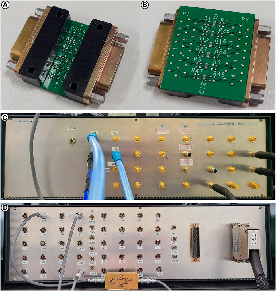
Figure 3. DC and RF wiring. (A) Top and (B) bottom views of the cryogenic filter block for the BF fridge. The block contains 12 differential T-type RC filters designed for standard BF DC lines and is mounted on the 4 K stage of the fridge. (C) DC and (D) RF boxes of the test fridge BF4 located at room temperature.
To safeguard the connectors on the top of the BF fridge from potential damage due to frequent connection and disconnection during testing, we have designed two specialized boxes for DC and RF connections (Figures 3C, D). These boxes are permanently connected to the fridge, and all connections for setup, testing, and experiments are made within these boxes. The RF box also houses an RF amplifier, while the DC box features switches controlled by a 40-411-001 PXI 64 Channel Relay Driver Module [42] based on a PXES-2590 chassis [43], enabling flexible configurations for testing purposes.
4.3 Noise source
Our setup incorporates a noise source (NS), facilitating the measurement of noise parameters for the JPAs and cryogenic HEMT amplifiers. The NS is a separate assembly comprising a wideband matched 50
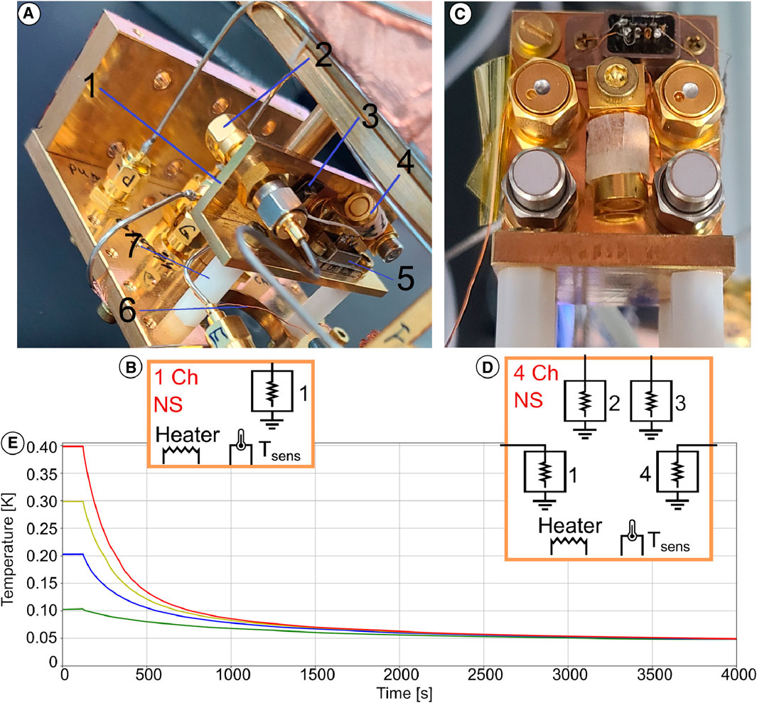
Figure 4. Cryogenic NS. (A) One-channel NS components on the MXC assembly: 1 - enclosure, 2 - 50
This NS has been designed for placement on the MXC plate of dry BF or wet Leiden dilution refrigerators. Our design prioritizes compact dimensions, minimizing the footprint on the MXC plate while ensuring adequate heat capacity for thermal stabilization. Bulkhead SMA adapters were employed to establish connections between the 50
For the interconnections between the NS and the rest of the measurement chain, we utilized 0.047-inch-diameter NbTi microwave coaxial cables. Three superconducting NbTi twisted-pair cables within braided CuNi shields were employed to connect the temperature sensor (4) and heater (3) to the micro-Sub-D-9 connector (5) of the NS. The four-point temperature measurements were conducted using a calibrated ruthenium-oxide temperature sensor. The heater was crafted using a 100
Through a proportional-integral-derivative (PID) controller, the NS temperature could be adjusted from 50 mK to 1 K without affecting the MCX plate temperature. Initially, we employed a single-channel NS in our setup. However, as our testing requirements evolved and the demand for increased testing speed became apparent, we transitioned to a four-channel NS configuration [44], all housed within a single enclosure as shown in Figure 4C. The four channel NS equivalent circuit is shown in Figure 4D. This allowed us to significantly accelerate our testing processes.
The time it takes for the temperature of the NS to stabilize depends on the heat capacitance of the NS itself, along with all the components mounted on it, and its thermal coupling to the MXC. This thermal conductance of the coupling is determined by the length and diameter of the copper magnet wire, the annealing of the wire, and the quality of the contacts between the wire, the NS enclosure on one side, and the MXC plate on the other. To ensure efficient thermal transfer, we took careful steps to establish good contacts. We removed the insulation clad from the wire and pressed the wire against the enclosure and plate using brass screws. We attempted to enhance contact reliability by introducing clamp contacts on both sides of the wires, but this approach led to a significant reduction in thermal conductivity, preventing us from lowering the temperature of our NS below about 180 mK. We attribute this to the introduction of substantial mechanical defects in the crimped connections, resulting in a significant increase in thermal resistance. A similar effect has been observed in other experiments [45]. After returning to our initial connection method, the thermal connection was restored.
In Figure 4E, the relaxation of the NS temperature after it was set to target temperatures is shown. The relaxation curve deviates from an exponential shape due to the strong non-linearity of thermal conductance and heat capacities at millikelvin temperatures.
4.4 Shielding of JPAs and RF components from magnetic fields
According to Eq. 5, the scanning speed of axion haloscope searches is strongly determined by the magnet’s strength and size, making it one of the pivotal factors in these experiments. The presence of such a magnet also generates a large magnetic field in its vicinity. Contemporary magnets incorporate compensation coils to establish a reduced magnetic field zone near the magnet. Nevertheless, the available space for this purpose is constrained by the size of the fridge. Consequently, it may not be sufficient to accommodate all sensitive components. Our superconducting magnets, which generate a magnetic field ranging from 8 to 18 T, with an aperture up to 320 mm, produces in a magnetic field strength of below 20 mT around the RF-readout components. As such, magnetic shielding is necessary.
4.4.1 RF switch shielding
Within our experimental setup, we face the challenge of potential magnetic field interference affecting a range of critical components, including circulators, isolators, HEMT amplifiers, and notably, the JPA. To surmount this challenge, we have used shielded components, like circulators and isolators. For the unshielded components that can only function in low magnetic field environments, such as RF switches (Figures 5A, B), special shields made from carbon steel S45C were implemented. The results of the shield simulation are shown in Figures 5C, D.
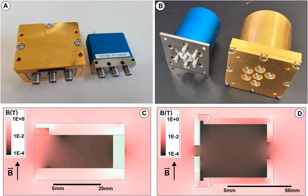
Figure 5. Two types of RF switches used at CAPP, with and without magnetic shields made from carbon steel S45C. (A) Three-position RF switch. (B) Five-position RF switch. (C) and (D) 3D simulation of the magnetic field strength in ANSYS [46] under an external vertical magnetic field of 100 mT for the three-position and five-position RF switches, respectively, are shown in the cross-sectional view.
4.4.2 Onion shield
JPAs contain the most sensitive component to magnetic fields, i.e., the SQUID. In order to safeguard them against the influence of magnetic fields, we have developed a three-layer shielding system [47], referred to as the Onion Shield (OS) due to its nested design, see Figure 6A. The performance of the OS results from its design and the properties of the materials used.
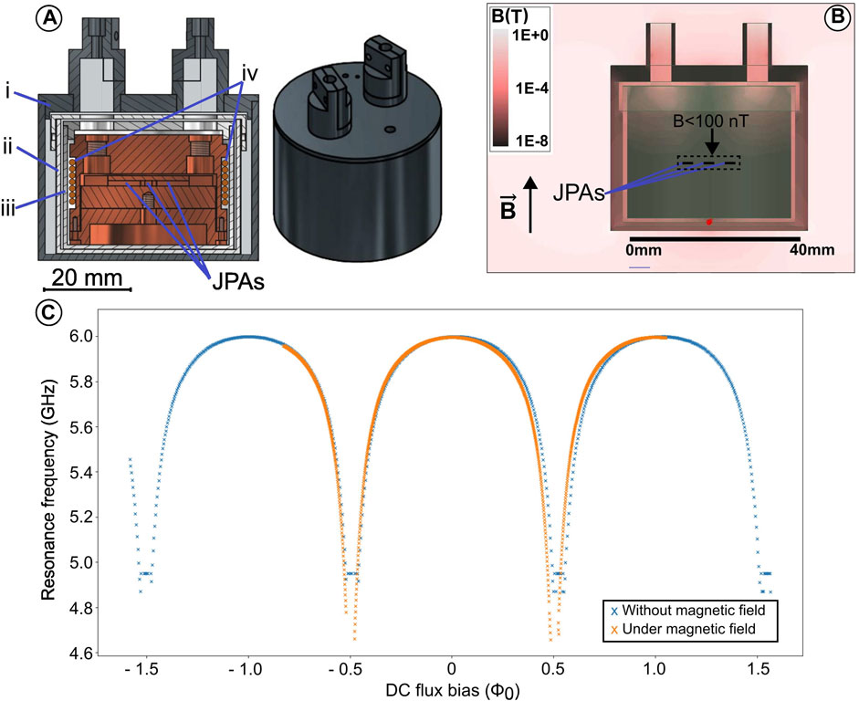
Figure 6. Onion shield. (A) Three-layer design of the shield. (I) Niobium or NbTi superconducting shield, (ii) CRYOPHY shield, (iii) inner superconducting Al shield, (iv) cross section view of the DC bias coil. The JPA locations are indicated by the arrows. (B) 3D simulation of the magnetic field in ANSYS [46], including only the two outer layers of the OS, under an external field of 50 mT and at a temperature of 100 mK. (C) Resonance frequency
The shield has three layers, each with its own function to block and control magnetic fields (Table 1). The outermost layer (1) in Figure 6A), constructed with Nb or Nb alloy superconducting materials, has a high critical magnetic field value, and the external magnetic field is shielded by it only at cryogenic temperatures. The second layer 2), consisting of a ferromagnetic material with high magnetic permeability [48, 49], shields magnetic fields penetrating the outer shield through the structural openings. Finally, the innermost layer (3) is also made of superconducting aluminum with a critical temperature of about 1.2 K.
Table 1. Onion shield layer properties.
At non-cryogenic temperatures, the OS acts like a regular magnetic shield due to its second layer made of ferromagnetic material. In fields with a magnitude close to the Earth’s field, the calculated field inside the OS is a few tens of nT. During the initial cooling, the outermost layer undergoes a superconducting transition at the critical temperature (for our material choice it is between 9.2 and 11 K). During the transition from the normal to the superconducting state, the outer layer of the OS “freezes” the Earth’s magnetic field inside the shield. Throughout this process, the magnetic field inside the second shield, composed of a ferromagnetic material, remains predominantly unaffected.
As the cooling process continues and the temperature approaches the critical point for the innermost layer 3) of the shield, its phase transition occurs. This innermost layer of the shield, made of superconducting aluminum, freezes the residual magnetic field that penetrated through the previous layers, i.e., a few tens of nT.
Since the first layer of the OS is in a superconducting state, while the field strength of the magnet increases, a persistent current appears on the surface of the first layer of the OS due to Meissner effect. This current freezes the magnetic field within this layer. However, some magnetic field penetration is inevitable through the openings required for cable routing and thermalization.
The second shielding layer plays a pivotal role in substantially reducing the penetration of the magnetic field into the first layer of the OS. However, again due to cable holes, there is a small penetration through it. This change in the residual field of the ferromagnetic shield is further shielded by the aluminum layer. Persistent currents induced on the surface of the third shield counteract minor field fluctuations within the second layer, ensuring that these fluctuations do not impact the magnetic field within the OS internal volume. Consequently, this configuration effectively shields the internal volume from the influence of external magnet field variations. The magnetic field at the location of the JPAs is approximately 50 mT when the magnet is running at 12 T. The magnetic field within the shield at this position experiences only marginal changes, even when the magnet is on, remaining within a range of 50–100 nT. This is confirmed by both simulation and experiments. Simulations in Figure 6B and measurement, in Figure 6C, showed consistent results. The measurements were done with JPA #18 (see Table 2). A more detailed investigation of the OS in fields greater than 0.1 T will be presented in a future publication.
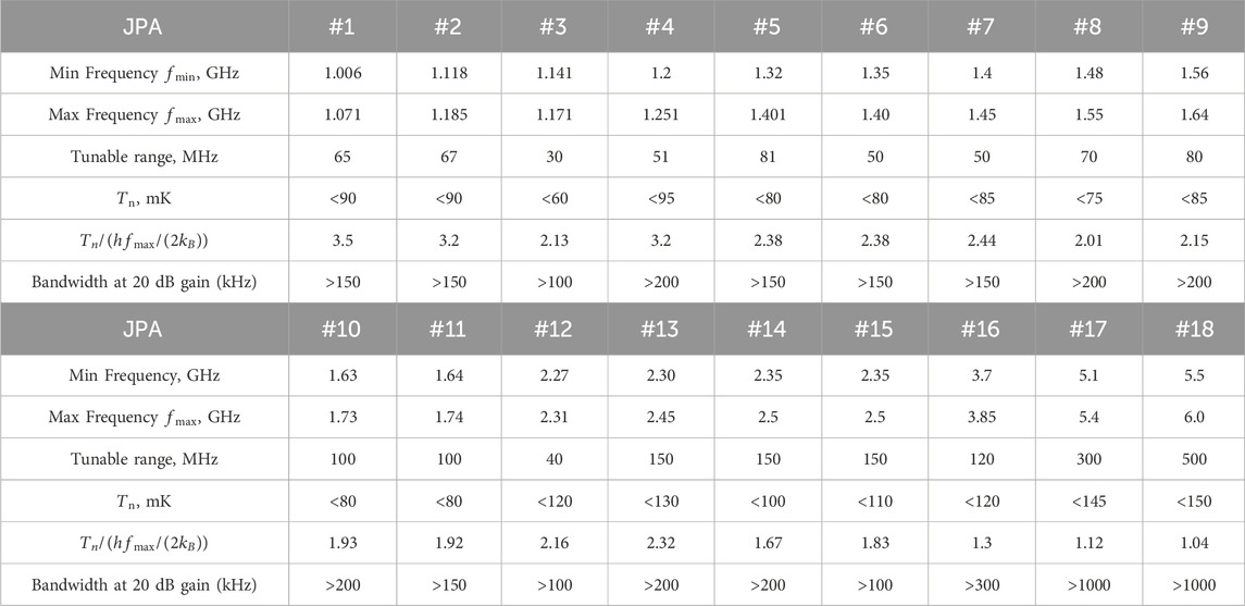
Table 2. Characteristics of some of the JPAs measured at physical temperature of 30 mK.
5 JPA characterization
For all of our devices, we conduct thorough testing procedures. Since the JPA functions as a resonant amplifier, our objectives are to determine the tunable range, explore the relationships between gain, instantaneous bandwidth, and noise as a function of pump power and detuning frequency, and establish the input signal range within which the amplifier does notsaturate. The key steps in our characterization process include.
1. Passive resonance identification by measuring the resonance frequency as a function of the DC flux.
2. Gain parametric map (paramap) construction (gain
3. The 1 dB gain compression point
4. Noise paramap generation by measuring the noise temperature
5.1 Resonance frequency vs. DC flux bias current
In the passive regime, where no pump signal is applied, the JPA operates as a weakly coupled quarter-wave resonator, shorted to ground through a non-hysteretic SQUID, and coupled to the outside circuit via a capacitor
where
The operating frequency of the JPA is determined by both the physical dimensions of the transmission line and the inductance of the SQUID. To adjust this frequency within a specific range, we utilize an inductively coupled DC flux bias coil. This coil is constructed as a single-layer coil wound with 0.05 mm copper-coated NbTi wire on a copper core, featuring an inner diameter of 32.5 mm and a length of 11.5 mm. It comprises 200 windings and has an approximate resistance of 200
The impedance of a quarter-wavelength resonator becomes finite and real at resonance, ideally zero. As a result, the reflection coefficient exhibits a dip at resonance. However, in the low loaded quality factor regime, it results in a small and broad dip spread over a wide frequency range (approximately 100–200 MHz). When measuring the JPA through various components, each with its own characteristics, distinguishing this dip becomes challenging. On the other hand, phase measurement is comparatively easier because the resonance induces a 360-degree phase shift, whereas the phase shifts of other components do not exhibit such a strong frequency dependence. For this reason, we utilize phase-frequency measurements. We examine the JPA by sending a tiny signal towards it and recording the reflected signal. To separate the incoming and outgoing waves, a circulator is employed. The signal from the JPA is then amplified using two low-noise cryogenic HEMT amplifiers, AMP1 and AMP2, and RT amplifier AMP3, see Figure 2. The output signal recorded at the VNA input is influenced by several frequency-dependent components within the chain, resulting in the observed signal profile depicted in Figure 7A. The reflection signal of the JPA is obtained through
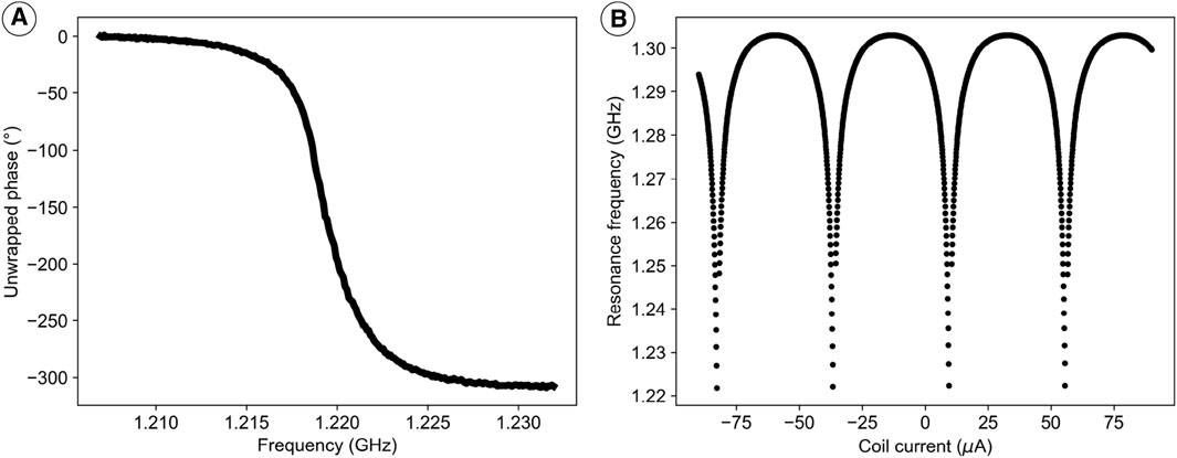
Figure 7. The passive resonance of the JPA. (A) Dependence of
The phase of reflected signal is given by Eq. 10:
Here,
5.2 JPA gain measurement
Upon applying a pump signal with frequency
Next, the JPA is tuned to the desired working point, and a subsequent transmission measurement
To find the optimal working point, we measure a “paramap”, which represents the dependence of
To determine the operational points across the entire frequency range, we devised a two-step procedure. Optimization included finding values of
During paramap measurements, after each adjustment of
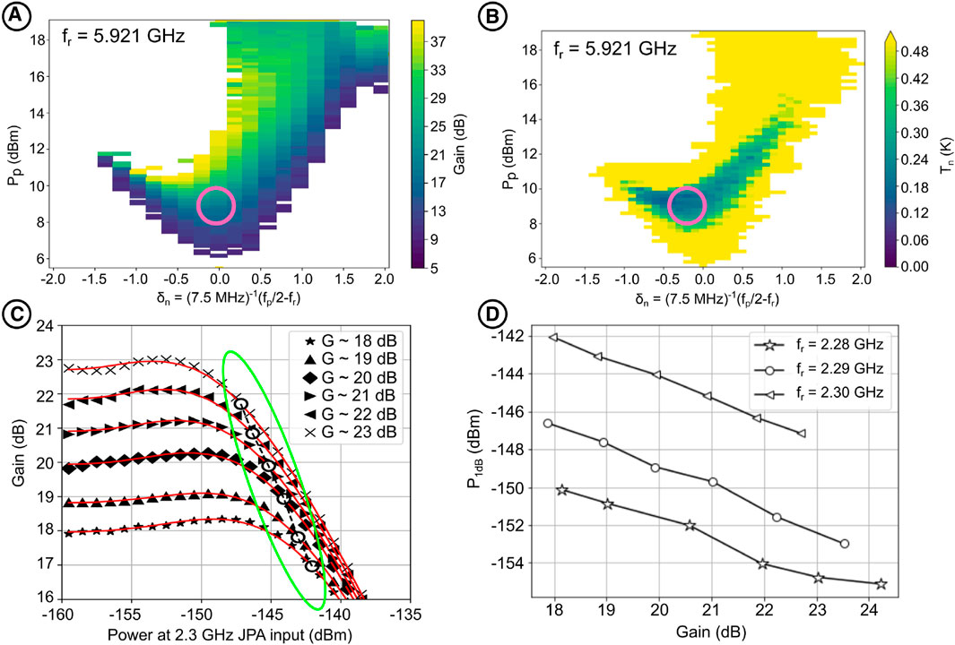
Figure 8. Characterization of the JPAs. (A) and (B) Gain and noise parameter maps of the JPA #18 for
Based on the data acquired from the gain paramap, we outlined an area of interest and measured a noise paramap (Figure 8B) within that region. The displayed gain and noise paramap are for a JPA #18. As evident, we recorded an added noise level of around 150 mK for this amplifier, slightly exceeding the quantum limit for a phase insensitive amplifier at this frequency
For each JPA, we conducted numerous measurements at different frequencies of interest to pinpoint the optimal configuration. The results presented in Figures 8C, D showcase the outcomes of noise measurements for the JPA #18 using different settings at two distinct frequencies. The red vertical lines correspond to the quantum limits for each of these frequencies. As illustrated, for each frequency, we achieved parameters that align with very low noise levels, approaching the quantum limit.
5.3 P1dB measurement
Due to the nonlinear nature of the JPA, its gain will saturate beyond certain signal and pump amplitudes. A common method for assessing amplifier saturation involves determining the output power at which the gain decreases by 1 dB. This process involves driving the amplifier with a continuous tone at the desired signal frequency and progressively raising the input power level while tracking the output power.
Our measurement of
5.4 Idler mode and added noise
In the three-wave mixing non-degenerative mode, an idler tone appears with frequency
When the input signal
At
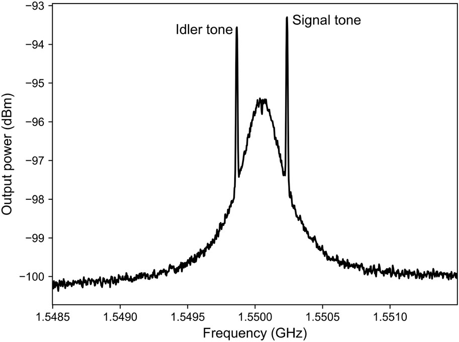
Figure 9. JPA output power measured by the spectrum analyzer including the amplified signal and its idler. A single signal tone is applied to the input of the JPA.
5.5 Noise measurement
To ascertain the noise temperature of the JPA, we utilize two steps. The first is based on the Y-factor method [56], while the second involves measuring the noise spectrum both with the JPA on and off, a technique known as the spectrum comparison method [57, 58].
5.5.1 Modified Y-factor
To measure the noise temperature, we utilized a methodology akin to the well-established Y-factor method [56], employing the NS discussed earlier in Section 4.3. The Y-factor technique is commonly applied in the field of RF and microwave measurements, particularly for evaluating the noise figure of amplifiers or receivers. It involves calculating the ratio of output noise power observed when a system is connected to a calibrated hot source (high temperature)
The right part of Eq. 14 reflects the fact that the system noise temperatures
From Eqs 14, 15, knowing
where
For illustration we considered the measurement of noise with a 2.3 GHz JPA (see Figure 10A). The noise power emerging from the system was measured with the SA with a 1 kHz resolution bandwidth. The power spectra were recorded at NS temperatures
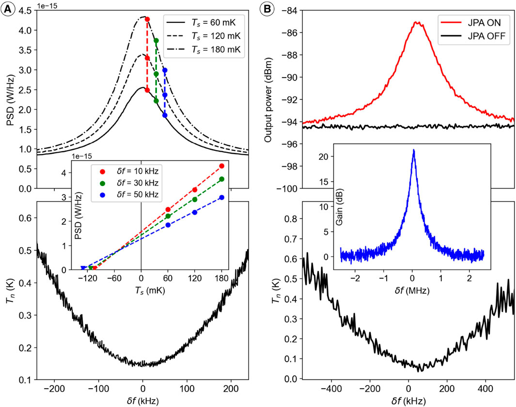
Figure 10. Noise measurements from two different JPAs: (A) JPA #12 noise measured using the Y-factor method. The upper plot shows the power spectral densities measured for
The lower limit on noise temperature for linear, phase-insensitive amplifiers is described by Eq. 17 [59]:
which results in approximately 55.2 mK at 2.3 GHz. From the measurement in Figure 10A we obtained a total added noise temperature of
5.5.2 Spectrum comparison
The second method we use in the noise measurement is the spectrum comparison method. An advantage of this method is that it does not require the continuous usage of a NS, resulting in faster measurements as there is no need for changing the temperature. This technique is applicable because the JPA can be switched on and off, allowing noise measurements in both states. The off state of the JPA corresponds to a condition where
Initially, we characterized the HEMT noise by performing the Y-factor method with the JPA turned off. For our experiments around 1 GHz the best noise we have measured with the RF-chain including HEMTs corresponds to 1 K, which is approximately 40 times the half-quanta limit.
The noise power spectrum on the output of AMP3 (see Figure 2),
As confirmed by our measurements, both methods yield results that are consistent within the measurement error. However, the spectrum comparison method allows achieving the same precision much faster. In recent experiments, we have only utilized the modified Y-factor method to measure the frequency dependence of the noise temperature of the HEMT amplifier chain. We have employed spectrum comparison methods to measure the noise of the JPA (Figure 10B).
5.6 Optimization of working point
5.6.1 Paramap optimization
Based on the JPA tests described in this section, we obtain an optimal working point (OWP) for each signal frequency
The JPA gain is a function of frequency, typically with a peak occurring at
1. Tune
2. Set
3. Increase
4. Repeat steps 2 and 3 for small deviations from
5. Pick a set of
Before running the experiment, we conduct a series of preliminary measurements to determine the optimal values of the JPA parameters
We have also devised a method to heuristically find an optimized working point using the Nelder-Mead algorithm [62]. This approach allowed us to identify a working point with a low noise temperature near a given initial seed [63].
5.7 CAPP JPA collection
Since 2019, we have designed and tested over 40 JPAs for CAPP’s axion search experiments. Parameters for some of these JPAs are presented in Table 2. The minimum operation frequency
6 Extension of amplification bandwidth
Our primary challenge stemmed from the constrained tunable range imposed by the necessity to cool down our substantial 1.2-ton magnet using liquid helium. Consequently, we opted for a wet dilution refrigerator as a key component in our experimental setup to ensure safe superconducting magnet operations. Each cooldown of the dilution refrigerator consumes several hundred liters of liquid helium, and replacing the JPA requires several weeks of effort. Therefore, it is practical to match the amplifier’s bandwidth with the cavity’s, which is approximately 300 MHz. This can be achieved by employing a split-band technique, wherein each amplifier operates within its designated frequency band.
6.1 Cold multiplexer
Initially we considered a measurement setup with a microwave RF switch as the simplest means for extending the scanning frequency range of the RF chain. The multiplexing design of the multiple JPA readout scheme was based on the five-position RF switch, shown as SW2 in Figure 5A. This way, we designed the setup, such that each channel of the RF switch is connected to the one of five JPAs, utilizing a common output, see Figure 11A. The axion signal detection chain starts from the cavity, connecting to the RF switch SW1, which is used to switch between the cavity (scanning for axions) and the noise source (noise measurements). The first directional coupler DC1 connects to the BYPASS line, which is used for the characterizing of the passive resonances of each JPA. Similar to the circuit diagram shown in Figure 2 the cryogenic circulator C1 is connected to the JPA. The five-position RF switch SW2 switches between JPAs according to the operating frequency range in axion search experiment. The pump line for each JPA utilizes a power divider PD, and the pump frequency and power are set according to the active JPA. The output of multiplexed JPA circuit is connected to the microwave isolator I and an additional directional coupler DC2. DC2 is needed to perform additional measurements of the HEMT chain, see HEMT bypass line in Figure 11A, to measure the losses in the output chain of the JPA, and to precisely characterise the noise temperature. In order to characterize the differences in transmission for each channel of the RF switch, we performed additional measurements with the circuit diagram shown in Figure 11B. We used a four channel noise source [44], shown as 4 CH NS, with 4 identical cryogenic wideband terminators connected to the five-position RF switch. The common port of the RF switch is connected to the cryogenic circulator and to the JPA. We performed measurements of the JPA noise temperature for each of the channels and did not observe any differences.
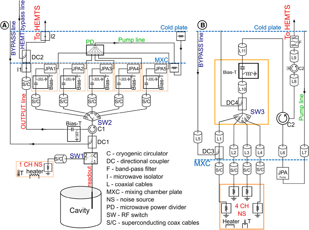
Figure 11. JPA multiplexing setup at the MXC: (A) The diagram of the detection chain in the axion search experiment. The setup consists of the cavity readout line and five JPAs measuring line. The switching is provided by the RF switch SW1. Compared with the JPA readout 2, a 5-position RF switch SW2 is added, which connects five JPAs through superconducting cables and protective bias-tees. The setup utilizes one channel noise source 1 CH NS. The pump signal is split using the power divider PD. The output is followed by an additional bias-tee, cryogenic microwave isolator I1, directional coupler DC2, and cryogenic isolator I2. (B) Setup for characterizing the transmission of each channel of the 5-position RF switch.
In our early tests, we encountered an issue where a JPA was damaged. Further investigation revealed the potential for charge accumulation on the switch electrodes during mechanical movement. This accumulated charge could discharge at the moment of switching, generating current and voltage pulses that posed a threat to the amplifiers. At mK temperatures, leakage current can be exceptionally low due to charge carriers freezing in insulating materials, resulting in prolonged charge retention on the electrodes. Once we recognized this issue, we implemented bias tees, shown as Bias-T in Figure 11A, to safely discharge the switch, enabling us to use this method for switching between several JPAs without causing damage. Another challenge associated with this method is the necessity to supply a substantial current (
6.2 Series connection of JPAs
In order to increase the bandwidth of our readout, we introduced a series connection involving an additional (see it simplified in Figure 12A) JPA alongside the first JPA (JPA1 and JPA2, see Figure 12B). During measurements, only one JPA operates at a given time, while the other JPA remains detuned from its operational frequency using a DC flux bias. This configuration seamlessly integrates into the readout chain via the second circulator, resulting in additional losses of approximately 0.4 dB at frequencies around 1 GHz. These losses, corresponding to less than 10% of the signal, lead to a minor acceptable increase in noise temperature.
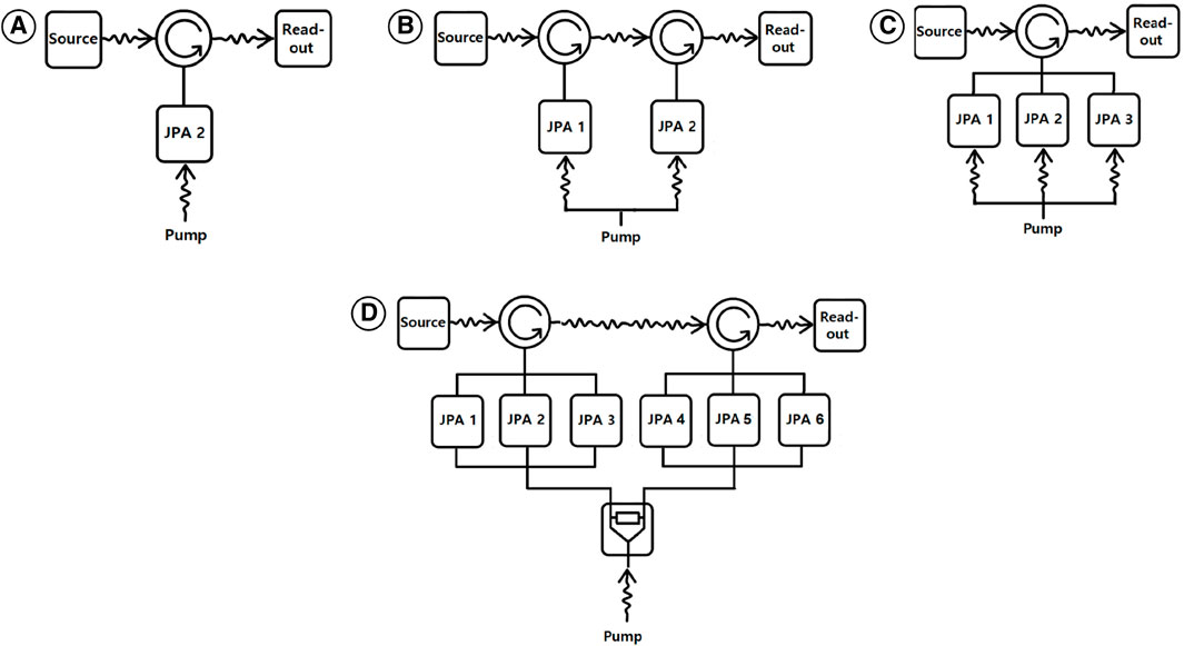
Figure 12. Simplified amplifier schematics. (A) single JPA connection, (B) serial connection, (C) parallel and (D) parallel-serial connections.
The series connection has enabled us to simultaneously use two JPAs within the same cooldown cycle, a setup we have employed in our test fridges since 2021.
6.3 Parallel connection of JPAs
The second idea for the bandwidth extension is to connect multiple JPAs with different frequencies on a single PCB, which appeared feasible given that the wavelength of the signal at 1–2 GHz significantly exceeds the length of the PCB traces of a few mm (Figure 12C). The dimensions of the PCB we use comfortably accommodate three chips, as depicted in Figure 13A.
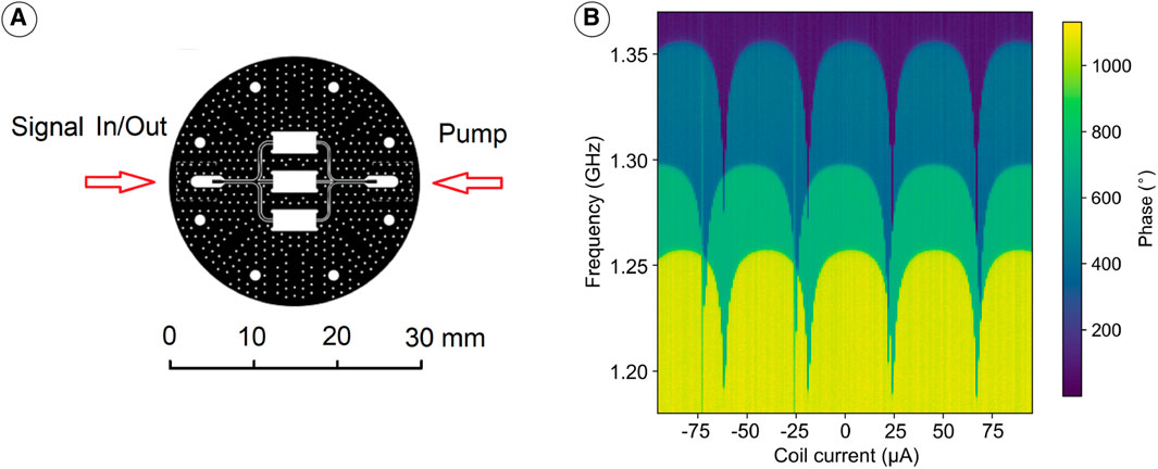
Figure 13. Parallel connection of three JPAs [37, 64, 69]. (A) PCB for the parallel connection of 3 JPAs. The DC flux bias is common for all of the JPAs and is created by a 200-turn coil wound with superconducting wire around the PCB holder (not shown). (B) Dependence of the resonance frequency on bias current for three JPAs connected in parallel, with the JPA pump switched off. Adapted with permission from ref [64] licensed under Creative Commons Attribution 4.0 International License.
The initial measurements using this parallel configuration demonstrated that the JPAs can operate independently, exhibiting noise and gain characteristics similar to those in a single-JPA operation configuration [64]. However, certain challenges may arise because the two JPAs on opposite sides of the PCB (see Figure 13A) share the same sensitivity to DC bias, causing their flux-to-frequency characteristics to change similarly. In Figure 13A, we can see three JPAs mounted on a PCB in order of their highest passive resonance frequency (HPRF): 1.28, 1.295, and 1.36 GHz. In Figure 13B, one can see the dependence of the resonance frequency on bias current for the three JPAs connected in parallel, with the JPA pump power switched off. As we can observe, there is similarity in the DC flux bias sensitivity of the JPAs with maximum resonance frequencies of 1.28 and 1.36 GHz. This similarity can potentially lead to interference in the most sensitive low-frequency range, a matter which is discussed further in Section 6.5.
6.4 Parallel-serial connection
Combining the two ideas and developing a parallel-serial JPA readout, where two parallel configurations are linked in series was the next logical step [65]. This configuration was initially evaluated in an RF assembly named “Leo-I”, which contained all RF components intended to be placed at MXC. The goal was to test the entire assembly in a dry fridge first, before moving it to the wet CAPP-MAX fridge without any modifications.
In assembly we use a magnetically shielded triple junction circulator 3CCFC11-1-MS-Sfffff custom manufactured by Ferrit-Quasar company [66]. Its first and second circulators connected to the two Orion shields and the third circulator used as an output isolator. The signal connection between NS and
In our dry testing fridge the further signal amplification is done with two LNF-LNC06
Before the dry fridge test, we arranged three JPAs in parallel with HPRFs of 1.07, 1.12, and 1.13 GHz in the first holder based on the Onion shield, while the second holder accommodated a single JPA of 1.185 GHz. Unfortunately, the middle JPA of 1.12 GHz, which was initially mounted and characterized on a single-JPA PCB version, was damaged during the transfer to the three-JPA PCB setup. Subsequent tests on the remaining three JPAs confirmed that all of them exhibited low noise levels while maintaining a required gain of 20 dB.
The complexity introduced into the readout chain led to some uneven frequency response and variations in HEMT noise temperature measured with the JPA off, ranging from 1.09 to 1.7 K (see Figures 14A, B). This cannot be entirely eliminated due to inherent phase delays in cables and the theoretical impossibility of achieving a perfect match for three-port non-reciprocal components within the chain. However, we accepted this limitation because at a JPA gain of 20 dB, the effect of the next HEMT amplification stage on noise is reduced by a factor of 100, resulting in only a small impact on the system noise temperature (Figures 14C, F).
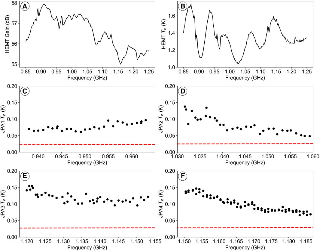
Figure 14. Characteristics of multi-JPA amplifier based on Leo I assembly. (A) HEMT amplifier gain, (B) HEMT amplifier noise. (A) and (B) were measured with all JPAs OFF. (C–F) Noise temperatures of JPAs 1–4, respectively. The red dashed line corresponds to the quantum limit for the amplifier added noise.
In Run 6 of the CAPP-MAX experiment, as mentioned earlier, three JPAs were in operation. Two of them were situated within one holder, while the third was mounted in a separate holder. The DC flux bias was shared by connecting the DC flux coils of both holders in series. Further details of the measurements conducted during Run 6 of the CAPP-MAX experiment utilizing this amplifier can be found in [37, 69].
6.5 JPA interference in split band amplifier
For Run 7 of the CAPP-MAX experiment, we prepared a new “Leo II” assembly, comprising a full set of 6 JPAs with HPRFs of 1.25, 1.30, 1.36, 1.40, 1.45, and 1.50 GHz in a parallel-serial connection as shown in Figure 12D. To minimize possible interference, we ordered the JPAs to avoid close operating frequencies among neighbors. In the first holder, we positioned JPAs starting with the lowest HPRF (1.25 GHz), followed by 1.36 GHz, and finally 1.45 GHz. The second holder followed a sequencing of 1.30 GHz, 1.40 GHz, and 1.50 GHz.
Tests of this assembly (Figure 15) in the dry fridge revealed characteristics similar to those of Leo I. These JPAs allowed us to cover a frequency range of about 300 MHz, spanning from 1.2 to 1.5 GHz. However, interference between some of the JPAs at their lowest operating frequencies emerged during testing.
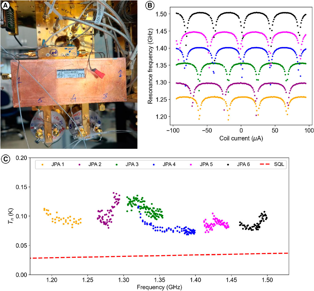
Figure 15. Six-JPA assembly (Leo II). (A) Assembly installed at the mixing chamber plate of the dry dilution refrigerator. (B) Flux-sweep curves of the six JPAs. (C) Added noise temperature depending on the frequency for the six JPAs. Each color on (B) and (C) corresponds to a JPA. The red dashed line corresponds to the quantum limit for the amplifier added noise.
This setup was tested with a series connection of DC bias lines for the two JPA holders. This configuration posed challenges, particularly in achieving detuning of the JPA resonance frequencies from each other, especially within the narrow range of the lowest operating frequencies where the sensitivity of JPAs to interference is most pronounced. Due to the use of dc bias coils with the same design and almost identical JPA flux sensitivities, leveraging the
While it would have been feasible to utilize different twisted pairs to supply DC flux bias current for the second holder, we deliberated several ideas to tackle this issue, with the objective of minimizing the interval between runs without requiring time-consuming fridge modifications.
Another approach involved connecting the DC-flux coils in parallel, with small resistors of different values in series with the coils in each branch. In this configuration, the coils will have different sensitivity to input current, but there is still a probability of interference for JPAs in different holders due to overlap at lower frequencies.
Furthermore, we developed and implemented a new circuit design using Schottky diodes. This circuit allowed us to independently apply two DC flux biases to two JPA holders using the same twisted pair of wires. It achieved this by separating the flux biases using currents of different directions to bias one or the other JPA holder. The circuit featured a diode rectifier operating at the 4 K stage of the fridge to address heat dissipation in the diodes [70].
A potential issue arose during the operation of GaAs diodes in proximity to a strong magnetic field due to the field’s effect on the diode’s performance. This effect could lead to changes in properties depending on the orientation of the diode in the magnetic field [71]. To mitigate this concern, we replaced each of the two diodes with three diodes, each oriented along different orthogonal Cartesian axes [70].
After Run 6 of our axion experiment, we re-accessed the fridge design. We decided to upgrade our DC lines and implement a twisted pair to control the second JPA holde independently. As a result, for Run 7, we were able to forego the use of this diode circuit, postponing its installation.
Before Run 7, we conducted a 6-JPA assembly (Leo-II) measurements and confirmed their noise characteristics (see Figure 15C) in the experiment fridge.
7 Conclusion
In this paper, we have presented an overview of the characterization and implementation of JPAs at CAPP, detailing the processes involved in achieving high sensitivity in axion detection. Drawing from the established flux-driven JPA technology developed by RIKEN and the University of Tokyo, we successfully adapted these amplifiers for the CAPP haloscope search experiments through several key developments.
1. We investigated and devised methods to operate flux-driven JPAs across a continuous frequency range. This involved introducing the paramap method to determine the operating points aimed at achieving specific gains and minimal noise. We established a test setup based on a dilution fridge, complemented by a computer-controlled system for JPA testing and experiment execution.
2. We introduced two methods for extending the effective amplifier frequency range, utilizing series and parallel connections. Our experiments with multiple JPA configurations, including the 6-JPA assembly, have demonstrated the efficacy of our approaches in achieving a broad frequency range. By selecting JPA sequences and employing different techniques, we successfully minimized interference and maximized sensitivity without compromising noise characteristics. By connecting 6 JPAs, each with an operating frequency band of 48–52 MHz and different central frequencies, we expanded our coverage to approximately 300 MHz, which is almost six times the range of a single JPA. It enhances our scanning capabilities by minimizing downtime and helium loss during cooldowns for the CAPP-MAX system [37].
3. We introduced a nested shield based on superconductors and CRYOPHY, enabling operation in high magnetic fields up to 0.1 T without saturating the CRYOPHY and achieving a shielding factor of
4. Our JPA development has facilitated the implementation of JPA-based amplifiers in various CAPP experiments, as described in [37, 72–76], and has allowed the CAPP to contribute to the global axion search effort.
These developments pave the way for further breakthroughs in future CAPP experiments. We also hope that our split-band amplifier technique will be a valuable tool for potential applications in other fields of study, such as basic science experiments and quantum computer readouts, extending its utility beyond its initial scope.
Data availability statement
The raw data supporting the conclusions of this article will be made available by the authors, without undue reservation.
Author contributions
SU: Conceptualization, Formal Analysis, Investigation, Methodology, Project administration, Resources, Supervision, Validation, Visualization, Writing–original draft, Writing–review and editing. JK: Data curation, Formal Analysis, Investigation, Software, Visualization, Writing–review and editing. CK: Data curation, Formal Analysis, Investigation, Methodology, Software, Validation, Visualization, Writing–review and editing. BI: Data curation, Formal Analysis, Investigation, Methodology, Validation, Visualization, Writing–review and editing. JK: Data curation, Formal Analysis, Investigation, Methodology, Software, Validation, Visualization, Writing–review and editing. AvL: Data curation, Formal Analysis, Investigation, Methodology, Validation, Visualization, Writing–review and editing. YN: Conceptualization, Formal Analysis, Funding acquisition, Investigation, Methodology, Resources, Supervision, Validation, Visualization, Writing–review and editing. SA: Data curation, Formal Analysis, Investigation, Validation, Visualization, Writing–review and editing. SO: Data curation, Investigation, Validation, Visualization, Writing–review and editing. MK: Data curation, Formal Analysis, Investigation, Visualization, Writing–review and editing. YS: Conceptualization, Funding acquisition, Project administration, Resources, Supervision, Validation, Writing–review and editing.
Funding
The author(s) declare that financial support was received for the research, authorship, and/or publication of this article. This work was supported by the Institute for Basic Science (IBS-R017-D1) and JSPS KAKENHI (Grant No. JP22H04937). AV was supported by a JSPS postdoctoral fellowship.
Acknowledgments
The authors thank Dr. Seongtae Park for his assistance with the PCB development.
Conflict of interest
The authors declare that the research was conducted in the absence of any commercial or financial relationships that could be construed as a potential conflict of interest.
Publisher’s note
All claims expressed in this article are solely those of the authors and do not necessarily represent those of their affiliated organizations, or those of the publisher, the editors and the reviewers. Any product that may be evaluated in this article, or claim that may be made by its manufacturer, is not guaranteed or endorsed by the publisher.
References
1. Du N, Force N, Khatiwada R, Lentz E, Ottens R, Rosenberg LJ, et al. Search for invisible axion dark matter with the axion dark matter experiment. Phys Rev Lett (2018) 120:151301. doi:10.1103/physrevlett.120.151301
2. Braine T, Cervantes R, Crisosto N, Du N, Kimes S, Rosenberg LJ, et al. Extended search for the invisible axion with the axion dark matter experiment. Phys Rev Lett (2020) 124:101303. doi:10.1103/physrevlett.124.101303
3. Brubaker BM, Zhong L, Gurevich YV, Cahn SB, Lamoreaux SK, Simanovskaia M, et al. First results from a microwave cavity axion search at 24 μeV. Phys Rev Lett (2017) 118:061302. doi:10.1103/physrevlett.118.061302
4. Backes KM, Palken DA, Al Kenany S, Brubaker BM, Cahn SB, Droster A, et al. A quantum enhanced search for dark matter axions. Nature (2021) 590:238–42. doi:10.1038/s41586-021-03226-7
5. Grilli di Cortona G, Hardy E, Vega JP, Villadoro G. The QCD axion, precisely. High Energ Phys. (2016) 2016(34):34–6. doi:10.1007/jhep01(2016)034
6. Wilczek F. Problem of strong p and t invariance in the presence of instantons. Phys Rev Lett (1978) 40:279–82. doi:10.1103/physrevlett.40.279
8. Kim D, Jeong J, Youn SW, Kim Y, Semertzidis YK. Revisiting the detection rate for axion haloscopes. J Cosmol Astropart Phys (2020) 2020(03):066. 066, mar 2020. doi:10.1088/1475-7516/2020/03/066
9. Sikivie P. Experimental tests of the invisible axion. Phys Rev Lett (1983) 51:1415–7. doi:10.1103/physrevlett.51.1415
10. DePanfilis S, Melissinos AC, Moskowitz BE, Rogers JT, Semertzidis YK, Wuensch WU, et al. Limits on the abundance and coupling of cosmic axions at 4.5 < ma < 5.0 μeV. Phys Rev Lett (1987) 59:839–42. doi:10.1103/PhysRevLett.59.839
12. Kim JE. Weak-interaction singlet and strong \mathrm{CP} invariance. Phys Rev Lett (1979) 43:103–7. doi:10.1103/physrevlett.43.103
13. Shifman MA, Vainshtein AI, Zakharov VI. Can confinement ensure natural CP invariance of strong interactions? Nucl Phys B (1980) 166:493–506. doi:10.1016/0550-3213(80)90209-6
14. Zhitnitsky AP. Possible suppression of axion-hadron interactions. Sov J Nucl Phys (Engl Transl.) (1980) 31(2):260.
15. Dine M, Fischler W, Srednicki M. A simple solution to the strong CP problem with a harmless axion. Phys Lett B (1981) 104:199–202. doi:10.1016/0370-2693(81)90590-6
16. Jeong J, Youn SW, Bae S, Kim D, Kim Y, Semertzidis YK. Analytical considerations for optimal axion haloscope design. J Phys G (2022) 49(5):055201. doi:10.1088/1361-6471/ac58b4
17. Jeong J, Youn SW, Bae S, Kim J, Seong T, Kim JE, et al. Search for invisible axion dark matter with a multiple-cell haloscope. Phys Rev Lett (2020) 125(22):221302. doi:10.1103/physrevlett.125.221302
18. Kwon O, Lee D, Chung W, Ahn D, Byun HS, Caspers F, et al. First results from an axion haloscope at capp around 10.7 μeV. Phys Rev Lett (2021) 126:191802. doi:10.1103/physrevlett.126.191802
19. Lownoisefactory. LNF-LNC0.6_2A (2024). Available from: https://lownoisefactory.com/product/lnf-lnc0-6_2a/ (Accessed July 16 2024).
20. Schleeh J, Alestig G, Halonen J, Malmros A, Nilsson B, Nilsson PÅ, et al. Ultralow-power cryogenic InP HEMT with minimum noise temperature of 1 K at 6 GHz. IEEE Electron Device Lett (2012) 33(5):664–6. doi:10.1109/led.2012.2187422
21. Castellanos-Beltran MA, Lehnert KW. Widely tunable parametric amplifier based on a superconducting quantum interference device array resonator. Appl Phys Lett (2007) 91(8):083509. doi:10.1063/1.2773988
22. Eom H, Day PK, LeDuc HG, Zmuidzinas J. A wideband, low-noise superconducting amplifier with high dynamic range. Nat Phys (2012) 8(8):623–7. doi:10.1038/nphys2356
23. Yaakobi O, Friedland L, Macklin C, Siddiqi I. Parametric amplification in josephson junction embedded transmission lines. Phys Rev B (2013) 87:144301. doi:10.1103/physrevb.87.144301
24. Mutus JY, White TC, Barends R, Chen Y, Chen Z, Chiaro B, et al. Strong environmental coupling in a Josephson parametric amplifier. Appl Phys Lett (2014) 104(26):263513. 07. doi:10.1063/1.4886408
25. White TC, Mutus JY, Hoi I-C, Barends R, Campbell B, Chen Y, et al. Traveling wave parametric amplifier with Josephson junctions using minimal resonator phase matching. Appl Phys Lett (2015) 106(24):242601. 06. doi:10.1063/1.4922348
26. Macklin C, O’Brien K, Hover D, Schwartz ME, Bolkhovsky V, Zhang X, et al. A near–quantum-limited josephson traveling-wave parametric amplifier. Sci (2015) 350(6258):307–10. doi:10.1126/science.aaa8525
27. Adamyan AA, de Graaf SE, Kubatkin SE, Danilov AV. Superconducting microwave parametric amplifier based on a quasi-fractal slow propagation line. J Appl Phys (2016) 119(8):083901. doi:10.1063/1.4942362
28. Miano A, Mukhanov OA. Symmetric traveling wave parametric amplifier. IEEE Trans Appl Supercond (2019) 29(5):1–6. doi:10.1109/tasc.2019.2904699
29. Urade Y, Zuo K, Baba S, Sandbo Chang CW, Nittoh K-I, Inomata K, et al. Flux-driven impedance-matched Josephson parametric amplifier with improved pump efficiency. In: APS march meeting abstracts, volume 2021 of APS meeting abstracts (2021). A28.010.
30. Lu Y-P, Zuo Q, Pan J-Z, Jiang J-L, Wei X-Y, Li Z-S, et al. An easily-prepared impedance matched josephson parametric amplifier. Chin Phys B (2021) 30(6):068504. doi:10.1088/1674-1056/ac0420
31. Giachero A, Barone C, Borghesi M, Carapella G, Caricato AP, Carusotto I, et al. Detector array readout with traveling wave amplifiers. J Appl Phys (2021) 209:658–66. doi:10.1007/s10909-022-02809-6
32. Gaydamachenko V, Kissling C, Dolata R, Zorin AB. Numerical analysis of a three-wave-mixing Josephson traveling-wave parametric amplifier with engineered dispersion loadings. J Appl Phys (2022) 132(15):154401–10. doi:10.1063/5.0111111
33. Yamamoto T, Inomata K, Watanabe M, Matsuba K, Miyazaki T, Oliver WD, et al. Flux-driven Josephson parametric amplifier. Appl Phys Lett (2008) 93(4):042510. doi:10.1063/1.2964182
34. Dolan GJ. Offset masks for lift-off photoprocessing. Appl Phys Lett (1977) 31(5):337–9. doi:10.1063/1.89690
35. Kyle M. Sundqvist and Per Delsing. Negative-resistance models for parametrically flux-pumped superconducting quantum interference devices. EPJ Quan Technol (2014) 1(1):1–21. doi:10.1140/epjqt6
36. Roy A, Devoret M. Introduction to parametric amplification of quantum signals with Josephson circuits. Comptes Rendus Physique (2016) 17(7):740–55. doi:10.1016/j.crhy.2016.07.012
37. Ahn S, Kim JM, Ivanov BI, Kwon O, Byun HS, van Loo AF, et al. Extensive search for axion dark matter over 1 GHz with CAPP’s Main Axion eXperiment. Phys Rev X (2024). arXiv:2402.12892, accepted in. doi:10.48550/arXiv.2402.12892
38. Bluefors. Enabling the future of quantum technology (2024). Available from: https://bluefors.com (Accessed July 16 2024).
39. KEYCOM. Superconducting coaxial cable assemblies (0.085"/0.047"/0.034" type NbTi-NbTi superconducting coaxial cables) (2024). Available from: https://keycom.co.jp/eproducts/upj/upj7/page.htm (Accessed July 16 2024).
40. Yokogawa. Site map (2023). Available from: https://tmi.yokogawa.com/kr/solutions/products/generators-sources/source-measure-units/gs200/ (Accessed July 16 2024).
41. Bluefors. Dilution refrigerator measurement systems (2022). Available from: https://bluefors.com/products/dilution-refrigerator-measurement-systems/ (Accessed July 16 2024).
42. Pickeringtest. 64 channel relay driver module (2024). Available from: https://www.pickeringtest.com/en-us/product/64-channel-relay-driver-module (Accessed July 16 2024).
43. Adlinktech. Products PXI PXIe platform PXIChassis PXES-2590 (2024). Available from: https://www.adlinktech.com/Products/PXI_PXIe_platform/PXIChassis/PXES-2590 (Accessed July 16 2024).
44. Ivanov BI, Kim J, Kutlu Ç, van Loo AF, Nakamura Y, Uchaikin SV, et al. Four-channel system for characterization of Josephson parametric amplifiers. In: Proc. Of the 29th international Conference on low temperature physics (LT29), pages 0112001–0112006. JPS con Proc (2023). doi:10.7566/jpscp.38.011200
46. Ansys. Ansys simulation software (2024). Available from: https://www.ansys.com/ (Accessed July 16 2024).
47. Uchaikin SV, Ivanov BI, Kim J, Kutlu Ç, van Loo AF, Nakamura Y, et al. CAPP axion search experiments with quantum noise limited amplifiers. In: Proc. Of the 29th international conference on low temperature physics (LT29). JPS Con Proc (2023). p. 0112011–6. doi:10.7566/JPSCP.38.011201
48. Aperam. Product cryophy (2024). Available from: https://www.aperam.com/product/CRYOPHY/ (Accessed July 16 2024).
49. Arpaia P, Buzio M, Capatina O, Eiler K, Langeslag SAE, Parrella A, et al. Effects of temperature and mechanical strain on ni-fe alloy cryophy for magnetic shields. J Magn Magn Mater (2019) 475:514–23. doi:10.1016/j.jmmm.2018.08.055
50. Krantz P, Reshitnyk Y, Wustmann W, Bylander J, Simon G, Oliver WD, et al. Investigation of nonlinear effects in Josephson parametric oscillators used in circuit quantum electrodynamics. New J Phys (2013) 15(10):105002. doi:10.1088/1367-2630/15/10/105002
51. Haus HA, Mullen JA. Quantum noise in linear amplifiers. Phys Rev (1962) 128:2407–13. doi:10.1103/physrev.128.2407
52. Kutlu Ç, van Loo AF, Uchaikin SV, Matlashov A, Lee D, Oh S, et al. Characterization of a flux-driven Josephson parametric amplifier with near quantum-limited added noise for axion search experiments. Supercond Sci Technol (2021) 34:085013. doi:10.1088/1361-6668/abf23b
53. Yurke B, Corruccini LR, Kaminsky PG, Rupp LW, Smith AD, Silver AH, et al. Observation of parametric amplification and deamplification in a josephson parametric amplifier. Phys Rev A (1989) 39:2519–33. doi:10.1103/physreva.39.2519
54. Kuzmin L, Likharev K, Migulin V, Zorin A. Quantum noise in josephson-junction parametric amplifiers. IEEE Trans Magn (1983) 19(3):618–21. doi:10.1109/tmag.1983.1062472
55. Babourina-Brooks E, Doherty A, Milburn GJ. Quantum noise in a nanomechanical duffing resonator. New J Phys (2008) 10(10):105020. doi:10.1088/1367-2630/10/10/105020
56. Engen GF. A new method of characterizing amplifier noise performance. IEEE Trans Instrum Meas (1970) 19(4):344–9. doi:10.1109/tim.1970.4313925
57. Friis HT. Noise figures of radio receivers. Proc IRE (1944) 32(7):419–22. doi:10.1109/jrproc.1944.232049
58. Sliwa KM, Hatridge M, Narla A, Shankar S, Frunzio L, Schoelkopf RJ, et al. Reconfigurable josephson circulator/directional amplifier. Phys Rev X (2015) 5:041020. doi:10.1103/physrevx.5.041020
59. Clerk AA, Devoret MH, Girvin SM, Marquardt F, Schoelkopf RJ. Introduction to quantum noise, measurement, and amplification. Rev Mod Phys (2010) 82:1155–208. doi:10.1103/revmodphys.82.1155
60. Caves CM. Quantum limits on noise in linear amplifiers. Phys Rev D (1982) 26:1817–39. doi:10.1103/physrevd.26.1817
61. Kutlu Ç, Ahn S, Uchaikin SV, Lee S, van Loo AF, Nakamura Y, et al. Systematic approach for tuning flux-driven Josephson parametric amplifiers for stochastic small signals. In: Proc. Of the 29th international Conference on low temperature physics (LT29), pages 0112021–0112027. JPS con. Proc. (2023). doi:10.7566/JPSCP.38.011202
62. Nelder JA, Mead R A simplex method for function minimization. Comput J (1965) 7(4):308–13. doi:10.1093/comjnl/7.4.308
63. Kim Y, Jeong J, Youn SW, Bae S, van Loo AF, Nakamura Y, et al. Parameter Optimization of Josephson Parametric Amplifiers Using a Heuristic Search Algorithm for Axion Haloscope Search. Electronics (2024) 13: 2127. doi:10.3390/electronics13112127
64. Uchaikin SV, Kim J, Ivanov BI, van Loo AF, Nakamura Y, Ahn S, et al. Improving amplification bandwidth by combining Josephson parametric amplifiers for active axion search experiments at IBS/CAPP. J Low Temp Phys (2024). doi:10.1007/s10909-024-03090-5
65. Kim J, Ko M, Uchaikin SV, Ivanov BI, van Loo AF, Nakamura Y, et al. Wideband amplification for IBS-CAPP’s axion search experiments. J Low Temp Phys (2023). doi:10.21203/rs.3.rs-3550142/v1
66. Ferrite Quasar. Available from: http://ferrite-quasar.ru/index.html.
67. Ferrite Quasar. Available from: http://ferrite-quasar.ru/products/cci/cci7e.html (Accessed July 16 2024).
68. Leiden Cryogenics BV. High end custom dilution refrigerators (2022). Available from: https://leidencryogenics.nl/ (Accessed July 16 2024).
69. Kim J, Ivanov BI, Kutlu Ç, Park S, van Loo AF, Nakamura Y, et al. Josephson parametric amplifier in axion experiments. In: Proc. Of the 29th international Conference on low temperature physics (LT29), pages 0111991–0111996. JPS con. Proc. (2023). doi:10.7566/JPSCP.38.011199
70. Ko MS, Uchaikin SV, Ivanov BI, Kim JM, Oh S, Gkika V. Expanding scanning frequency range of Josephson parametric amplifier axion haloscope readout with Schottky diode bias circuit. In: Proc. IEEE 24th international conference of young professionals in electron devices and materials (EDM) (2023). p. 810–3. doi:10.1109/EDM58354.2023.10225136
71. Sun ZG, Mizuguchi M, Manago T, Akinaga H. Magnetic-field-controllable avalanche breakdown and giant magnetoresistive effects in Goldsemi-insulating-GaAs Schottky diode. Appl Phys Lett (2004) 85(23):5643–5. doi:10.1063/1.1834733
72. Kim J, Kwon O, Kutlu Ç, Chung W, Matlashov A, Uchaikin S, et al. Near-quantum-noise axion dark matter search at CAPP around 9.5 μeV. Phys Rev Lett (2023) 130:091602. doi:10.1103/physrevlett.130.091602
73. Yi AK, Ahn S, Kutlu Ç, Kim JM, Ko BR, Ivanov BI, et al. Axion dark matter search around 4.55 μeV with Dine-Fischler-Srednicki-Zhitnitskii sensitivity. Phys Rev Lett (2023) 130:071002. doi:10.1103/physrevlett.130.071002
74. Yi AK, Ahn S, Kutlu Ç, Kim JM, Ko BR, Ivanov BI, et al. Search for the Sagittarius tidal stream of axion dark matter around 4.55 μeV. Phys Rev D (2023) 108:L021304. doi:10.1103/physrevd.108.l021304
75. Kutlu Ç, Lee S, Uchaikin SV, Ahn S, Bae S, Jeong J, et al. Search for qcd axion dark matter around 24.5 μeV using an 8-cell microwave resonant cavity haloscope and a flux-driven Josephson parametric amplifier. In: Proc. Of science,- 41st international conference on high energy physics (ICHEP2022) - astroparticle physics and cosmology, 414 (2023). doi:10.22323/1.414.0092
76. Kim Y, Jeong J, Youn SW, Bae S, Lee K, van Loo AF, et al. Experimental search for invisible axions as a test of axion cosmology around 22 μeV (2023). arXiv:2312.11003 [hep-ex].
Glossary
Keywords: axion dark matter, cavity haloscope, Josephson parametric amplifier, quantum noise limited amplifier, low temperature thermalization
Citation: Uchaikin SV, Kim J, Kutlu C, Ivanov BI, Kim J, van Loo AF, Nakamura Y, Ahn S, Oh S, Ko M and Semertzidis YK (2024) Josephson parametric amplifier based quantum noise limited amplifier development for axion search experiments in CAPP. Front. Phys. 12:1437680. doi: 10.3389/fphy.2024.1437680
Received: 24 May 2024; Accepted: 25 June 2024;
Published: 23 July 2024.
Edited by:
Frank Franz Deppisch, University College London, United KingdomReviewed by:
Toshiaki Inada, International Center for Elementary Particle Physics, The University of Tokyo, JapanTatsumi Nitta, International Center for Elementary Particle Physics, The University of Tokyo, Japan
Copyright © 2024 Uchaikin, Kim, Kutlu, Ivanov, Kim, van Loo, Nakamura, Ahn, Oh, Ko and Semertzidis. This is an open-access article distributed under the terms of the Creative Commons Attribution License (CC BY). The use, distribution or reproduction in other forums is permitted, provided the original author(s) and the copyright owner(s) are credited and that the original publication in this journal is cited, in accordance with accepted academic practice. No use, distribution or reproduction is permitted which does not comply with these terms.
*Correspondence: Sergey V. Uchaikin, dWNoYWlraW5AaWJzLnJlLmty