 L. Consiglio1*
 A. Flammini2
 A. Ianni1A. Marasciulli1G. Panella1L. Pietrofaccia1D. Sablone1R. Tartaglia1
- 1INFN LNGS, Assergi (AQ), Italy
- 2INFN Bologna, Bologna, Italy
The NUOVA OFFICINA ASSERGI (NOA) is a new facility for the production and integration of large-area silicon photodetectors operating at cryogenic temperatures. Silicon photomultipliers are proving to be a promising technology for next-generation experiments searching for rare events in underground laboratories. New photosensor technology with high performance at cryogenic temperature has been developed by Fondazione Bruno Kessler (FBK) and integrated at Laboratori Nazionali del Gran Sasso (LNGS) into large-area optical units, thus opening the frontiers toward the realization of scalable liquid argon experiments probing dark matter. The massive production of such detectors is now feasible in NOA, a clean room of 421
1 Introduction
In the last few decades, silicon photomultiplier (SiPM) detectors [1] have obtained overwhelming success and worldwide recognition in the detection of low photon fluxes due to their key features, such as low operating voltages, insensitivity to magnetic fields, robustness and reliability, high performance at cryogenic temperatures, and scalability in creating large arrays. Such characteristics make them attractive for a variety of scientific applications, such as large-scale time projection chambers (TPCs) based on noble liquids searching for rare events in extremely low background conditions. The collection of scintillation light is crucial to detecting neutrino or dark matter interactions in cryogenic environments. One of the issues with large cryogenic detectors for low background applications is the amount of radioactive contaminants in electronic components, connections, and cabling. Typically, SiPMs cover active areas of several tens of square millimeters. This means that for a large surface experiment, a huge number of devices and readout channels are in the close proximity to the detector electronics. To overcome this issue, one possibility is to group SiPMs into arrays to achieve a larger surface that could be read as a single-channel device. Since 2014, FBK (https://www.fbk.eu/it/), in synergy with LNGS, has been working on the development of SiPM arrays [2] of cryogenic photosensors [3, 4] with large aggregated output [5] and has operated successfully with high performance at cryogenic temperatures. This represents a big technological challenge, as in the case of the DarkSide-20k dark matter experiment [6], which aims to build thousands of SiPM-based optical units for an overall sensitive surface exceeding 20
2 NOA infrastructure
Born within the framework of the DarkSide-20k experiment, the NOA infrastructure is an ISO-6 clean room according to the ISO 14644-1 standard classification1, with an overall surface of 421
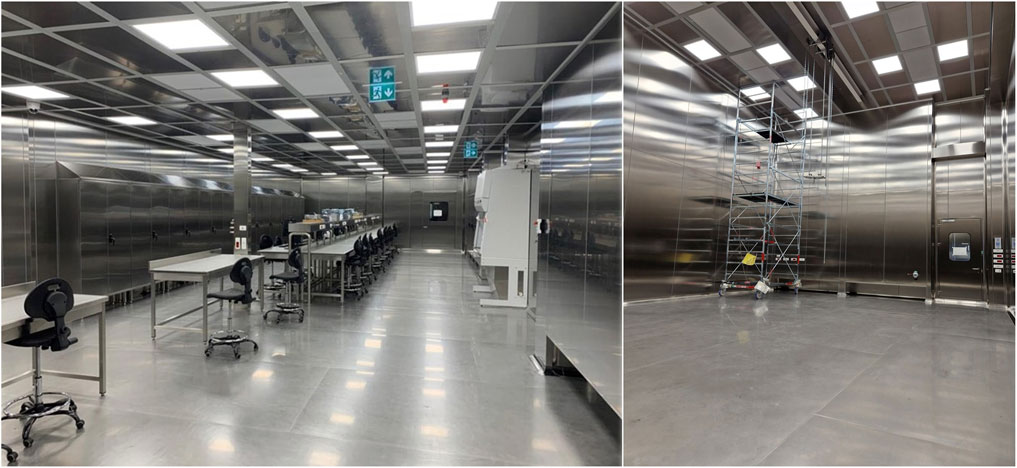
Figure 1. Left: NOA CR3 test area. Right: NOA CR2.
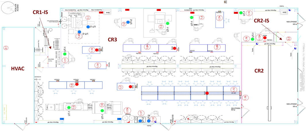
Figure 2. NOA clean room layout.
NOA CR3, with a surface area of 353
3 Production machines
The CR3 area has been equipped with sophisticated machines dedicated to the cryogenic characterization, handling, packaging, and test of large-area Si-based devices:
A part of CR3 has been devoted to the testing and characterization of the assembled devices and the related electronics: small dewars with sealed flanges, equipped with input/output and vacuum tight feedthroughs and provided with a mechanical structure to hold the devices, are available together with the related instrumentation in order to perform test measurements and data acquisition and analysis both at room temperature and in liquid nitrogen.
3.1 Cryogenic probe system
FormFactor PAC200 (Figure 3) represents a robust platform for performing electrical tests of integrated circuits at the wafer level, performing automatic testing of wafers and substrates up to 200 mm in a cryogenic environment down to 77 K. The probe plate is designed to mount a high-pin count probe card that can be thermally anchored to a cryogenic shield to reduce the heat load through the probe needles. The probe card contacts are very soft and short in length and can be numerous, depending on the specific requests. A high-resolution video microscope is mounted on a microscope movement with a travel range of 50 mm × 50 mm in the XY direction and 130 mm in the Z direction. PAC200 is equipped with a stable, vibration-isolating frame. The chuck and the motorized chuck stage, with 200 mm × 200 mm X–Y travel, theta, and Z-axis, are located inside the high-vacuum chamber. A radiation shield covers the movable chuck of the station to establish conditions of 80 K and below. Two separate cooling circuits for the shield and chuck are provided with precise temperature control that ensures stability at 0.1 K. The machine exhibits excellent measurement accuracy and repeatability.
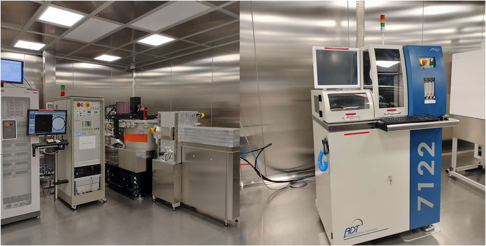
Figure 3. Left: cryogenic probe station. Right: dicer.
3.2 Dicer
ADT7122 (Figure 3) is a semi-automatic dicer system with an 8” diameter (or 200 mm × 200 mm square area) dicing area. It is an advanced, fully programmable saw for dicing thin materials into smaller pieces with 1-micron accuracy. Typical applications are Si wafer dicing, but it can also be used for other thin materials and substrates such as sapphire, glass, thin film devices, silicon, and many others with the proper choice of blade type.
3.3 Flip chip bonder
ASMPT AMICRA Nova Plus (Figure 4) is an advanced dual-head die bonding system capable of achieving placement accuracy down to few microns while bonding at temperatures exceeding 350°C and applying high bonding forces. This type of die bonding can be classified as thermo-compression bonding, and in some cases, these capabilities are required for different applications like the through-silicon vias (TSVs). Some tools of the machine have been developed for custom applications requiring the placement and bonding of large-size silicon dies (11.7 mm × 7.9 mm) on a PCB substrate using soft solder paste. A wafer magazine has been provided for die loading, while substrate loading can be done manually. The modular concept of the machine allows for enough flexibility to be upgraded to perform different processes like 3D/2.5D interconnections, TSVs, chip on chip, chip on wafer, chip on substrates, and optoelectronics.
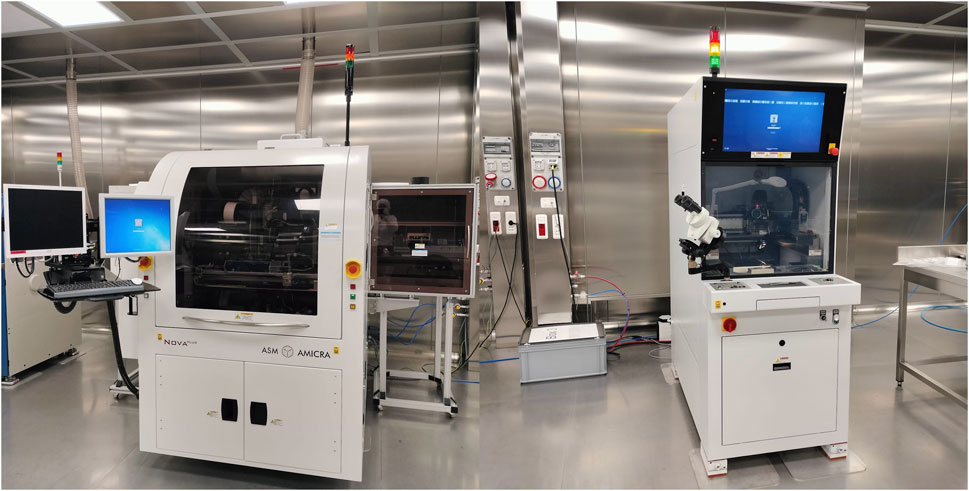
Figure 4. Left: flip chip bonder. Right: wire bonder.
3.4 Wire bonder
Bondjet BJ855 (Figure 4) is a fully automatic ultrasonic fine wedge–wedge fine wire bonder. BJ855 fulfills all wire bonding challenges on one platform. The machine is flexible and can be used with different types of bond heads (included in the machine equipment) to create bonds based on different process technologies:
Bonding wires can be positioned precisely on the large, 305 mm × 410-mm, working area. Multilevel bonding is made possible with the 32-mm Z-axis lift. Several bond stations can be placed within the working area to enable a high throughput. A permanent real-time monitoring process is in operation during the bond process, monitoring wire deformation, transducer current, frequency, and impedance within a programmable tolerance range. The system can be used in fully automatic and manual operations.
To evaluate the strength and reliability of wire bonds, a high-quality and compact pull-tester unit (LAB-Tester LT-101), equipped with most up-to-date software and available for thin and heavy wire applications, is available inside NOA.
Two microscopes with different objective magnifications are also available for optical inspection and quality control of the devices.
3.5 Semiconductor assembly systems
NOA CR3 has also been equipped with a set of semiconductor assembly systems (Figure 5) for frame film mounting, ultraviolet (UV) curing, and die expansion to handle silicon wafers.
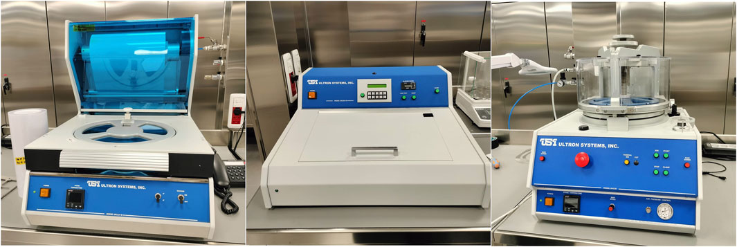
Figure 5. Manual packaging tools. From left to right: tape release, UV curing, and wafer expander.
4 Future perspectives
The NOA clean room at LNGS is a new INFN infrastructure definitively commissioned in February 2023 and designed for the production, testing, and integration of large arrays of SiPMs in a dust-controlled environment with low radon emanation. The current main user of the clean room is the DarkSide-20k collaboration, whose goal is to produce more than 500 SiPM-based photodetection units (PDUs), each sized 20 × 20 cm for an overall surface of 21
Author contributions
LC: writing–original draft. AF: writing–review and editing. AI: writing–review and editing. AM: software and writing–review and editing. LP: writing–review and editing. GP: writing–review and editing. DS: writing–review and editing. RT: writing–review and editing.
Funding
The author(s) declare that financial support was received for the research, authorship, and/or publication of this article. The authors acknowledge support from the financial funds of “Piano Operativo Nazionale 2014–2020” (PON) and “Programma di Sviluppo RESTART, Delibera CIPE 49/16,” as well as the scientific agreement between LNGS, Regione Abruzzo, and Comune dell’Aquila.
Conflict of interest
The authors declare that the research was conducted in the absence of any commercial or financial relationships that could be construed as a potential conflict of interest.
The author(s) declared that they were an editorial board member of Frontiers, at the time of submission. This had no impact on the peer review process and the final decision.
Publisher’s note
All claims expressed in this article are solely those of the authors and do not necessarily represent those of their affiliated organizations, or those of the publisher, the editors, and the reviewers. Any product that may be evaluated in this article, or claim that may be made by its manufacturer, is not guaranteed or endorsed by the publisher.
Footnotes
1Referred to the maximum particle concentration suspended in one
2The DarkSide-20k TPC optical planes will be assembled in CR2 before installation in the apparatus in the LNGS underground cavern.
References
1. Acerbi F, Gundacker S. Understanding and simulating SiPMs. Nucl Instr Methods Phys Res Section A (2019) 926:16–35. doi:10.1016/j.nima.2018.11.118
2. D’Incecco M, Galbiati C, Giovanetti GK, Korga G, Li X, Mandarano A, et al. Development of a novel single-channel, 24 cm2, SiPM-based, cryogenic photodetector. IEEE Trans Nucl Sci (2017) 65(1):591–6. doi:10.1109/tns.2017.2774779
3. Piemonte C, Ragazzoni V, Zorzi N. NUV-sensitive silicon photomultiplier technologies developed at Fondazione Bruno Kessler. Sensors (2019) 19(308):1–24. doi:10.3390/s19020308
4. Consiglio L. The cryogenic electronics for DarkSide-20k SiPM. J Instrumentation (2020) 15:1–5. doi:10.1088/1748-0221/15/05/C05063
5. Razeto A, Consiglio L. Very large SiPM arrays with aggregated output. J Instrumentation (2022) 17(P05038):1–11. doi:10.1088/1748-0221/17/05/P05038
6. DarkSide Collaboration Aalseth CE, Acerbi F, Agnes P, Albuquerque IFM, Alexander T, Alici A, et al. DarkSide-20k: a 20 tonne two-phase LAr TPC for direct dark matter detection at LNGS. The Eur Phys J Plus (2018) 133(3):131. doi:10.1140/epjp/i2018-11973-4
7. Consiglio L. The nuova officina assergi:future perspectives beyond DarkSide-20k. PoS TAUP2023 (2024) 310:1–6. doi:10.22323/1.441.0310
Keywords: clean room, silicon photomultipliers, packaging, photodetectors, cryogenics, radiopurity
Citation: Consiglio L, Flammini A, Ianni A, Marasciulli A, Panella G, Pietrofaccia L, Sablone D and Tartaglia R (2024) NUOVA OFFICINA ASSERGI: a novel infrastructure for the production of cryogenic and radiopure Si-based photodetectors. Front. Phys. 12:1433347. doi: 10.3389/fphy.2024.1433347
Received: 15 May 2024; Accepted: 08 July 2024;
Published: 14 August 2024.
Edited by:
Luca Pattavina, Gran Sasso National Laboratory (INFN), ItalyReviewed by:
Ettore Segreto, State University of Campinas, BrazilOlga Gileva, Institute for Basic Science (IBS), Republic of Korea
Copyright © 2024 Consiglio, Flammini, Ianni, Marasciulli, Panella, Pietrofaccia, Sablone and Tartaglia. This is an open-access article distributed under the terms of the Creative Commons Attribution License (CC BY). The use, distribution or reproduction in other forums is permitted, provided the original author(s) and the copyright owner(s) are credited and that the original publication in this journal is cited, in accordance with accepted academic practice. No use, distribution or reproduction is permitted which does not comply with these terms.
*Correspondence: L. Consiglio, bHVjaWEuY29uc2lnbGlvQGxuZ3MuaW5mbi5pdA==