 Michael Fiederle
 Tilo Baumbach
95% of researchers rate our articles as excellent or good
Learn more about the work of our research integrity team to safeguard the quality of each article we publish.
Find out more
PERSPECTIVE article
Front. Phys. , 30 July 2024
Sec. Radiation Detectors and Imaging
Volume 12 - 2024 | https://doi.org/10.3389/fphy.2024.1395690
This article is part of the Research Topic Pushing Frontiers - Imaging For Photon Science View all 19 articles
Compound semiconductors are playing a major role in the production of X-ray pixel detectors for the application in laboratories and beamlines at photon sources. The performance of these detectors has constantly been improved for the last decades but experiments are still limited by the properties of the detector material, especially under high flux illumination. The fast development of perovskite crystals opens the possibility for new materials to be used as highly efficient X-ray pixel detectors. The published data until now, of the transport properties, demonstrate the large potential of perovskite semiconductors. The achieved values are comparable with the ones of CdTe-based detectors. This paper presents potential perovskite-based detector materials and compares their performance with the state-of-the-art CdTe-based detectors. The perspectives of perovskite semiconductors are promising for the production of large area X-ray detectors but still some challenges remain.
During recent years the use of Hybrid Pixel Array Detectors (HPAD) has become a standard for photon detection at synchrotron storage ring and free-electron sources for certain applications like X-ray diffraction of crystalline materials and Non-Destructive Testing by Computed Tomography. It is generally accepted that photon counting detectors offer a large improvement over current detectors based on CCD cameras. Examples are the Pilatus [1], the Medipix [2] and the XPAD [3] detectors, which have been developed in various places in Europe.
Several research projects have investigated the possibilities of achieving highly efficient detector materials and thus successfully developed the technology for their use at photon sources. In this context, a large number of semiconductors have been investigated as possible sensor materials in the last 30 years, such as PbO [4], HgI2 [5], TlBr [6], GaAs [7] and Cd-based semiconductors like CdTe, Cd (Te,Se) and (Cd,Zn) Te (CZT) [8].
The common feature of these detector-materials is the dependence of the detection efficiency on the thickness of the sensor. X- and gamma-ray detectors are bulk devices in contrast to most electronic semiconductor devices. The need for a high detection efficiency defines the requirements for the material properties.
• High-Z for efficient absorption of X- and gamma-rays, especially at high photon energies >20 keV.
• High resistivity ρ for low leakage current (ρ > 108 Ω cm)
• High mobility-lifetime product μτ of both charge carrier types for an optimum mean free path length (μτ > 10–3 cm2 V−1)
• High mobility at least of one charge carrier for prompt signal formation
• Homogeneous distribution of electronic material properties on a micrometer scale for active detector areas with several cm2.
• High structural quality given by single crystalline material.
• Low defect concentration.
• Reliable contact and interconnection technology to produce hybrid pixel detectors on a micrometer scale.
• Reliable production sources and availability at a reasonable cost
So far only the Cd-based semiconductor materials fit all requirements and yield the correct performance. Thus, the detector systems using CdTe and CZT currently define the standards regarding noise (leakage current), efficiency (mobility lifetime products μτe and μτh), spatial resolution (pixel pitch) and homogeneity (defect concentrations). Since 2021 Computed Tomography systems using CdTe detectors have been installed in clinics for the application in human medicine [9].
An overview about CdTe-based pixel detectors is shown in [10] and by Gruner et al. for general perspectives for hard X-ray pixel detectors [11].
There is a growing need for large area, highly effective X-ray pixel detectors. The application of X-ray Diffraction at higher X-ray energies at light sources as well as Computed Tomography need effective pixel detectors with several cm2 active area. For instance, reducing radiation dose for operators and patients is only possible if high-Z detectors are available. This leads to enhanced diagnostics information in the medical field and applications in inspection and analysis. The commercial use of highly effective X-ray pixel detectors is still limited by the costs and availability of the semiconductor materials. Novel, radical production techniques have to be considered to use the advantages of semiconductor X-ray sensors. Fast deposition techniques used in the development of flat panel detectors could be one possibility if the required material quality can be obtained for a new semiconductor material.
Yet, up to now, the production of large area sensors based on highly efficient semiconductors has been limited. These limitations are related to the growth and fabrication processes. The production of CdTe-based semiconductors is very complex. The materials are usually produced by melt growth techniques with temperatures above 1,100°C including toxic gases and solutions. This complexity generates a limitation in the production of the material and of the devices. Therefore, alternative materials are required.
Beyond these semiconductors a new class of materials are now in the focus of scientific research, namely, the perovskite materials. The term perovskite refers to a type of mineral structure that has a specific crystallographic arrangement. The crystal structure following the formula ABX3, where A and B are positively charged ions and X is a negatively charged ion. The name “perovskite” originates from the mineral calcium titanate (CaTiO3), which was first discovered in the Ural Mountains of Russia and named after the Russian mineralogist Lev Perovski.
This material class already yields a breakthrough for the application in photovoltaic cells. The perovskite films have pushed the photovoltaics market level up by combining low-cost production with high efficiency, thus exceeding the performance of silicon-based cells and achieving a similar performance within a few years instead of decades [12]. Perovskites represent a class of materials offering tailored performance in different fields of application.
Perovskite films can be simply produced through wet chemistry and show excellent charge transport properties with mobility-lifetime products (μτ) better than 10−4 cm2/V. The requirements for X-ray detectors, for example, the high μτ and homogeneous material properties are similar to the photovoltaic cells, adding high absorption and required thickness. Recent publications already demonstrated the possibility to use perovskite for the development of X-ray detectors [13–15].
The published data of the perovskite materials [16] showed remarkable results similar to the performance of state-of-the-art of detector material such as CdTe. Using the right class of perovskites can lead to non-toxic detectors with high absorption efficiency for X-ray energies up to 120 keV. This will open the opportunity to produce large area detector systems with high efficiency and low costs with increased sustainability.
An overview of a selection of available perovskite detectors is given in the next paragraph. This will be followed by the detailed presentation of the most promising materials. The discussion will compare the performance of the selected perovskite crystals with the state-of-the-art of CdTe and CZT based pixel X-ray detectors. A summary and perspective of the new class of materials in the field of X- and gamma-ray detectors shall finalize the paper.
Perovskites represent a class of materials containing insulators and semiconductors. This paper concentrates only on the perovskite semiconductors due to their capability of direct detection of X-rays. Subdivisions are organic, e.g., Methylammonium Lead Iodide MAPbI3 and Methylammonium Lead Bromide MAPbBr3, as well as inorganic materials, like CsPbBr3 or Cs2AgBiBr6. Latest review articles [17]; [15, 18]; provide a nearly complete list of perovskite materials working either as scintillator materials or semiconductors.
The sensitivity is given by Kasap (2000) [19]. The X-ray sensitivity S of the detector is defined as the charge Q released per unit area A per unit exposure of radiation X: S = Q/AX. The Schubweg limited X-ray sensitivity S is proportional to Φ given by:
Where Wpair is the pair creation energy, q the elementary charge, αair/ρair is the mass energy-absorption coefficient of air. α, αen are the mass energy-absorption coefficient and linear attenuation coefficient of the semidocutor material, respectively.
References of the table [20–31]:
In Table 1 a selection of perovskite semiconductors is presented showing important material properties for X-ray detectors. Part of the data are taken from Lin, C.-F. et al. [15]. From Table 1 three materials have been selected representing the best compromise between material properties and available size and thickness of detector materials. These materials are the organic based perovskites MAPbI3 or MAPbBr3, the single crystalline material CsPbBr3 and the lead-free semiconductors CsAgBiBr6. The presented perovskite crystals have two different structural appearances either thin films or bulk crystals.
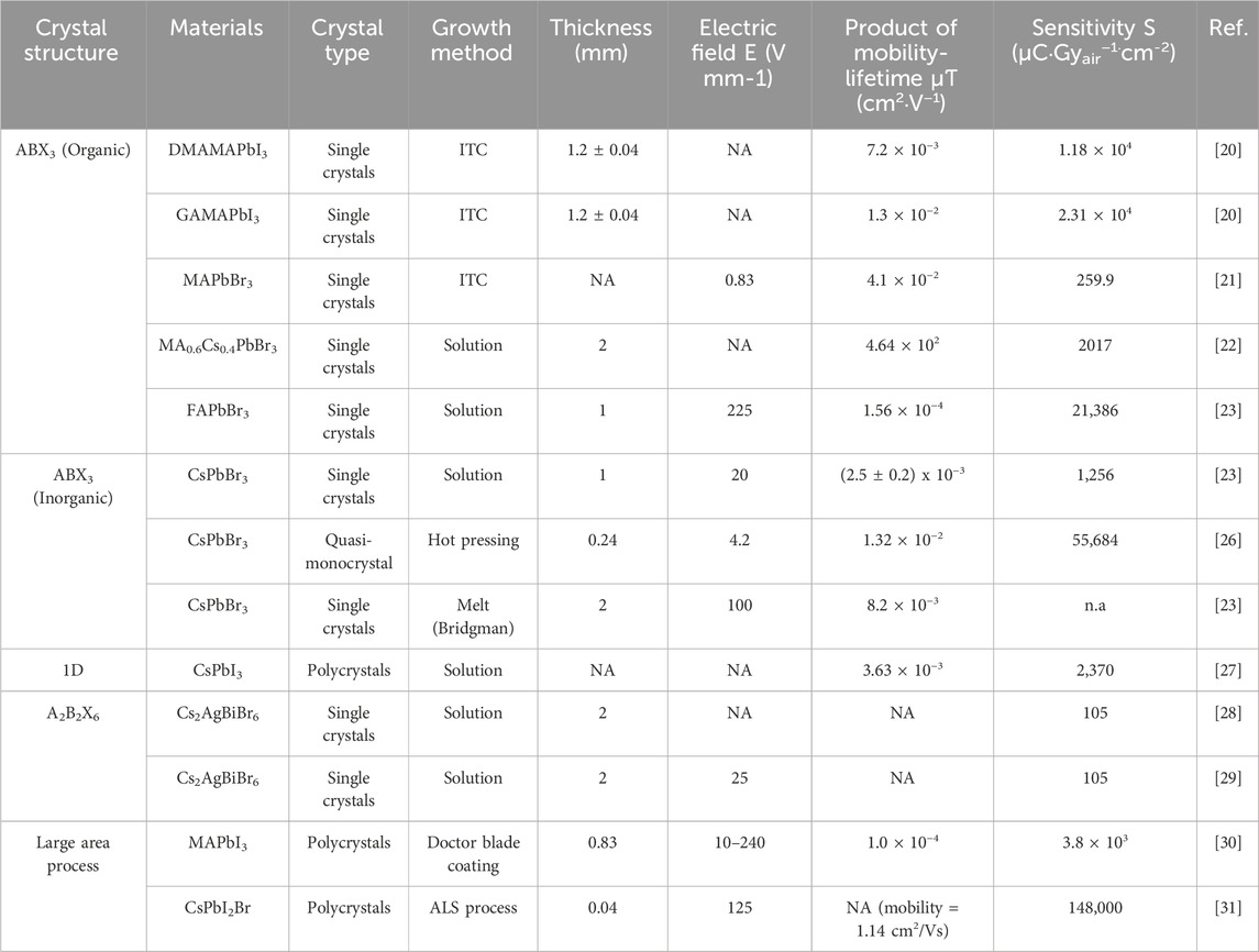
Table 1. Comparison of material properties of selected perovskite crystals.
Methylammonium lead perovskites, often referred to as MAPbX3 (X stands for a halide such as iodine, bromine, or chlorine), are a class of hybrid organic-inorganic materials that have gained significant attention in the field of photovoltaics, particularly in the development of solar cells.
The ABX3 perovskite crystals can be purely inorganic or hybrid-organic materials. The melting point are higher for the inorganic crystals, e.g., CsPbBr3 has a melting point of 567°C [32].
These perovskite materials have the chemical formula CH3NH3PbX3, where the methylammonium (MA) cation occupies the A-site, lead (Pb) occupies the B-site, and the halide (X) ions occupy the X-site in the perovskite crystal structure. The MAPbI3 is the most investigated perovskite semiconductor with applications in photovoltaic cells as well as in X-ray detectors. The production of areas up to 20 × 20 mm2 and with thickness up to 1 mm of thin films and bulk crystals is quite simple and the achieved transport properties fit the defined requirements for X-ray detectors.
The material properties of the crystals given in Table 1 demonstrate the high potential for successful X-ray detection in terms of the requirements listed above. The typical thickness is around 1 mm. The absorption efficiency can be calculated using the average Z number of the material and thickness [33]. The efficiency is close to 90 percent for absorbing 50 keV photons with a thickness of 1 mm for CsPbBr3 [34]. The MA-based perovskites yield an almost identical efficiency at 90 percent for 50 keV photons [18].
The resistivity of the intentionally undoped semiconductors is higher than 109 Ωcm, resulting in a low leakage current for applied electrical voltages up to 200 V. The most important properties are the values for the product of lifetime and mobility of the charge carriers. The multiplication of the μτ with the applied electrical field yields the mean free path length and is directly correlated with the charge collection efficiency of the detector material. The perovskite reach μτ-products of 6 × 10⁻² cm2V−1, which corresponds to a mean free path length of 12 cm for an electric field of 200 V/mm. The importance of this material property becomes apparent in comparison with conventional X-ray detector semiconductors like GaAs and CdTe. In the review article [35] the transport properties are compared to results from CdTe crystals. This comparison shows a value of 10−3 cm2/V for CdTe and several data points higher than 10−3 cm2/V for MAPI and Cs2AgBiBr6.
The crystals of these selected perovskites were produced by deposition techniques, solution growth processes as well as by melt growth method known as the Bridgman method [36]. The inverse temperature crystallization (ITC) is a solution-based process working at moderate temperature below 350°C.
In semiconductor growth, the Bridgman method is a technique used to produce high-quality single-crystal semiconductor materials. The drawback of the Bridgman method is the high growth temperature above the melting point of the material. This generates additional defects in the semiconductor.
The next paragraphs will compare perovskite crystals CsPbBr3 with state-of-the-art pixel detectors based on CdTe and CZT. In the last years remarkable results have been presented for CsPbBr3 regarding efficiency, size of detectors, and energy resolution - and therefore CsPbBr3 appears to hold the most promise for application in HPADs.
Several crystals of the perovskites fulfil the requirements for a semiconductor X-ray detector given in the first section of this paper. Several classical semiconductors fulfil these requirements as well, however, only CdTe-based materials CdTe and (Cd,Zn)Te CZT demonstrated the capability for the use as a HPAD [10]. The data are presented in Table 2.
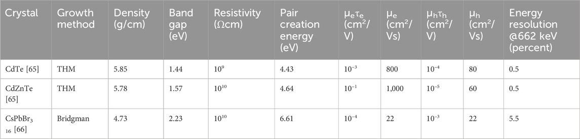
Table 2. Compares the material properties of CdTe and CdZnTe with the most promising perovskite material CsPbBr3.
The density, the bandgap, the resistivity, and the μτ-products of CsPbBr3 are comparable to the ones of CdTe and CZT. The mobility values in the table are lower and this has a strong influence on the signal formation. Consequently, the signal formation leads to a poor energy resolution. The mobilities are strongly correlated with the quality and purity of the material. Less concentration of structural defects and impurities will improve the mobilities. Z. Zhang and B. Saparov [37] collected the data of the mobilities of different perovskite crystals. Values above 100 cm2/Vs have been achieved.
However, the performance of CsPbBr3 is quite promising taking into account the few years of research applied in the field of perovskite materials. Purification processes and advanced preparation of precursor materials have just been started.
The first published paper about CdTe was in 1955 [38]. It has taken over 60 years for this material to be successfully applied as a HPAD in Human Computed Tomography scanners, in laboratories and beamlines [9–11]. These applications usually use pixel pitches between 50 μm and 250 µm. This implies homogeneous properties on the micrometer scale for active detector areas with several cm2, regarding the specified requirements from the introduction.
The success of CdTe-based detectors is controlling the concentration of structural defects and impurities. In CdTe and CZT the concentration of deep levels is relatively high. It is a very complex balance of shallow and deep levels required to obtain the high values for the μτ-products for both carrier polarities [39]. In the last decades the purification of the material and the reduction of defect concentrations are continuously improving. Nonetheless, they are still high compared to silicon but in orders of magnitude, lower than in other compound semiconductors. The concentration of the defects has a strong influence on the μτ-products for electrons and holes, respectively. Defects are electronically active and act as traps for charge carriers. They can be classified by cross sections and relaxation times.
The application for X-ray detection in modern storage rings and XFELs [40] or in Computed Tomography [41] place significantly higher demands on the material and the available technologies. One common feature is the high photon flux. In Human CT the dose rate is 6 × 10⁸ photons/mm2s. Latest publications identified a balance between the μτ-products of electrons and holes as a mandatory requirement for the applications under high photon fluxes [42]. A comparison with photon fluxes from 8 × 10⁷ photons/mm2s up to 1 × 10¹⁰ photons/mm2s given in [43] discussed the effect of after-glow with different types of materials and configurations with CdTe ohmic and Schottky contacts, GaAs, latest “high flux CZT” by Redlen and silicon p-i-n structure. In the latter device no polarization effect is visible due to very small concentration of deep levels. The edge-on geometry has been applied to increase the absorption length up to 11.4 mm and maximize the efficiency [44].
High flux applications [16] and the influence of deep levels are part of the actual research of perovskite semiconductors. At the moment the database of deep levels is small but further improvements of the electronic properties are the next logical steps. This leads to more research in the involved defects. Several papers have been published analysing the nature and influence of deep levels in perovskites:
• Thin film and bulk material are characterized by Deep Level Transient Spectroscopy DLTS as well as by Photo Induced Current Transient Spectroscopy PICTS to determine the influence on the passivation of solar cells [46] and for optoelectronic devices [47,48].
• The role of impurities is the subject of the analysis as well as the identification of native defects in publications [45,49,50].
• In Figure 1 native defects and hydrogen related deep levels are summarized with their possible levels of ionization. Figure 1 was originally published in [49].
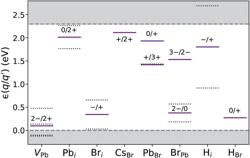
Figure 1. Thermodynamic charge state transition levels [45].
The improvement of solar cells is the main goal in the research of photo voltaic. Perovskite crystals have minimalised this breakthrough down to a few years instead of decades compared to the research of silicon-based cells in the last 50 years [12]. It can be expected that the development of X-ray detectors using perovskite semiconductors will follow a similar fast track:
The perovskite crystals are not like conventional semiconductors [51]. The remarkable data concerning the transport properties of perovskite semiconductors (see Table 1) were obtained without any additional modifications or purification procedures. The defect densities in all of these crystals are above 1013 cm-3, not counting dislocation densities [52]. Theoretical studies like in [53] and experimental data provided in [54] describe a “self-regulation” phenomenon. Siekmann et al. [55], as well as Brandt et al. [56], use the term “defect tolerance” to explain the excellent transport properties. The phenomenon of this “defect tolerance” is described as the higher energetically probability of the formation of structural defects into shallow levels instead of deep levels [57, 58]. This notion is mainly used to explain the excellent performance of halide perovskites in optoelectronic applications. One paper [59] identified the formation of antisite defects in CsPbI3. These deep levels were not effective nonradiative recombination centers. The negative influence on the transport properties were neglectable. A recent view by X. Wang et al. [60] summarizes the formation of intraband levels by extrinsic interstitials and vacancies and an electrical behavior of shallow levels.
In the perovskite semiconductors the influence of structural defects and impurities is small. It should be easier to improve the transport properties. The concentration of defects must not be reduced like in CdTe or GaAs semiconductors.
A similar situation is known by the performance of GaN-based LEDs. In GaN the dislocation density is typically above 107 1/ cm2 and the material can be used for application as a LED [61]. In GaAs the dislocation density has to be lower than 104 1/cm2 for a working LED.
The measurement of dislocation density is a suitable analysis of defect concentration in a semiconductor. Dislocations are structural defects and can mostly be correlated with grain boundaries and impurities. The dislocation density is a measure of the number of dislocations in a unit volume of a crystalline material. It means the total length of all dislocation lines per unit of volume in a crystalline solid. The dislocations can be visualized by chemical etching. A count of the number of etch pits per unit area on the etched surface defines the dislocation density.
The actual research community is still focused on the development of materials. Several presentations of pixel detectors are quite convincing but the level of the device technology is still in development [62].
The experience in the research of CdTe-based detectors will be very useful to shorten the duration to develop the perovskite crystals. The process of crystal growth and material improvement have to be finalized before the development of technology. The concept of doping and controlling of shallow and deep levels can be applied to perovskite materials to face the challenges like the ion migration and stability of contacts. These issues are strongly correlated to the quality of the material. For example, the ion migration was successfully inhibited by co-doping of extrinsic interstitials [63] and by using chenodeoxycholic acid additive [23].
Future research of perovskite-based X-ray pixel detectors should be focused on the development of the material. Reduction of impurities and defects will increase the mobilities. Higher mobilities will yield increased μ-τ-products, and thus we expect significantly improved energy resolution to be achievable with better quality crystals. This will solve most of the described challenges and will open new technologies for the production of large area pixel detectors. It would be possible to use the advantages of high-Z semiconductors with reasonable costs.
The original contributions presented in the study are included in the article/Supplementary Material, further inquiries can be directed to the corresponding author.
MF: Writing–review and editing, Writing–original draft. TB: Writing–review and editing, Writing–original draft.
The author(s) declare that financial support was received for the research, authorship, and/or publication of this article. The research was supported by the German Federal Ministry of Education and Research (BMBF) under the funding code (Förderkennzeichen) 05K22VFA.
The authors declare that the research was conducted in the absence of any commercial or financial relationships that could be construed as a potential conflict of interest.
All claims expressed in this article are solely those of the authors and do not necessarily represent those of their affiliated organizations, or those of the publisher, the editors and the reviewers. Any product that may be evaluated in this article, or claim that may be made by its manufacturer, is not guaranteed or endorsed by the publisher.
1. Dectris Home. Dectris (2024). Available from: http://www.dectris.com/(Accessed February 28, 2024).
2. CERN Accelerating Science. Medipix (2024). Available from: https://medipix.web.cern.ch/home (Accessed February 28, 2024).
3. Pangaud P, Basolo S, Boudet N, Berar JF, Chantepie B, Delpierre P, et al. XPAD3: a new photon counting chip for X-ray CT-scanner. Nucl Instrum Methods Phys Res A (2007) 571(1–2):321–4. doi:10.1016/j.nima.2006.10.092
4. Simon M, Ford RA, Franklin AR, Grabowski SP, Menser B, Much G, et al. PBO as direct conversion X-ray detector material. In: SPIE Proceedings (2004). San Diego, CA, USA.
5. Schieber M. Fabrication of HgI2 nuclear detectors. Nucl Instr Methods (1977) 144(3):469–77. doi:10.1016/0029-554x(77)90011-8
6. Hitomi K, Tada T, Kim S, Wu Y, Tanaka T, Shoji T, et al. Recent development of tlbr gamma-ray detectors. IEEE Trans Nucl Sci (2011) 58(4):1987–91. doi:10.1109/tns.2011.2123115
7. Tyazhev AV, Budnitsky D, Koretskay O, Novikov V, Okaevich L, Potapov A, et al. GaAs radiation imaging detectors with an active layer thickness up to 1mm. Nucl Instrum Methods Phys Res A (2003) 509(1–3):34–9. doi:10.1016/s0168-9002(03)01545-6
8. Fiederle M, Ebling D, Eiche C, Hofmann D, Salk M, Stadler W, et al. Comparison of CdTe, Cd0.9Zn0.1Te and CdTe0.9Se0.1 crystals: application for γ- and X-ray detectors. J Cryst Growth (1994) 138(1–4):529–33. doi:10.1016/0022-0248(94)90863-x
9. Lell M, Kachelrieß M. Computed tomography 2.0. Invest Radiol (2023) 58(8):587–601. doi:10.1097/rli.0000000000000995
10. Fiederle M, Procz S, Hamann E, Fauler A, Fröjdh C. Overview of GaAs und CdTe pixel detectors using Medipix Electronics. Cryst Res Technol (2020) 55(9). doi:10.1002/crat.202000021
11. Gruner SM, Carini G, Miceli A. Considerations about future hard X-ray area detectors. Front Phys (2023) 11:1285821. doi:10.3389/fphy.2023.1285821
12. National Renewable Energy Laboratory (NREL). Best research-cell efficiency chart (2024). Available from: https://www.nrel.gov/pv/cell-efficiency.html.
13. Li Z, Zhou F, Yao H, Ci Z, Yang Z, Jin Z. Halide perovskites for high-performance X-ray detector. Mater Today (2021) 48:155–75. doi:10.1016/j.mattod.2021.01.028
14. He Y, Wang Z, Wang Z, Dun GH, Geng X, Wang C, et al. Perovskite band engineering for high-performance X-ray detection. Front Phys (2023) 11:1114242. doi:10.3389/fphy.2023.1114242
15. Lin C-F, Huang K-W, Chen Y-T, Hsueh S L, Li M-H, Chen P, et al. Perovskite-based X-ray detectors. Nanomaterials (2023) 13:2024. doi:10.3390/nano13132024
16. Pan L, He Y, Klepov VV, De Siena MC, Kanatzidis MG. Perovskite CsPbBr3 single crystal detector for high flux X-ray photon counting. IEEE Trans Med Imaging (2022) 41(11):3053–61. doi:10.1109/TMI.2022.3176801
17. Basiricò L, Ciavatti A, Fraboni B. Solution-Grown organic and perovskite x-ray detectors: a new paradigm for the direct detection of ionizing radiation. Adv Mater Tech (2020) 6(1). doi:10.1002/admt.202000475
18. Wang Y, Lou H, Yue CY, Lei XW. Applications of halide perovskites in X-ray detection and imaging. CrystEngComm (2022) 24:2201–12. doi:10.1039/d1ce01575c
19. Kasap SO. X-ray sensitivity of photoconductors: application to stabilized A-SE. J Phys D: Appl Phys (2000) 33(21):2853–65. doi:10.1088/0022-3727/33/21/326
20. Huang Y, Qiao L, Jiang Y, He T, Long R, Yang F, et al. A-site cation engineering for highly efficient MAPbI3 single-crystal x-ray detector. Angew Chem Int Edition (2019) 58(49):17834–42. doi:10.1002/anie.201911281
21. Geng X, Feng Q, Zhao R, Hirtz T, Dun G, Yan Z, et al. High-quality single crystal perovskite for highly sensitive X-ray detector. IEEE Electron Device Lett (2020) 41(2):256–9. doi:10.1109/led.2019.2960384
22. Fan Z, Liu J, Zuo W, Liu G, He X, Luo K, et al. Mixed-cation MAxCs1−xPbBr3 perovskite single crystals with composition management for high-Sensitivity X-Ray Detection. physica status solidi (RRL) – Rapid Res Lett (2020) 14(10). doi:10.1002/pssr.202000226
23. Jiang W, Ren J, Li H, Liu D, Yang L, Xiong Y, et al. Improving the performance and high-field stability of FAPbBr3 single crystals in x-ray detection with Chenodeoxycholic acid additive. Small Methods (2023) 7(4):e2201636. doi:10.1002/smtd.202201636
24. He Y, Petryk M, Liu Z, Chica DG, Hadar I, Leak C, et al. CsPbBr3 perovskite detectors with 1.4% energy resolution for high-energy γ-Rays. Nat Photon (2020) 15(1):36–42. doi:10.1038/s41566-020-00727-1
25. Zhang H, Wang F, Lu Y, Sun Q, Xu Y, Zhang BB, et al. High-sensitivity X-ray detectors based on solution-grown caesium lead bromide single crystals. J Mater Chem C (2020) 8(4):1248–56. doi:10.1039/c9tc05490a
26. Pan W, Yang B, Niu G, Xue K, Du X, Yin L, et al. Hot-pressed CsPbBr3 quasi-monocrystalline film for sensitive direct X-ray detection. Adv Mater (2019) 31(44):e1904405. doi:10.1002/adma.201904405
27. Zhang B-B, Liu X, Xiao B, Hafsia AB, Gao K, Xu Y, et al. High-performance X-ray detection based on one-dimensional inorganic halide perovskite CsPbI3. The J Phys Chem Lett (2019) 11(2):432–7. doi:10.1021/acs.jpclett.9b03523
28. Steele JA, Pan W, Martin C, Keshavarz M, Debroye E, Yuan H, et al. Photophysical pathways in highly sensitive Cs2AgBiBr6 double-perovskite single-crystal x-ray detectors. Adv Mater (2018) 30(46):e1804450. doi:10.1002/adma.201804450
29. Pan W, Wu H, Luo J, Deng Z, Ge C, Chen C, et al. Cs2AgBiBr6 single-crystal X-ray detectors with a low detection limit. Nat Photon (2017) 11(11):726–32. doi:10.1038/s41566-017-0012-4
30. Kim YC, Kim KH, Son DY, Jeong DN, Seo JY, Choi YS, et al. Printable organometallic perovskite enables large-area, low-dose X-ray imaging. Nature (2017) 550(7674):87–91. doi:10.1038/nature24032
31. Qian W, Xu X, Wang J, Xu Y, Chen J, Ge Y, et al. An aerosol-liquid-solid process for the general synthesis of halide perovskite thick films for direct-conversion X-ray detectors. Matter (2021) 4(3):942–54. doi:10.1016/j.matt.2021.01.020
32. Kanak A, Kopach O, Kanak L, Levchuk I, Isaiev M, Brabec CJ, et al. Melting and crystallization features of CsPbBr3 perovskite. Cryst Growth Des (2022) 22(7):4115–21. doi:10.1021/acs.cgd.1c01530
33. NIST Standard Reference Database (XGAM). XCOM: photon cross sections database (2024). Available from: https://www.nist.gov/pml/xcom-photon-cross-sections-database.
34. He Y, Hadar I, De Siena MC, Klepov VV, Pan L, Chung DY, et al. Sensitivity and detection limit of spectroscopic-grade perovskite CsPbBr3 crystal for hard x-ray detection. Adv Funct Mater (2022) 32(24). doi:10.1002/adfm.202112925
35. Wu H, Ge Y, Niu G, Tang J. Metal halide perovskites for X-ray detection and imaging. Matter (2021) 4(1):144–63. doi:10.1016/j.matt.2020.11.015
36. Wang X, Zhao D, Qiu Y, Huang Y, Wu Y, Li G, et al. PIN diodes array made of perovskite single crystal for X-Ray Imaging. physica status solidi (RRL) – Rapid Res Lett (2018) 12(10). doi:10.1002/pssr.201800380
37. Zhang Z, Saparov B. Charge carrier mobility of metal halide perovskites: from Fundamentals to Ionizing Radiation Detection. In: Metal-halide perovskite semiconductors (2023). p. 89–109. doi:10.1007/978-3-031-26892-2_6
38. Kröger FA, de Nobel D. XXIV. preparation and electrical properties of CdTe single crystals. J Electronics Control (1955) 1(2):190–202. doi:10.1080/00207215508961407
39. Fiederle M, Eiche C, Salk M, Schwarz R, Benz KW, Stadler W, et al. Modified compensation model of CdTe. J Appl Phys (1998) 84(12):6689–92. doi:10.1063/1.368874
40. Graafsma H, Becker J, Gruner SM. Integrating hybrid area detectors for storage ring and free-electron laser applications. In: Synchrotron light sources and free-electron lasers (2020). p. 1225–55. doi:10.1007/978-3-030-23201-6_37
41. Bhattarai M, Bache S, Abadi E, Samei E. Exploration of the pulse pileup effects in a clinical CdTe-based photon-counting computed tomography. Med Phys (2023) 50(11):6693–703. doi:10.1002/mp.16671
42. Veale MC, Angelsen C, Booker P, Coughlan J, French MJ, Hardie A, et al. Cadmium zinc telluride pixel detectors for high-intensity X-ray imaging at Free Electron Lasers. J Phys D: Appl Phys (2018) 52(8):085106. doi:10.1088/1361-6463/aaf556
43. Greiffenberg. High-Z sensors for synchrotron sources and FELs; ‘room temperature semiconductor detectors conference 2023’. In: 2023 IEEE Nuclear Science Symposium, medical imaging conference and international symposium on room-temperature semiconductor detectors (NSS MIC RTSD); November 4–11, 2023; Vancouver, Canada. IEEE (2023).
44. Yan T, Yang C, Cui X. An edge-on energy-resolved X-ray semiconductor detector. Solid State Commun (2021) 332:114339. doi:10.1016/j.ssc.2021.114339
45. Bao C, Gao F. Physics of defects in metal halide perovskites. Rep Prog Phys (2022) 85(9):096501. doi:10.1088/1361-6633/ac7c7a
46. Ren X, Zhang B, Zhang L, Wen J, Che B, Bai D, et al. Deep-level transient spectroscopy for effective Passivator selection in perovskite solar cells to attain high efficiency over 23%. ChemSusChem (2021) 14(15):3182–9. doi:10.1002/cssc.202100980
47. Luo D, Li X, Dumont A, Yu H, Lu Z. Recent progress on perovskite surfaces and interfaces in optoelectronic devices. Adv Mater (2021) 33(30):e2006004. doi:10.1002/adma.202006004
48. Armaroli G, Maserati L, Ciavatti A, Vecchi P, Piccioni A, Foschi M, et al. Photoinduced current transient spectroscopy on metal halide perovskites: electron trapping and Ion Drift. ACS Energ Lett (2023) 8(10):4371–9. doi:10.1021/acsenergylett.3c01429
49. Swift MW, Lyons JL. Deep levels in cesium lead bromide from native defects and hydrogen. J Mater Chem A (2021) 9(12):7491–5. doi:10.1039/d0ta11742k
50. Levine I, Vera OG, Kulbak M, Ceratti DR, Rehermann C, Márquez JA, et al. Deep defect states in wide-band-gap ABX3 halide perovskites. ACS Energ Lett (2019) 4(5):1150–7. doi:10.1021/acsenergylett.9b00709
51. Yin W-J, Shi T, Yan Y. Unusual defect physics in CH3NH3PBI3 perovskite solar cell absorber. Appl Phys Lett (2014) 104(6). doi:10.1063/1.4864778
52. Le Corre VM, Duijnstee EA, El Tambouli O, Ball JM, Snaith HJ, Lim J, et al. Revealing charge carrier mobility and defect densities in metal halide perovskites via space-charge-limited current measurements. ACS Energ Lett (2021) 6(3):1087–94. doi:10.1021/acsenergylett.0c02599
53. Walsh A, Scanlon DO, Chen S, Gong XG, Wei SH. Self-regulation mechanism for charged point defects in hybrid halide perovskites. Angew Chem (2014) 127(6):1811–4. doi:10.1002/ange.201409740
54. Yao Z, Xu Z, Zhao W, Zhang J, Bian H, Fang Y, et al. Enhanced efficiency of inorganic CsPbI3−xBrx perovskite solar cell via self-regulation of antisite defects. Adv Energ Mater (2021) 11(23). doi:10.1002/aenm.202100403
55. Siekmann J, Ravishankar S, Kirchartz T. Apparent defect densities in halide perovskite thin films and single crystals. ACS Energ Lett (2021) 6(9):3244–51. doi:10.1021/acsenergylett.1c01449
56. Brandt RE, Poindexter JR, Gorai P, Kurchin RC, Hoye RLZ, Nienhaus L, et al. Searching for “defect-tolerant” photovoltaic materials: combined theoretical and experimental screening. Chem Mater (2017) 29(11):4667–74. doi:10.1021/acs.chemmater.6b05496
57. Kim G, Petrozza A. Defect tolerance and intolerance in metal-halide perovskites. Adv Energ Mater (2020) 10(37). doi:10.1002/aenm.202001959
58. Kim J, Chung C-H, Hong K-H. Understanding of the formation of shallow level defects from the intrinsic defects of lead tri-halide perovskites. Phys Chem Chem Phys (2016) 18(39):27143–7. doi:10.1039/c6cp02886a
59. Zhang X, Turiansky ME, Van de Walle CG. Correctly assessing defect tolerance in halide perovskites. The J Phys Chem C (2020) 124(11):6022–7. doi:10.1021/acs.jpcc.0c01324
60. Wang X, Zhang M, Hou T, Sun X, Hao X. Extrinsic interstitial ions in metal halide perovskites: a Review. Small (2023) 19(46):e2303060. doi:10.1002/smll.202303060
61. Li C, Xu L. The dislocation density of gan led epitaxial films grown on si substrates characterized by x - ray diffraction. In: 2020 7th International Conference on Information Science and Control Engineering (ICISCE) (2020).
62. He Z. Pixelated CsPbBr3 semiconductor gamma spectrometers, ‘room temperature semiconductor detectors conference 2023. In: 2023 IEEE Nuclear Science Symposium, medical imaging conference and international symposium on room-temperature semiconductor detectors (NSS MIC RTSD), Vancouver, BC, November 4–11, 2023 (IEEE) (2023).
63. Zhao Y, Yavuz I, Wang M, Weber MH, Xu M, Lee JH, et al. Suppressing ion migration in metal halide perovskite via interstitial doping with a trace amount of multivalent cations. Nat Mater (2022) 21(12):1396–402. doi:10.1038/s41563-022-01390-3
64. Suzuki K, Shiro A, Toyokawa H, Saji C, Shobu T. Double-exposure method with synchrotron white X-ray for stress evaluation of coarse-grain materials. Quan Beam Sci (2020) 4(3):25. doi:10.3390/qubs4030025
65. Zappettini A. Cadmium telluride and cadmium zinc telluride. In: Single crystals of electronic materials (2019). p. 273–301. doi:10.1016/b978-0-08-102096-8.00008-2
Keywords: X-ray detectors, high-Z semiconductors, perovskites, pixel detectors, synchrotron detectors
Citation: Fiederle M and Baumbach T (2024) Perspective of perovskite-based X-ray hybrid pixel array detectors. Front. Phys. 12:1395690. doi: 10.3389/fphy.2024.1395690
Received: 04 March 2024; Accepted: 21 June 2024;
Published: 30 July 2024.
Edited by:
Cornelia B. Wunderer, Helmholtz Association of German Research Centres (HZ), GermanyReviewed by:
Pietro Zambon, Dectris AG, SwitzerlandCopyright © 2024 Fiederle and Baumbach. This is an open-access article distributed under the terms of the Creative Commons Attribution License (CC BY). The use, distribution or reproduction in other forums is permitted, provided the original author(s) and the copyright owner(s) are credited and that the original publication in this journal is cited, in accordance with accepted academic practice. No use, distribution or reproduction is permitted which does not comply with these terms.
*Correspondence: Michael Fiederle, bWljaGFlbC5maWVkZXJsZUBmbWYudW5pLWZyZWlidXJnLmRl
Disclaimer: All claims expressed in this article are solely those of the authors and do not necessarily represent those of their affiliated organizations, or those of the publisher, the editors and the reviewers. Any product that may be evaluated in this article or claim that may be made by its manufacturer is not guaranteed or endorsed by the publisher.
Research integrity at Frontiers
Learn more about the work of our research integrity team to safeguard the quality of each article we publish.