
95% of researchers rate our articles as excellent or good
Learn more about the work of our research integrity team to safeguard the quality of each article we publish.
Find out more
ORIGINAL RESEARCH article
Front. Phys. , 22 April 2024
Sec. Radiation Detectors and Imaging
Volume 12 - 2024 | https://doi.org/10.3389/fphy.2024.1393019
 F. Borgato1,2
 A. Cardini3G. M. Cossu3
 G. F. Dalla Betta4,5
 M. Garau3,6L. La Delfa3
 A. Lai3
 A. Lampis3,6*
 A. Loi3M. M. Obertino7,8
 G. Simi1,2
 S. Vecchi9*
3D trench silicon pixel sensors, recently developed by the TimeSPOT collaboration, have shown excellent performance in terms of spatial resolution, timing precision and detection efficiency. The combination of these three features make them one of the best candidate for inner tracking detectors operating in high luminosity hadron colliders experiments. This article presents systematic characterisations of these devices made with minimum ionising particles on irradiated sensors with neutrons up to 2.5 ⋅ 1016 1 MeV neq cm−2. The results show that 3D trench pixels have extremely high resistance to radiation. The measured time resolution and the detection efficiency of irradiated sensors match those of non-irradiated ones if a slightly higher bias voltage, few tens of Volts, is applied to the pixels. As of today, 3D trench pixels are the only sensors capable of achieving 10 ps time resolution after being irradiated at extremely high fluences, extending by far the capabilities of future tracking systems of HEP experiments operating under extreme conditions.
Future high energy physics experiments at hadronic colliders foresee operating at an increased instantaneous luminosity, significantly larger
Furthermore, the detectors will face higher levels of radiation fluences, requiring superior radiation hardness to guarantee reliable performance throughout the duration of data-taking period.
The ATLAS, CMS and LHCb collaborations have shown that it is possible to recover the vertex reconstruction performance of the current detectors by measuring the time of the tracks with an accuracy of the order
To test the radiation hardness of these sensors an irradiation campaign has been carried out exposing several TimeSPOT test structures to neutrons with a total irradiation fluence up to 2.5 ⋅ 1016 1 MeV neq cm−2. The irradiated 3D trench sensors have been then systematically characterised with 180 GeV/c charged hadrons from the CERN SPS/H8 beamline. The timing performance as well as the detection efficiency of the irradiated sensors have been evaluated and compared to those of the non-irradiated pixels.
The TimeSPOT sensors (Figure 1), referred also as 3D trench sensors, are silicon 3D pixels with the electrodes shaped in order to maximise the timing performance for MIP detection [5]. The TimeSPOT pixel has a dimension of 55 × 55 μm2 with an active thickness of 150 μm. The sensor is characterised by trench shaped electrodes: two external ohmic-wall electrodes, which extend over the entire row of a pixel matrix to provide the bias voltage to each pixel and a collecting electrode 40 × 5 μm2 with a thickness of 135 μm [6].
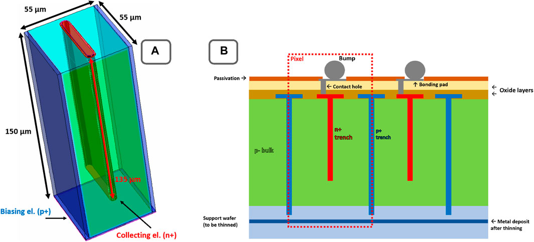
Figure 1. Geometry of a 3D trench-type silicon pixel. (A) TimeSPOT pixel rendering with physical dimensions. (B) Structure of a sensor and its doping profiles (red for n + doping, green for p–doping and blue for p + doping).
The TimeSPOT sensors have been fully characterised in two beam test campaigns featuring both excellent time resolution, of about 10 ps, and detection efficiency of 99% [5, 7–10].
In general, 3D sensors are expected to have an higher radiation hardness with respect to planar silicon sensors due to the shorter inter-electrodes distance which guarantees a lower trapping probability of charge carriers during their motion towards the electrodes [11]. Radiation tolerance of 3D columnar sensors has been already proved up to 3 ⋅ 1016 1 MeV neq cm−2 [12] for what concerns the charge carrier collection efficiency. A similar behaviour is expected also for 3D trench sensors for which however the radiation hardness was never tested. To verify the radiation tolerance of the TimeSPOT sensors an irradiation campaign has been carried out at the TRIGA Mark II Reactor2 at the Jožef Stefan Institute in Ljubljana, Slovenia. Several test structures of the second TimeSPOT batch, produced in 2020 by Fondazione Bruno Kessler (FBK) in Trento, Italy, were irradiated at two different neutron irradiation fluences of 1.0 ⋅ 1016 1 MeV neq cm−2 and 2.5 ⋅ 1016 1 MeV neq cm−2. After irradiation the test structures were stored in a temperature controlled box at about −20 °C, to prevent radiation damage mitigation due to the reverse annealing. Two types of test structures, the single pixel and the triple-strip (Figure 2), were then wire bonded to the readout boards and stored back at −20 °C. In the single pixel structure the innermost of seven adjacent pixels in a row is readout, while the two adjacent pixels are connected to ground, to guarantee the proper electric field configuration. This structure has been used for the charge collection (amplitude) and timing characterizations. The triple-strip structure consists of 30 pixels placed in three adjacent rows which have the readout electrodes shorted together. This device, having a larger active area, has been used for the efficiency measurements.
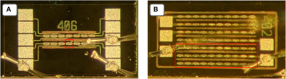
Figure 2. Pictures of some of the 3D pixel test structures used in this work. For each structure the active area is outlined in red. (A) Single pixel sensor; (B) triple strip sensor (30 pixels located in three adjacent rows).
The test structures are readout through the TimeSPOT single channel front-end electronic boards detailed in [13]. This circuit features a signal-to-noise ratio (S/N) of about 20 and an electronic jitter below 7 ps at 2 fC input charge. The power consumption is about 70 mW/channel. The board directly hosts the test structures and provides the bias voltage to the sensors by means of a conductive tape placed on the back side of the test structures (Figure 3).
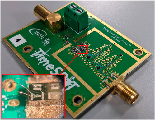
Figure 3. The TimeSPOT single channel board [14]. A magnification of the test structure wire bonded to the board input is also reported.
Irradiated TimeSPOT sensors have been tested in May 2022 at the CERN SPS/H8 beamline with a 180 GeV/c positive hadrons beam. The beam, on average, consists of 106 particles which are extracted every 30 s in a 4 seconds-long spill and focused on an approximately circular spot of 8 mm radius measured at the setup location. The setup (Figure 4) consists of a total of four detectors precisely aligned with respect to the beam line: two 3D trench sensors and two microchannel-plate photo-multipliers (MCP-PMTs). The two 3D trench silicon sensors, along with their respective front-end electronics boards, have been securely installed within an electromagnetically shielded light-tight enclosure.
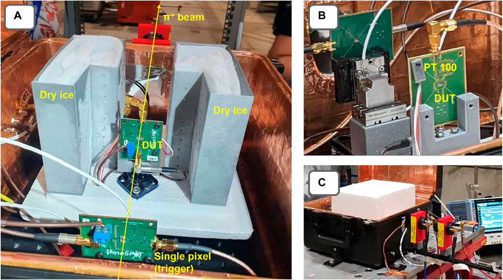
Figure 4. Pictures of the beam test setup. (A) Front view of the light-tight box containing the two silicon sensors aligned; the irradiated sensor is placed between two dry ice containers used for the cooling. (B) Back view of the two silicon sensors in which the temperature sensor (PT100) is visible. (C) Global view of the setup showing the black light-tight box containing the polystirene box, where the irradiated sensor is placed, and the two MCP-PMTs providing the time of arrival of the particles. The oscilloscope used for the signal acquisition is also visible in the picture.
One of the sensors, the irradiated structure, is operated at low temperature. To do that the sensor is placed in a cold, temperature-monitored environment, which is isolated from the other part of the light-tight enclosure by means of a polystyrene box. Dry ice has been regularly filled inside two 3D printed containers positioned inside the polystyrene box. This relatively simple system effectively enables the operation of the irradiated sensors within a temperature range [−40, − 20]°C for about 10 h. The sensor positioned within the polystyrene box is fixed to a stationary mount which only allows to manually rotate the sensor around the vertical direction to measure the sensor response for non-normal beam incidence. The other (non-irradiated) sensor is mounted on a movable holder outside of the thermally isolated box. Such holder is driven by two closed-loop piezoelectric linear stages, allowing movements of up to 16 mm with a position accuracy of 10 nm in the transverse direction relative to the beam line. The second sensor, mounted on the piezoelectric holder, provides a signal for the acquisition trigger allowing unbiased measurements of the device under test (DUT). Two microchannel-plate photo-multipliers are employed for the precise measurement (3–4 ps) of the time of arrival (TOA) of each particle. Both photo-multipliers feature a 18 mm diameter and a 5.5 mm thick quartz input window.
The signals from the silicon sensors and the two MCP-PMTs are processed and recorded by a 8 GHz analog bandwidth 20 GSa/s 4 channels digital oscilloscope. The connection of the sensors and the MCP-PMTs to the oscilloscope is made through low-loss RF cables. The typical trigger requires the coincidence in a time window of 20 ns of two signals, one of the MCP-PMTs and one of the non-irradiated 3D trench sensor, with a minimum amplitude. This trigger condition avoids bias on the DUT measurements, which is not involved in the acquisition requirements. A representative event recorded with the described setup is reported in Figure 5.
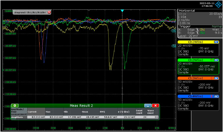
Figure 5. A typical event in which a charged particle crosses the four detectors. The signals from the two silicon sensors are shown in yellow (non-irradiated) and green (irradiated), while the signals of the two MCP-PMTs are reported in orange and blue.
The analysis method strictly follows what discussed in previous publications [5, 8]. Each waveform is processed to determine the signal amplitude and time of arrival (TOA).
A signal is identified by looking for a minimum in the waveform in a time window where signals are expected to contribute. The signal amplitude is determined by subtracting the minimum value found from the corresponding extrapolated value of the baseline, which is determined event-by-event by fitting the first samples of the waveform.
Among the different methods already detailed in [5, 8], the reference and the spline are used in this article. The reference method embodies the amplitude and rise time compensation (ARC) method [15]. In this approach, the signal waveform undergoes a delay of approximately half its rise time, followed by subtracting the delayed waveform from the original. Subsequently, the TOA is determined as the time where the resulting waveform exceeds half of its maximum amplitude. On the other hand, the spline method interpolates the waveforms using cubic splines. The TOA is then set to the time at which the signal exceeds a specified fraction (20%) of its maximum amplitude.
While the reference method has shown the best performance in term of time resolution, the spline method has a wider application being a refined, off-line implementation of the constant fraction discriminator.
The analysis method utilised is proved not to bias the results, which is a fundamental requirement for the measurements that are discussed in the following. In particular, it is capable to reconstruct the observables also in case of very low charge deposits, which is important for the characterisation of the performance of the whole detector under test that typically is not part of the triggering logic.
Radiation generates traps in the silicon bulk that block the charge carriers for a time by far larger than the typical sensor charge collection time. As a consequence, irradiated sensors feature a reduction of both the collected charge and the signal amplitude, which can be mitigated by increasing the bias voltage applied to the sensor. To study this effect, the two 3D trench silicon pixel structures, irradiated at 1.0 ⋅ 1016 and 2.5 ⋅ 1016 1 MeV neq cm−2, are operated at different bias voltages (−20 V, − 40 V, − 100 V, − 120 V and −150 V).
Figure 6 shows the resulting amplitude distributions which are compared to the measurements of the non-irradiated pixel from [8]. Both irradiated sensors feature a clear dependency of the most probable amplitude value on the bias voltage. Notice that since the amplifier boards used for the two irradiated sensors have slightly different gains, an exact quantitative comparison between the most probable amplitude values cannot be done. Nevertheless, it is evident that both irradiated sensors recover a pulse height distribution similar to those of the non-irradiated one when a bias voltage slightly lower than −100 V is applied. Moreover, the fact that the sensor irradiated at 2.5 ⋅ 1016 1 MeV neq cm−2 still shows a regular, Landau-shaped distribution suggests that the radiation hardness limit for such sensors could be even higher.
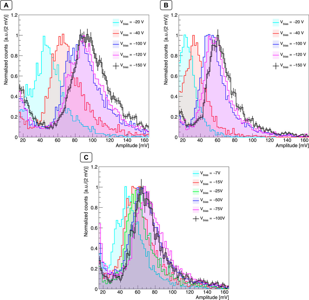
Figure 6. Signal amplitude distributions of 3D trench single pixels for different bias voltage operation at irradiation fluence of (A) 1.0 ⋅ 1016 1 MeV neq, (B) 2.5 ⋅ 1016 1 MeV neq cm−2 and for the (C) non-irradiated sensor.
These measurements clearly prove the radiation hardness of such devices and the unchanged performance with respect to non-irradiated sensors indicate that they can be operated even at fluences higher than 2.5 ⋅ 1016 1 MeV neq cm−2.
The detection efficiency of irradiated sensors is studied in different conditions and compared to the published results of the non-irradiated sensors [8]. The measurement is performed using a triple-strip structure as DUT, and by triggering on tracks crossing a 3D trench single pixel precisely centred, projectively along the beam line, in front of the DUT. A particle detected by the triggering pixel will also cross the triple strip producing a signal unless it ends up inside the trenches or gets trapped in the bulk. The two MCP-PMTs are also readout to obtain a precise charged particle time reference.
The efficiency is given by the ratio η = Nts/Ntr, where Nts is the number of events detected by the triple-strip sensor and Ntr is the number of triggers. Additional requirements on the TOA of the signal in the DUT with respect to the time reference given by the two MCP-PMTs as well as corrections due to small beam divergence are applied following the same methods reported in [8].
Different measurements are performed using the two irradiated 3D trench triple-strip structures: by varying either the bias voltages or the tilt-angle with respect to the beam line. Figure 7A shows the results for the triple-strip structure irradiated at 1.0 ⋅ 1016 1 MeV neq cm−2 as a function of the bias voltage (green points). For Vbias ≤ −60 V the detection efficiency is compatible with the value measured for the non-irradiated sensor (black points). This result is consistent with the recovery of signal amplitude studied in the previous section.
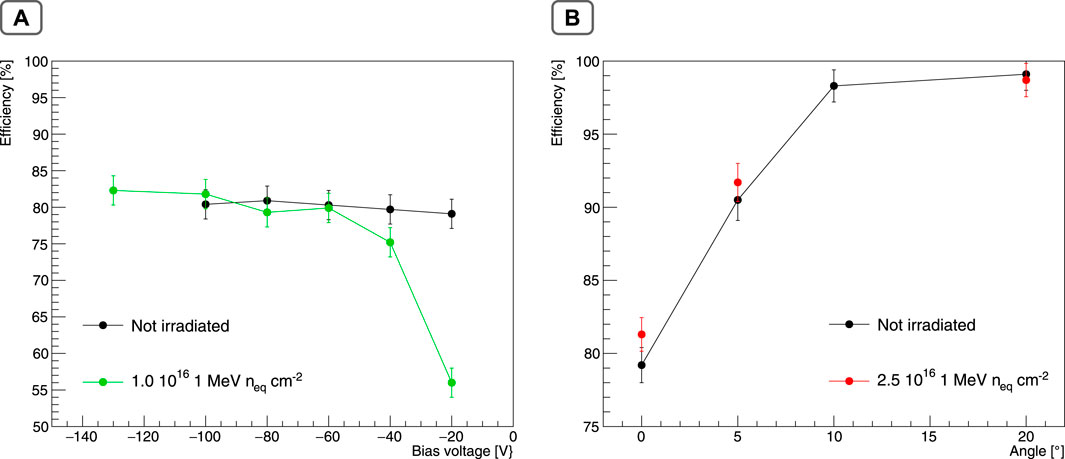
Figure 7. (A) Detection efficiency versus the bias voltage for the irradiated and non-irradiated 3D trench sensors operated at normal beam incidence condition. (B) Detection efficiency versus tilt angle for the irradiated (0°, 5°, 20°) and non-irradiated (0°, 5°, 10°, 20°) 3D trench sensor operated at a bias voltages of −130 V and −100 V, respectively.
Since the trenches are a non-active volume, 3D trench sensors reach the full detection efficiency only if operated tilted with respect to particle flight directions. Therefore, the detection efficiency of the triple-strip structure irradiated at 2.5 ⋅ 1016 1 MeV neq cm−2 is evaluated as a function of the tilt angle and compared to the results obtained for the non-irradiated sensor [8]. The results reported in Figure 7B show that the efficiency of the irradiated sensor (red points) is compatible with that of a non-irradiated sensor (black points) reaching about 99% detection efficiency when tilted at angles larger than 10°. The reported measurements are obtained for a bias voltage of −130 V and −100 V for the irradiated and non-irradiated sensors, respectively.
These results show that the irradiated sensors have the same behaviour of non-irradiated ones by providing higher absolute bias voltage, in agreement to what is observed for the amplitude measurements.
Another key aspect to characterise the detection capabilities of the 3D trench silicon sensor in high radiation environment is given by its timing performance after irradiation.
In this section we report the timing performance of the two 3D trench single pixel structures, irradiated at 1.0 ⋅ 1016 and 2.5 ⋅ 1016 1 MeV neq cm−2, operated at different bias voltages ([−150, − 20]V) at two different tilt angles with respect to the beam line (0° and 20°). For these measurements the acquisition was triggered by the coincidence of signals detected on a non-irradiated silicon strip sensor3 placed upstream the pixel and two MCP-PMTs located downstream. The pixel was carefully aligned in the beam transverse plane with respect to the strip in order to maximise the rate of detected coincidences.
The time of arrival of the tested sensor (tSi) is determined by means of the reference and spline methods discussed in Section 2.3. The timing performance of the sensor are measured with respect to the time reference given by the mean of the two MCP-PMTs TOAs (⟨tMCP-PMTs⟩), which has a precision in the range of 3 ps–4 ps.
Figure 8 shows the distributions of tSi − ⟨tMCP-PMTs⟩ for the two irradiated pixels operating at bias voltage of −150 V. Minimal requirements on the amplitudes of the MCP-PMTs and on the triggering sensor are applied to reject badly reconstructed events. The two distributions are very similar to each other and have the same characteristics as the distribution of non-irradiated pixels (see Figure 9 of Ref; [8]), featuring a narrow peak and a small tail due to late signals. The distribution is fit by the sum of two Gaussian functions describing the signal, and a constant modelling the background. The time resolution of the single pixel,
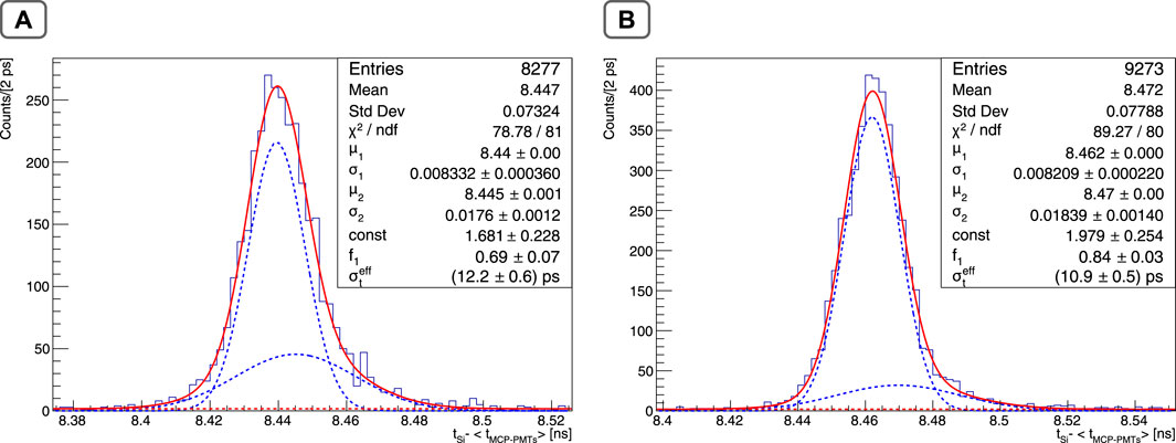
Figure 8. Distributions of the difference between the time of arrival of the 3D trench single pixel (reference method) and the time reference, tSi −⟨tMCP-PMTs⟩ for the single pixel irradiated at (A) 1.0 ⋅ 1016 and (B) 2.5 ⋅ 1016 1 MeV neq cm−2, both operated at Vbias = −150 V. The distributions are fit with the sum of two Gaussian functions (blue dashed lines) describing the signal, and a constant (red dashed line) modelling the background.
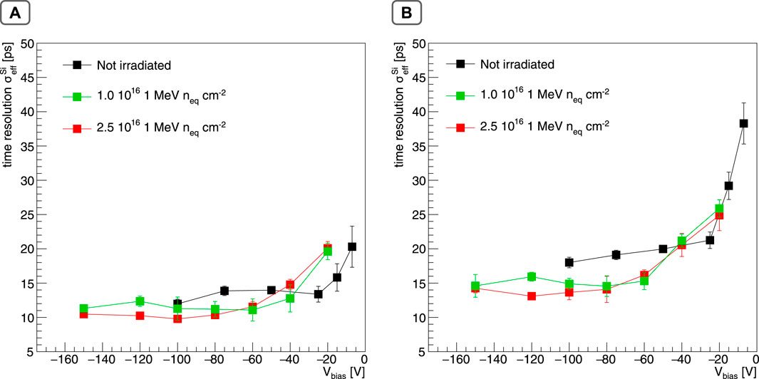
Figure 9. Time resolution of the single pixels as a function of the bias voltage for the different irradiation fluences obtained with the (A) reference and (B) spline methods. The contribution due to the resolution of the time reference is subtracted. Irradiated pixels are operated in a temperature range [−40, − 20]°C, while non-irradiated pixel is operated at room temperature.
Figure 9 shows the resulting values of the time resolution as a function of the sensor bias voltage for the two irradiated pixels and, as a reference, for the non-irradiated one, operated respectively at low (in the range [−40, − 20]°C) and room temperature. Both results obtained with the reference and the spline methods are reported. The irradiated sensors have very similar timing performance to the non-irradiated one. The time resolution obtained with the reference method at a bias voltage of −100 V are 9.8 ± 0.4 ps for the 2.5 ⋅ 1016 1 MeV neq cm−2 pixel and 11.3 ± 0.7 ps for the 1.0 ⋅ 1016 1 MeV neq cm−2 pixel to be compared to the 12.0 ± 0.7 ps of the non-irradiated sensor operated at the same bias voltage. These results clearly show that the time resolution of 3D trench sensor is not affected by the radiation damage up to the considered fluences. The slightly better timing performance of the irradiated sensors with respect to the non-irradiated ones are related to the different performance of the front-end electronic boards used for the different sensors and to the different temperature condition. The measurements also show that the time resolution of both the irradiated and non-irradiated sensors does not improve significantly below a certain value of bias voltage, which is about −25, −60 and −80 V for the non-irradiated, for the 1.0 ⋅ 1016 and 2.5 ⋅ 1016 1 MeV neq cm−2 sensors, respectively. This effect can be explained by the amplitude decrease of the irradiated sensors when operated at lower absolute bias voltages as discussed in Sec. 3.1.
Given the convenience in operating the 3D trench sensors tilted with respect to the particle flight directions in terms of detection efficiency (Sec. 3.2), the time resolution is also evaluated for a tilt angle of 20°. Table 1 show the results for both the non-irradiated and the irradiated (2.5 ⋅ 1016 1 MeV neq cm−2) pixels. Both pixels feature a similar worsening of the time resolution of maximum +40% when operated at 20°. Such behaviour is due to the larger fraction of tracks that crosses adjacent pixels leading to charge sharing between two pixels and thus in a reduced signal amplitude of the pixel under test (see details in [8–10]). As shown in Ref. [8], in such cases the timing performance recovers that of the single pixel at normal incidence by combining the information of the two hit pixels with a clustering algorithm.
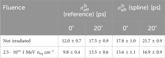
Table 1. Time resolution for non-irradiated and irradiated 3D trench pixels operated at different tilt angles. The contribution due to the resolution of the time reference is subtracted. The sensors were operated at a bias voltage of −100 V.
The innovative 3D trench silicon pixel sensors, developed by the TimeSPOT collaboration, have demonstrated exceptional performance in detecting high-energy charged particles, exhibiting high detection efficiency and precise timing resolution, as highlighted in previous works [5, 8]. This study explores their radiation tolerance, showcasing their resistance up to fluences of 2.5 ⋅ 1016 1 MeV neq/cm2 through measurements conducted during a beam test campaign on irradiated sensors.
Due to radiation damage, the detection efficiency of 3D trench sensor diminishes for Vbias ≥−40 V. However, this reduction is offset by restoring the full efficiency when applying a slightly larger reverse bias voltage. This observation is supported by the analysis of amplitude distributions at various bias voltages, revealing a distinctive peaking shape similar to that of the non-irradiated pixel for bias voltages slightly lower than −100 V.
Crucially, the timing performance of the irradiated sensors match those of their non-irradiated counterparts, underscoring the negligible impact of radiation damage on these sensors.
As of today, 3D trench-type silicon detectors stand out as the fastest radiation-hard charged-particles pixel sensors available. Their promising features position them as a compelling solution for future upgrades in the tracking systems of numerous High Energy Physics experiments that operate at exceptionally high instantaneous luminosity.
The raw data supporting the conclusion of this article will be made available by the authors, without undue reservation.
FB: Formal Analysis, Investigation, Writing–review and editing. AC: Conceptualization, Investigation, Methodology, Writing–review and editing. GMC: Conceptualization, Writing–review and editing. GFDB: Conceptualization, Writing–review and editing. MG: Conceptualization, Formal Analysis, Investigation, Methodology, Writing–review and editing. LLD: Investigation, Methodology, Writing–review and editing. ALai: Conceptualization, Investigation, Writing–review and editing. ALam: Conceptualization, Formal Analysis, Investigation, Methodology, Writing–original draft, Writing–review and editing. ALoi: Conceptualization, Investigation, Writing–review and editing. MMO: Investigation, Formal Analysis, Writing–review and editing. GS: Investigation, Formal Analysis, Writing–review and editing. SV: Investigation, Formal Analysis, Writing–original draft, Writing–review and editing.
The author(s) declare that financial support was received for the research, authorship, and/or publication of this article. This work was supported by the Fifth Scientific Commission (CSN5) of the Italian National Institute for Nuclear Physics (INFN), within the Project TimeSPOT and by the ATTRACT-EU initiative, INSTANT project. This project has received funding from the European Union’s Horizon 2020 Research and Innovation programme under GA no. 101004761.
The authors wish to thank the staff of North Hall Area at CERN for their help in the beam-line setup and operations.
The authors declare that the research was conducted in the absence of any commercial or financial relationships that could be construed as a potential conflict of interest.
The author(s) declared that they were an editorial board member of Frontiers, at the time of submission. This had no impact on the peer review process and the final decision.
All claims expressed in this article are solely those of the authors and do not necessarily represent those of their affiliated organizations, or those of the publisher, the editors and the reviewers. Any product that may be evaluated in this article, or claim that may be made by its manufacturer, is not guaranteed or endorsed by the publisher.
1https://web.infn.it/timespot/index.php
2https://www.tuwien.at/en/trigacenter/trigareactor
3A row of ten 3D trench pixels with the readout electrodes shorted together.
1. LHCb Collaboration. Framework TDR for the LHCb Upgrade II - opportunities in flavour physics, and beyond, in the HL-LHC era. Geneva: CERN (2021). Tech. rep.
2. ATLAS Collaboration. Technical design report for the ATLAS inner tracker pixel detector. Geneva: CERN (2017). Tech. rep. doi:10.17181/CERN.FOZZ.ZP3Q
3. CMS Collaboration. The phase-2 upgrade of the CMS tracker. Geneva: CERN (2017). Tech. rep. doi:10.17181/CERN.QZ28.FLHW
4. Lai A, Anderlini L, Aresti M, Bizzeti A, Cardini A, Dalla Betta GF, et al. First results of the timespot project on developments on fast sensors for future vertex detectors. Nucl Instr Methods Phys Res Section A: Acc Spectrometers, Detectors Associated Equipment (2020) 981:164491. doi:10.1016/j.nima.2020.164491
5. Anderlini L, Aresti M, Bizzeti A, Boscardin M, Cardini A, Dalla Betta GF, et al. Intrinsic time resolution of 3D-trench silicon pixels for charged particle detection. J Instrumentation (2020) 15:P09029. doi:10.1088/1748-0221/15/09/P09029
6. Mendicino R, Forcolin GT, Boscardin M, Ficorella F, Lai A, Loi A, et al. 3d trenched-electrode sensors for charged particle tracking and timing. Nucl Instr Methods Phys Res Section A: Acc Spectrometers, Detectors Associated Equipment (2019) 927:24–30. doi:10.1016/j.nima.2019.02.015
7. Brundu D, Cardini A, Contu A, Cossu GM, Dalla Betta GF, Garau M, et al. Accurate modelling of 3D-trench silicon sensor with enhanced timing performance and comparison with test beam measurements. J Instrumentation (2021) 16:P09028. doi:10.1088/1748-0221/16/09/p09028
8. Borgato F, Brundu D, Cardini A, Cossu GM, Dalla Betta GF, Garau M, et al. Charged-particle timing with 10 ps accuracy using TimeSPOT 3D trench-type silicon pixels. Front Phys (2023) 11:1117575. doi:10.3389/fphy.2023.1117575
9. Garau M. Development of a new silicon pixel detector with 10 ps time resolution for high luminosity future experiments. Italy: University of Cagliari (2023). PhD Thesis.
10. Lampis A. Innovative silicon pixel sensors for a 4D VErtex LOcator detector for the LHCb high luminosity upgrade. Italy: University of Cagliari (2023). PhD Thesis.
11. Da Vià C, Dalla Betta GF, Parker S. Radiation sensors with three-dimensional electrodes. United States: CRC Press (2019). doi:10.1201/9780429055324
12. Lange J, Giannini G, Grinstein S, Manna M, Pellegrini G, Quirion D, et al. Radiation hardness of small-pitch 3D pixel sensors up to a fluence of 3 ⋅ 1016neq/cm2. J Instrumentation (2018) 13:P09009. doi:10.1088/1748-0221/13/09/P09009
13. Cossu GM, Lai A. Front-end electronics for timing with pico-second precision using 3D trench silicon sensors. J Instrumentation (2023) 18:P01039. doi:10.1088/1748-0221/18/01/P01039
14. Lai A, Cossu GM. High-resolution timing electronics for fast pixel sensors (2020). arXiv:2008.09867.
Keywords: particle tracking detectors, solid-state detectors, timing detectors, radiation-hard detectors, radiation hardness, high time resolution, high luminosity
Citation: Borgato F, Cardini A, Cossu GM, Dalla Betta GF, Garau M, La Delfa L, Lai A, Lampis A, Loi A, Obertino MM, Simi G and Vecchi S (2024) Characterisation of highly irradiated 3D trench silicon pixel sensors for 4D tracking with 10 ps timing accuracy. Front. Phys. 12:1393019. doi: 10.3389/fphy.2024.1393019
Received: 28 February 2024; Accepted: 04 April 2024;
Published: 22 April 2024.
Edited by:
Giovanni Paternoster, Bruno Kessler Foundation (FBK), ItalyReviewed by:
Marco Povoli, SINTEF Digital, NorwayCopyright © 2024 Borgato, Cardini, Cossu, Dalla Betta, Garau, La Delfa, Lai, Lampis, Loi, Obertino, Simi and Vecchi. This is an open-access article distributed under the terms of the Creative Commons Attribution License (CC BY). The use, distribution or reproduction in other forums is permitted, provided the original author(s) and the copyright owner(s) are credited and that the original publication in this journal is cited, in accordance with accepted academic practice. No use, distribution or reproduction is permitted which does not comply with these terms.
*Correspondence: A. Lampis, YW5kcmVhLmxhbXBpc0BjYS5pbmZuLml0; S. Vecchi, dmVjY2hpQGZlLmluZm4uaXQ=
Disclaimer: All claims expressed in this article are solely those of the authors and do not necessarily represent those of their affiliated organizations, or those of the publisher, the editors and the reviewers. Any product that may be evaluated in this article or claim that may be made by its manufacturer is not guaranteed or endorsed by the publisher.
Research integrity at Frontiers
Learn more about the work of our research integrity team to safeguard the quality of each article we publish.