 Mohammad Atwany
 Sarah Pardo
 Solomon Serunjogi
 Mahmoud Rasras
- Engineering Division, New York University, Abu Dhabi, United Arab Emirates
Deep learning has revolutionized many sectors of industry and daily life, but as application scale increases, performing training and inference with large models on massive datasets is increasingly unsustainable on existing hardware. Highly parallelized hardware like Graphics Processing Units (GPUs) are now widely used to improve speed over conventional Central Processing Units (CPUs). However, Complementary Metal-oxide Semiconductor (CMOS) devices suffer from fundamental limitations relying on metallic interconnects which impose inherent constraints on bandwidth, latency, and energy efficiency. Indeed, by 2026, the projected global electricity consumption of data centers fueled by CMOS chips is expected to increase by an amount equivalent to the annual usage of an additional European country. Silicon Photonics (SiPh) devices are emerging as a promising energy-efficient CMOS-compatible alternative to electronic deep learning accelerators, using light to compute as well as communicate. In this review, we examine the prospects of photonic computing as an emerging solution for acceleration in deep learning applications. We present an overview of the photonic computing landscape, then focus in detail on SiPh integrated circuit (PIC) accelerators designed for different neural network models and applications deep learning. We categorize different devices based on their use cases and operating principles to assess relative strengths, present open challenges, and identify new directions for further research.
1 Introduction
Since the advent of computers, researchers have been captivated by the prospect of endowing machines with human-like abilities such as abstract thinking, decision-making, creative expression, and social behavior, leading to a field now popularized as Artificial Intelligence (AI). However, the practical use of AI was not realized until theoretical advances in the 1980s and 90s brought a particular form of AI to the forefront: deep neural networks [1]. In the past two decades, deep learning has seamlessly integrated into daily life, from consumer applications like personalized product recommendations, to enhanced medical diagnosis and drug design. This rapid advancement in adoption can be substantially attributed to advances in hardware, both in processing speed and memory capacity [2].
At the same time, the rapid progress in deep learning algorithms and their applications has accelerated the demand for high-performance computing platforms. In 1975, Moore projected a doubling of chip complexity every two years [3], but this trend has since approached a saturation in the possible density for conventional CMOS circuits. Recently, Graphics Processing Units (GPUs) have become the industry standard in scaling computing to meet demands, relying primarily on maximizing the use of parallel processing. AlexNet [4], introduced in 2012, was the first popular convolutional neural network architecture specifically developed for use on general-purpose graphics processing unit (GPGPU) platforms, following earlier proposed implementations such as [5, 6]. Field-programmable gate array (FPGA) accelerators have also been introduced, including the Caffeine platform [7] in 2016, and the Microsoft Project Catapult [8] in 2017. NVIDIA has come to dominate the industry with their A100 accelerator introduced in 2020 [9]. Current benchmarks have shown that a single A100 can train a simple convolutional network to classify images from the CIFAR-10 dataset with 94% accuracy in just 3.29 s [10].
But while these devices have shown great performance in terms of speed and scale, their energy demands are extreme: in 2023 alone, NVIDIA shipped 100,000 units, which will consume an average of 7.3 TWh of electricity annually [11]. Currently, the majority of computational power demands come from data centers and are exacerbated by the increase in popularity of applications like artificial intelligence. Energy demands stem from the electricity supplying power (40%) and cooling requirements (40%), with the remainder attributed to associated compute infrastructure equipment. As a consequence, global electricity consumption by high-performance computing is expected to rise to a total range between 620 and 1,050 TWh by 2026 [11]. This corresponds to an increase between 160-590 TWh: roughly the annual demand of Sweden on the low end, or Germany on the high estimate.
Such trends reflect the fundamental limitations of acceleration through increased chip density and parallelism. As a result, in the search for ways of increasing scale to meet such application demands, research has begun to explore photonic accelerators as novel compute engines [12]. Photonic accelerators, also known as optical accelerators, are built on prior photonic technologies such as modulators, photo-detectors, and optical filters [13] which have been adapted to implement computing operations. This growth in interest is illustrated in Figure 1, with a line plotting publications per year on photonic deep learning accelerators. Unlike traditional electronic components such as transistors and electronic switches, photonic accelerators utilize photons to process information. Photonic devices can make use of the properties of light to enable parallel processing and fast information transfer, with reduced energy consumption and greater efficiency per area.
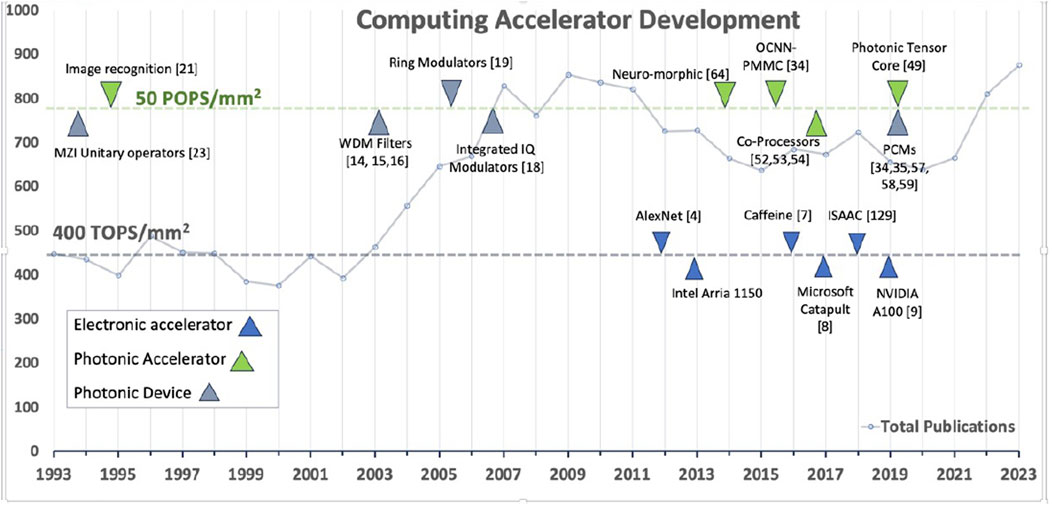
Figure 1. A timeline of milestones in accelerator development. The plot indicates the year in which each technology was introduced, showing the advancements in the 21st century which are foundational for practical photonic accelerators. The trajectory line indicates the number of publications per year on photonic deep learning accelerators in particular. Finally, the two horizontal lines indicate the projected throughput of conventional vs photonic accelerators, measured in tera-ops (TOPs) per area (mm2).
1.1 Computing with light
The development of photonic accelerators has been driven by decades of innovations at the device and chip level of optical systems. These accelerators build upon foundational photonic technologies such as lasers, modulators, photodetectors, and optical filters. Many key developments in optical devices and integrated SiPh circuits have been introduced since the early 1980 s, such as wavelength division multiplexing (WDM) filters [14–16], Mach-Zehnder interferometer (MZI) modulators [17, 18] and in-phase/quadrature (I/Q) modulators [19]. This evolution continued with the advent of smaller-sized Microring Resonators (MRRs), crucial in many optical filter designs, and high-speed or large bandwidth non-return-to-zero (NRZ) modulators [20]. Additionally, Pulse Amplitude Modulation with Four Levels (PAM4) modulation schemes have been explored, using ring resonators to increase the throughput per area of the device [21]. These ring resonators, possessing high-Q factors, have been engineered to function as switches, integrators, differentiators, and memory elements at both optical and terahertz (THz) frequencies.
The earliest optical accelerators could be traced in the assemblage of typical lab bench-top discrete optical components interconnected with long fiber spools intended to perform canonical mathematical functions [22, 23]. One such important task is computing unitary operations, first demonstrated optically by Reck et al. [24] in 1994 using optical beam splitters, Fourier lenses, and light-emitting diode (LED) sources. This development laid the groundwork for subsequent advancements in integrated photonic computations using MZIs. Miller et al. [25–27] showed that such MZI meshes could be self-configured to define a desired function, paving the way for building adaptive systems. Clements et al. [28] improved on the design with an alternative rectangular topology that achieves an equivalent computation using only half the optical depth. These landmark developments are plotted in the timeline of Figure 1.
Optical computing has previously been viewed skeptically in applications that require large data storage and efficient flow control. However, current research demonstrates the capabilities of photonic accelerators on applications that are well-suited to the inherent advantages of optics. These applications include tasks with high parallelism, which can be efficiently computed by non-coherent optics through WDM, polarization diversity, and mode multiplexing [29]. Coherent approaches such as MZI circuits are more challenging to scale, raising concerns about high latency and insertion loss due to the longer physical length of the circuit [30], but MRRs present an alternative with better scalability and compactness. When light goes through ring resonators such as in 2 × 2 switches, the drop port of the switch induces a time delay determined by the Q factor of the ring [31–34]. This induced differential can be used in various ways to transmit information for computations. The latency can be tuned by inserting phase change materials (PCMs) as cladding, or cascading additional switches in tandem. The phase transition of the PCMs leads to appreciable alterations in their optical properties, controllable either electrically or optically [35, 36]. This characteristic offers a notable advantage in power efficiency for programmable photonic devices, compared to electro-optic or thermo-optic methods [37, 38].
Moreover, incorporating non-volatile PCMs as photonic devices enables optical memory storage and in-memory computing, achieved by transmitting optical input through the programmed device. For instance, optical memory in ring resonators has been studied using the Volterra series in microwave photonics [39]. The memory effect is modeled as a multidimensional impulse response in the time domain or Volterra kernels in the frequency domain. By using the ring resonator as a differentiator, it is possible to induce nonlinear mixing of multiple wavelengths to realize a frequency-dependent memory function.
More recently, these devices have been integrated to create energy-efficient, compact, and high-throughput computational accelerators. A comparative analysis of the theoretical maximum tera-operations per second per square millimeter (TOPs/mm2) for both electronic and photonic accelerators shows a clear advantage in the photonic domain.
To calculate the theoretical maximum TOPs/mm2 for electronic accelerators, we consider the operational frequency (F), transistor density (D), and operations per cycle per transistor (O). The formula used is:
For NVIDIA A100 [43], based on the TSMC 7 nm node [44], the parameters are approximately: F = 2 GHz = 2 × 10⁹ Hz, D = 108 transistors/mm2, and O = 2, which gives an estimate of 400 TOPs/mm2. However, due to constraints in practice, in the literature many electronic devices report a maximum efficiency of approximately 100 TOPs/mm2 [46, 47].
In contrast, for photonic accelerators, key parameters include the parallelism factor (P), component integration density (C), and efficiency factor (E). Their relationship is:
Taking the accelerator of Liu et al. as a conservative benchmark [45], representative current parameters are p = 16384, C = 104 components/mm2, and E = 1, giving an estimate of 32 TOPs/mm2.
But while physical limitations increasingly constrain further enhancements in transistor density and operations per cycle for electronic accelerators advances in photonic technology may enable p = 50,000, C = 105 components/mm2, and E = 1, potentially leading to 5000 TOPs/mm2, or 50 POPs/mm2—performance measurable in peta operations per second.
Developments in photonic accelerators, alongside those in conventional hardware accelerators, are depicted in Figure 1, which contrasts these comparative projected throughput capabilities of photonic computing versus electronic computing in terms of TOPs (tera-operations) per second normalized by processor area.
The significantly higher level of projected TOPS/mm2 for photonic systems is attributed to the efficient parallelism achieved through utilizing multiple wavelengths, coupled with a smaller footprint per wavelength.
In silicon nitride (SiN) photonics-based devices, the area of one MAC unit cell is 285 × 354 μm2 [48, 49]. This, when operating at 12 GHz with 4 input vectors via WDM, corresponds to a compute density of 1.2 TOPS/mm2. If silicon-on-insulator (SOI) MRR devices are used instead with a nominal bend radius of 5μm, the area of the MAC unit cell could be reduced to less than 30 × 30 μm2, increasing the compute density to 420 TOPS/mm2 per input channel [50, 51]. In-memory-computing photonic tensor cores show predicted compute density and compute efficiencies of 880 TOPS/mm2 and 5.1 TOPS/W for a 64 × 64 crossbar core at 25 GHz clock speed [52]. Compared with digital electronic accelerators (ASIC and GPU), the photonic core has 1 to 3 orders of magnitude improvement in both compute density and efficiency. Overall, this comparison underscores the advancements and potential of photonic technologies in achieving higher throughput and efficiency in computing. This makes it a competitive candidate for application in the context of neural network processing and deep learning acceleration.
1.2 Photonics for deep learning
Researchers have been interested in optical implementations of neural networks since the 1980s [40], for instance, exploring image recognition by the use of nonlinear joint transform correlators [22], and implementing Hopfield neural networks [41, 42]. Since then, many innovations have stemmed from advancements in photonic tensor cores, in-memory computing, and hybrid co-processors [35, 53–57]. For instance, in deep learning inference, trained weights may not require frequent updates or any at all, making non-volatile analog memory advantageous. This can be achieved using PCMs, either optically [58, 59] or electronically [60, 61]. On the other hand, a real-time neural network can be established by using digital electronic drivers with photonic-compatible firmware. Neuron behavior can be replicated through a hybrid of well-modeled electronic nonlinearities and optical systems that have negligibly low losses. In those systems, the active components consist of photodetectors (PDs) and modulators that inject or deplete carriers in response to an induced electric field [62, 63].
Photonic computing and its use in artificial intelligence applications can be viewed from a multitude of perspectives, many of which have been previously explored in reviews. Various reviews have been devoted to photonic analog computing broadly, such as Stroev and Berloff [64]. Huang et al. [65] provide a survey of design factors in neuromorphic computing, and discuss the role of photonic processing for implementing aspects such as interconnects, linear vs nonlinear operations, and memory, as well as presenting use cases in communications, nonlinear programming, and cryptography. Wu et al. [66] review analog optical computing based on integrated photonics, diffractive networks, and hybrid optoelectronic designs applied specifically to three classes of machine learning models: feed-forward networks, spiking neural networks, and reservoir computing.
In this review, we present a concise overview of the photonic accelerator landscape to provide context for photonic deep learning accelerators (PDLAs), and provide some background on elements of the compute operations in deep neural network architectures that are mapped onto photonic implementations. We focus on Silicon Photonics Integrated Circuit (Si PIC) accelerators, as this modality can be considered more practical for near-term use given its level of technical advancement, cost-effectiveness, and compatibility with conventional CMOS hardware. Our analysis seeks to unify low-level design considerations in implementing PDLAs with a broader perspective on application. The paper is organized as follows: in Section 2, we give context on the broader area of photonic accelerator design: physical modalities, as well as analog and digital compute paradigms. Section 3 provides an overview of the computational building blocks in deep learning, and indicates the roles that photonic accelerators can play in neural network models. In Section 4, we highlight specific approaches to PDLA design with representative examples from the literature. Finally, Section 5 indicates ongoing challenges in implementing PIC-based systems and promising further directions for research, with key takeaways for both photonics and deep learning practitioners.
2 Photonic accelerators
Photonic principles can be used for accelerated computing in many ways, so we first provide context on the primary physical modalities used in a photonics processor. Those devices can also operate in both analog and digital computing paradigms, and we provide examples of each approach. Figure 2 shows this schema of physical and computational properties of photonic accelerators.
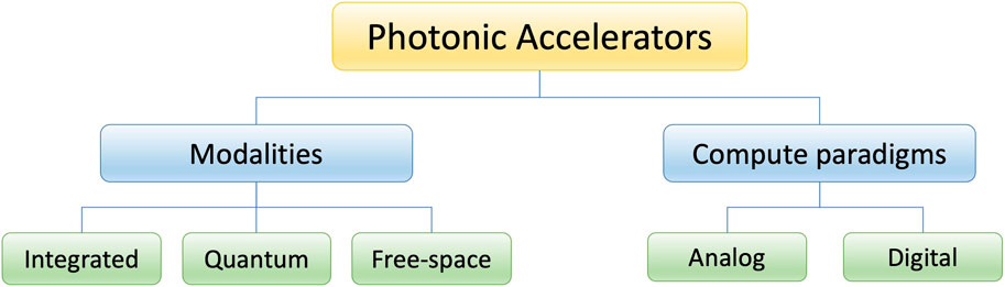
Figure 2. Schema of structural and computational factors in photonic accelerator design.
2.1 Physical modalities
Optical Processing Units (OPUs) are photonic devices used for computing tasks, efficiently performing a broad range of mathematical and logical tasks crucial for applications such as deep learning. These devices leverage optics instead of electronics, in contrast with traditional CMOS processors such as CPUs, GPUs, and TPUs. OPUs have demonstrated scalability in facilitating acceleration within standard computing frameworks [67]. High-bandwidth optical interconnects are central to optical data transmission accelerators, and recent advances here have focused on increasing data rates, decreasing power consumption, and achieving higher reliability [52, 68]. OPUs can be based on three main modalities: integrated optics, quantum optics, and free space optics.
2.1.1 Integrated circuit OPUs
Photonics Integrated Circuits (PICs), the predominant form of OPUs, are engineered for efficiency in operations such as matrix multiplication and convolution [69]. Integrated optical processors have been demonstrated for implementing matrix-vector multiplications at Gb/s processing rates [70–72]. Companies like Lightmatter1, Lightelligence2, Luminous3 are developing photonics ICs for low-power multiply-and-accumulate (MAC) computations which significantly outperform conventional digital and analog electronics.
Adaptive and reconfigurable OPUs also represent an emerging subgroup with the ability to dynamically alter processing parameters, an essential requirement for many machine learning use cases [75]. Programmable OPUs eliminate the need for physical hardware modifications, ensuring cost-effectiveness and resource efficiency. Harris et al. [76] reviewed progress made in Programmable Nanophotonic Processors (PNPs), which employ both classical and quantum information processing. Bogaerts et al. [77] present a survey of the photonic building blocks, as well as discussing the necessary control structures and application-level considerations, for instance highlighting the need for developing descriptive languages similarly to FPGA programming.
An important approach in reprogrammable device design is the use of phase-change materials (PCMs). For example, Wu et al. [35] propose a compact, programmable waveguide mode converter based on a Ge2Sb2Te5 (GST-enhanced) phase-gradient metasurface. The converter uses changes in the refractive index of GST to control the waveguide spatial modes up to 64 levels. This contrast represents the matrix elements, with a 6-bit resolution to perform matrix-vector multiplication in convolutional neural networks. The design featured high programming resolution and was used to construct a photonic kernel using an array of such phase-change metasurface mode converter (PMMC) devices, enabling an optical convolutional neural network to be designed for image processing and recognition tasks. The authors use nanogap-enhanced potential for a wide range of optical functions, making them suitable for large-scale optical computing and neuromorphic photonics.
Innovations in this category also address the issue of noise through advanced noise reduction and error correction techniques, which are important properties in supporting the accuracy and reliability of machine learning computations [78]. The researchers in [79–82] offer a comprehensive review of PCMs in non-volatile photonic applications. They highlight the retention of the optical state of a material without the need for continuous power supply, and the potential for low-energy operation due to the efficient transformation between amorphous and crystalline states, providing a pathway to highly reconfigurable photonic devices.
2.1.2 Quantum OPUs
Quantum OPUs represent another approach to OPU design. These devices have been previously developed and applied in the context of communications [83, 84]. Quantum OPUs can implement compute tasks on very small scales. For example, quantum dots are devices that have small dimensions of a few nanometers. Quantum Dot (QD)–based OPUs incorporate quantum dots, nanoscale semiconductor particles with dimensions of several nanometers, to enhance OPU functionality. Semiconductor QDs represent a type of zero-dimensional, quantum-confined device which exhibits distinct electronic and optical characteristics. The three-dimensional quantum confinement within QDs leads to the total localization of carriers, producing a discrete spectrum characterized by a δ-function-like density of states [85]. The precision control afforded by these quantum dots over photon emission and absorption translates to more effective processing tailored for specific machine learning tasks, thereby expanding the versatility of photonic processing applications [86].
Lingnau et al. [87] furthered the domain with the use of coupled quantum well devices on-chip, highlighting their potential in creating excitable neuromorphic networks [88]. Present a PIC consisting of quasi-single-mode slotted Fabry–Pérot lasers coupled via an actively pumped waveguide. This research shows how quantum optics can enable a variety of controllable excitable states, including dual-state excitability and dual-state bursting mixed-mode oscillations. A state-of-the-art large-scale integrated quantum photonic circuit [89] has been successfully demonstrated in silicon, boasting 16 waveguide spirals, 93 reconfigurable thermo-optical phase shifters, 122 MMIs, 64 grating couplers, and 376 crossings. This reconfigurable device showcased its capabilities in generating, manipulating, and managing (GMM) entangled states directly on the chip.
Quantum photonics can allow for implementing quantum algorithms on an integrated device, for instance implementing Shor’s algorithm to factorize 15 into 3 and 5 [90]. This system comprises a Quantum Fourier Transform subsystem and a two-qubit controlled NOT gate. Variants of quantum photonic algorithms akin to these have been employed in solving a standard eigenvalue problem [91], as well as in the implementation of graph-theoretic algorithms utilizing a SiPh quantum walk processor [92]. However, realizing these quantum-enhanced accelerators presents many technical challenges and feasibility questions [93]. Processing single photons in large quantities requires high-speed, low-loss optical switches like lithium niobate and barium titanate. Achieving the complete integration of quantum circuits, including sources and detectors, remains an unresolved endeavor.
2.1.3 Free-space photonics
Free-space optics represents a pivotal modality in optical computing, diverging from traditional silicon-based mediums to leverage plane light propagation in free space. This approach, as Hsu et al. [94] highlights, exploits additional degrees of freedom such as polarization, diffraction, and orbital angular momentum (OAM), making it particularly suited to tasks involving imaging data and computer vision applications. The use of diffraction for manipulating incident light, as demonstrated by Zhu et al. [95], and the implementation of a Laguerre-Gaussian mode sorter (LGms) for super-multimode (de)multiplexing in optical communications by Fontaine et al. [96], underscore the versatility and potential of free-space optics in enhancing optical computing capabilities.
Deep diffractive neural networks (D2NNs) stand as a notable application of free-space optics. Lin et al.’s D2NN uses passive diffractive layers to implement transforms, though it lacks rapid programmability [97]. Another D2NN design employed orbital angular momentum (OAM) to adjust the phase and amplitude across multiple diffractive screens, enabling the manipulation of light beams’ wavefronts for a trainable network architecture. Hamerly et al. advanced the application of free-space optics in optical computing by employing quantum photoelectric multiplication to implement matrix-vector products through coherent detection [98]. This method not only allows the optical encoding of weights and inputs but also supports the reprogramming and training of the accelerator. Capable of operating at GHz speeds with sub-attojoule energy per MAC, this accelerator scales to larger networks with N ≥ 106 neurons. Another demonstration of D2NNs is reported in [99, 100] with programmable optoelectronic devices as well as additional variants such as D-NIN-1, and D-RNN. Such capabilities indicate the increasing potential of free-space devices in realizing practical, large-scale applications in areas like deep learning, marking a departure from fully integrated photonic processors.
Free-space devices show promise for large scalability, as shown by the LightOn OPU [73] which can operate at 50 TOPS/watt with input vector dimensions of 1 million × 2 million. This OPU can accelerate randomized numerical linear algebra algorithms by implementing very large random matrices optically. It shows how optical properties such as scattering can circumvent the limitations of a von Neumann architecture by performing high-dimensional operations in a single computational step, reducing the effective complexity from O(n2) to O(1). Moreover, the exploration of complex analog computations in free space, as investigated by Cordaro et al., further exemplifies the innovative uses of this technology [101]. Their work on using a silicon metasurface-based platform to solve Fredholm integral equations of the second kind illustrates the broad applicability and the advanced computational possibilities enabled by free-space optics. Collectively, these developments not only underscore the technological advancements in free-space optical computing, but also highlight its expanding role in addressing sophisticated computational challenges.
2.2 Computing paradigms
Analog processors leverage the continuous-time and space properties of light to perform computations, whereas digital photonic accelerators use digital encoding. This flexibility offers two approaches to processing photonic signals and to designing photonic accelerators for machine learning tasks.
2.2.1 Analog optical processing
Analog Optical Processing Units (A-OPUs) [64] use the continuous values generated by the physical functionality of the device by reading them out as computation results, to perform operations like weighted summation in an energy-efficient manner. This is particularly useful in scientific simulations and optimization problems, where continuous solutions are desired. Figure 3 shows an example of an A-OPU suited to solve partial differential equations (PDEs) and ordinary differential equations (ODEs) [102]. When the temporal frequency of the input signal is near the resonant frequency of the phase-shifted Distributed Feedback Semiconductor Optical Amplifier (DFB-SOA), the resultant transfer function becomes equal to that of a first-order linear ODE. Adjusting the injection current at the input tunes the constant coefficient of this ODE. In this way the phase-shifted DFB-SOA can be used to implement a photonic ODE solver by controlling the injection current.

Figure 3. Schematic of an analog photonic ODE solver. (A) When injection current
Analog photonic processing has also been applied to reservoir computing (RC). Originating from concepts in liquid-state machines and echo-state networks, RC is a type of machine learning framework which maps inputs into a fixed non-linear system, known as a “reservoir,” then processes this information through a trainable readout mechanism to produce the model output [103]. The reservoir can be implemented in many ways, and A-OPU devices are increasingly explored as analog reservoirs, showing success when applied to time-series data processing and pattern recognition tasks [104–107]. Further, A-OPUs have also played a role in quantum photonic processing, as seen in Continuous-variable Quantum Optical Processors (CQOPs) [84, 108–111]. The analog approach uses the inherent properties of photon behavior to efficiently perform quantum simulations or produce solutions to optimization problems [64].
2.2.2 Digital optical processing
Digital Optical Processing Units (D-OPUs), on the other hand, use discrete photonic signals for computation and processing [112, 113]. D-OPUs are often designed around enabling typical computing operations like binary logic and bit manipulation, but in a fast and efficient manner using the optical domain. Gostimirovic et al. [114] proposed a hybrid photonic-electronic circuitry for a digital logic architecture using ultra-compact vertical pn junctions based on microdisk switches. With higher Δλ/V, where V is the voltage, they used wavelength-division multiplexing to implement NAND, NOR, and XNOR operations with a single MRR switch. The gates are then expanded to explore complex CMOS-compatible blocks such as adders, encoders, and decoders. Several aspects of optical logic computing have also been explored using semiconductor optical amplifiers (SOAs) [115, 116]. Many mathematical operations can be implemented using Binary Photonic Arithmetic (BPA) where photonic accelerators perform binary arithmetic operations using discrete optical signals [117]. Digital photonic data transmission has also emerged in optical interconnects for data compression, multiplexing, and encoding. These technologies facilitate digital data handling between processing units and memory components in high-performance computing clusters.
In addition to standard bit operations, quantum photonic devices can be used to achieve qubit behavior to facilitate quantum algorithms. Such Quantum Digital Optical Processors (QDOP) [118] can reach ultrafast (1 Tb/s) speeds for optical logic operations [119]. In this context, quantum dot (QD) SOAs have advantages such as minimal crosstalk between adjacent wavelength channels due to QD isolation, which suppressed carrier transfer between dots, and utilization of the cross gain modulation (XGM) effect between two wavelength channels [120, 121]. These QDOP units would enable quantum computations and algorithms that work with digital quantum information, facilitating quantum-enhanced machine learning algorithms.
3 Photonic deep learning fundamentals
Photonic accelerators for deep learning are built on the functionalities of photonic devices highlighted in Section 2. The fundamental goal is to perform the intensive computations required by deep neural networks efficiently and at high speed. Neural networks are built out of linear products and nonlinear special functions. Deep networks include many layers of these operations, which results in their computational expense. Accelerator design can target different components of a network, from the lowest level of mathematical operations to higher-level architecture blocks. Here, we present an overview of the main neural network components and the ways that they are translated to photonic implementations, along with some ways in which performance considerations must be reinterpreted.
3.1 MAC operations in neural networks
The bulk of a network’s computation comes from the matrix multiplications present in layer transforms, and one way to assess network complexity is to count the number of multiply-accumulate (MAC) operations required to evaluate the full network on a given input. For a modified state a′ and a given accumulation variable a, a MAC operation can be written as
In the general case of a linear layer in a network, the action of the layer on an input consists of a weighted sum
“Neurons” xi from layer i transfer signals to neuron xj in the following layer j through connection weights wij, linking a set of input and output variables. bj is a “bias” offset for translation, making it an affine transform. f{⋅} represents a discriminatory nonlinear “activation” function [122, 123]. In a typical network, this is chosen to be either a sigmoid-shaped function, such as the logistic or hyperbolic tangent functions, or a ramp-shaped function, such as the rectified linear unit (ReLU = max{0, x}). The output variables xj are often referred to as the “activations.” The weighted sum of Eq. 1 forms a set of parallel MAC operations and is thus computed as a matrix multiplication of size N × M to convert an input of size M to an output of size N, and in terms of computational complexity often accounted for as
Convolutional neural networks, on the other hand, act on windows of the input tensor, making use of the locality of information in data. As a result, they are especially suitable for tasks on images and other natural signals. Conceptually, a 2D convolution layer takes in a 3D input tensor of size (H × W × Cin) and a 4D kernel tensor of size (Cin × Cout × k0 × k1), and outputs a 3D tensor of size (H × W × Cout). Overall, the layer must apply the kernel transform to all k0 × k1 windows of the input, multiplying them together and summing the values in a convolution operation. In practice, kernel windows are usually square and relatively small (width
Computationally, there are many ways of formulating this multiple-channel, multiple-kernel convolution as generalized matrix-matrix multiplication (GEMM) suitable for modern hardware [125]. The im2col algorithm is often used as a conceptual basis, vectorizing the input such that its values are duplicated for multiplication with the kernel. This naive construction results in a matrix multiplication between matrices of size M × (ck2) and (HW) × (ck2), as depicted in Figure 4 [126]. Here the desired number of output channels is reflected in the value M. Modern GPU implementations derive their efficiency from optimizations such as re-using intermediate results and reducing the amount of matrix reshaping. They also apply virtual memory strategies so that re-used values are never physically duplicated in memory.
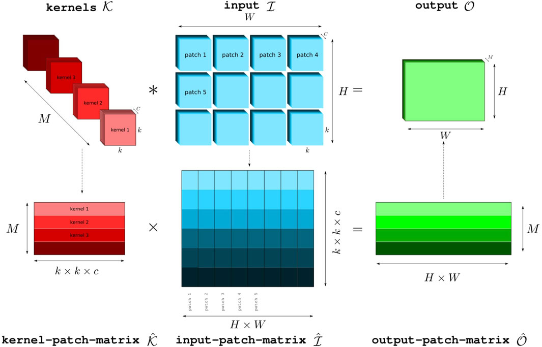
Figure 4. A depiction of the basic im2col formulation of multi-channel multi-kernel convolution as a generalized matrix-matrix multiplication (GEMM). Reproduced from [105], © IEEE.
3.2 Photonic network principles
Designing PIC accelerators for deep learning relies on translating photonic capabilities to these essential building blocks of neural networks. Accelerators can target the linear operations of feedforward and convolution layers through fast photonic multiply and accumulate methods. They can also target nonlinear functions through switching and modulating.
As an illustration, in their groundbreaking work, Shen et al. [127] laid out a construction of how photonic elements can be mapped onto the components of a feedforward neural network for an all-optical procedure. The linear operation of matrix multiplication can be formulated as a unitary operation and readily implemented in programmable photonic circuits (PPC), where phase shifters can tune the optical paths, allowing reconfiguration of neural network weights. Nonlinear activations can then be performed using optical switching elements such as saturable absorbers. They also observe how in-situ training of such an accelerator can be realized photonically not by the backpropagation algorithm standard to digital NNs, but rather by forward propagation and finite differencing to directly obtain the gradient of each parameter. Following the PPC approach of Shen et al., many accelerators choose to implement linear operations photonically using PPC for universal unitary operations. More recently, as an alternative to general MZI mesh designs, Shokraneh et al. [128] designed a “diamond” mesh structure specifically optimized for use in neural networks.
In contrast with coherent, PPC-based designs, the other main concept for linear operations in photonic accelerators is to leverage non-coherent photonics through wavelength division multiplexing (WDM) for parallel operations at scale. The broadcast-and-weight protocol of Tait et al. [129] applied the analogy of the broadcast-and-select WDM protocol by observing the similar network connectivity of neurons between layers. Tunable filter banks based on microring resonators (MRRs) can thus be used similarly to how wavelength demultiplexers are realized in conventional digital interconnects. While the protocol was originally introduced for linear network layers, conceptually this extends naturally to convolutional layers, as a linear layer is equivalent to a convolutional layer with a “1 × 1” kernel. Feldmann et al. [130] have since demonstrated a photonic tensor core that combines the abilities of microcombs and phase-change materials to realize efficient encoding of data and kernels, respectively. Movement of data is minimized with in-memory photonic MAC operations and reduces footprint cost by multiplexing within a single core. Meanwhile, Xu et al. [131] introduced a convolutional accelerator that emphasizes maximized input size capacity, handling full-resolution images of 500 × 500 pixels by making use of both time and wavelength interleaving.
Photonic devices are naturally suited to the linear nature of matrix multiplication, but it is also possible to implement all-optical activations with optical switching implemented for instance in the action of a saturable absorber or nanocavities, as suggested by [127]. Other possibilities include using carrier effect in MRR, or state changes in a material as in a structural phase transition [65]. In addition, some accelerators implement pooling operations photonically, for instance with ring modulators [132], or MMIs [133]. However, the power consumption required to trigger activation switches and to maintain a sufficient signal-to-noise ratio at receiving photodetectors can dominate otherwise passive multiplication steps [127]. As such, many accelerator designs compute these functions in a hybrid optoelectronic manner, converting the output to the electronic domain between multiplication layers.
In addition to handling the arithmetic intensity of deep learning applications, memory implementation is an essential consideration when developing practical hardware accelerators. One important implementation is memristors. Memristors, or resistance switches, were first proposed theoretically as the completion of the three other “fundamental” electrical components: resistors, capacitors, and inductors [134]. The internal state of a memristor is a function of the history of current and/or voltage which has passed through it [135]. Devices that contain “crossbar” arrays of connected memristors have been successfully applied in deep learning applications. A noteworthy example is the ISAAC accelerator [136], which introduced the use of electronic memristive crossbar arrays. Since then, optical memristors have shown improved efficiency over electronic versions in accelerators. Mao et al. [137] provide a comprehensive overview of how practical memristor behavior can be implemented with photonic elements, and highlights how memristors can have various functionalities for light detection, data storage, and in-memory computing. Choi et al. [138] demonstrate a model of in-memory processing that can be realized by photonics integrated circuits using coupled resonators, where the coupled memristive quantities are the intensity distribution and optical coherence. They indicate that their design is scalable to neural network applications.
3.3 Performance considerations
When translating neural network computation to alternative hardware, it can be challenging to make direct comparisons in different aspects of performance. In conventional hardware, the layer transform is considered the primary MAC hardware bottleneck as layer size grows [139]. Figure 5 indicates the requirements in hardware which performs MACs individually and does not compute in memory. In this case, network MACs can be counted uniformly, and for modern networks such as Vision Transformer or ResNet, this can reach 500 billion MACs in a single forward pass4. However, a full optical matrix multiplication can be performed, in principle, in a single step, without consuming any power, independent of the matrix size [127, 140]. The main sources of energy consumption or latency are generally shifted to aspects of transmission, modulation, and detection, performed by various components in the device [139], so photonic device architectures must make tradeoffs in balancing these factors.
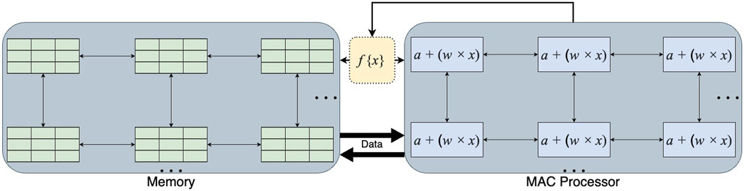
Figure 5. An illustration of the signal pathway required for MAC in a modern chip. The passing of information occurs between MAC processors performing a + (w × x), memory caches, and non-linear operations f{⋅}. Reproduced with permission, from [139], Nahmias et al. 2020 © IEEE.
As a result, the complexity of photonic MAC operations must be conceptualized differently than in conventional hardware. In the photonic case, “complexity” is no longer tied to algorithmic complexity in terms of counting individual multiply-accumulate steps. As Miscuglio et al. state, “one must distinguish between the complexities of the computational algorithm vs that of the system’s execution time” [140]. By comparison, it is important to note that GPUs are still bound by the O(N2.8) (Strassen [141]) or O(N2.373) (Coppersmith-Winograd [142]) complexity of matrix multiplication algorithms, and their optimization is in reduced system execution time due to parallelism, value re-use, and minimized I/O cost. In order to make comparisons, a more appropriate frame is to think of “effective” MACs per time. For instance, when we say that a photonic operation is “O(1),” we mean that the entire computation is executed in a single “atomic” computing operation. In a passive component, this can effectively be the speed of light propagating through the medium. This is also why compute density becomes a more important metric to consider, as photonic components may individually be larger, but a single component can implement many “effective” MACs. As a result, many accelerators report normalized performance statistics in terms of operations per area.
Another distinction arises particularly in analog photonic accelerators in the way that “bit precision” is translated to photonic hardware. As discussed by Shiflett et al. [143], “While we use the terminology ‘bits of precision’ for analog photonic computation, what we are actually describing is the log2 of the number of separable optical power amplitudes at the output.” Numerical precision becomes reliant on the signal-to-noise ratio of transmission among device components. This presents a source of energy overhead as for instance the power of input lasers must be increased in order to increase this ratio. In the case of MRR-based designs, a tradeoff between multiplexing parallelism and numerical precision may also arise, through the power cross-coupling coefficient k2: roughly speaking, lowering it reduces crosstalk, but also increases losses. Changing the spacing of MRRs will have an impact on the overall footprint of the device. The number of components for parallelism in turn impacts the amount of added time that may be incurred if operations must be performed sequentially, in case the data size exceeds the capacity of a single optical element. One way to normalize for these effects is to assess the efficiency of the WDM usage in terms of energy per wavelength utilized [143].
In practice, it can sometimes be more efficient to use hybrid methods that offload some network tasks to standard electronic implementations, in which case energy consumption and speed limitations are incurred in optoelectronic conversion. The added energy expense can come from the receiver stages that follow detection, which may consist of amplification, sampling, and quantization [129]. Many accelerators apply nonlinear layers in the electronic domain, and some even combine photonic multiplication with electrical addition [144, 145], especially when network weights or activations are reduced to one-bit representations. Optoelectronic conversions can introduce speed bottlenecks not only through DAC/ADC conversion steps but also by reverting to a dependence on electronic clock rate for sequential operations.
4 Integrated photonic deep learning accelerators
In this section, we discuss examples of integrated circuit PDLAs which explore the challenge of mapping deep learning onto photonic hardware, showing comparative advantages and tradeoffs in various approaches. We group the accelerators on an application level according to important deep learning use cases: convolutional networks; linear models and sequence processing; and real-time or edge computing applications. These examples implement popular existing neural network architectures, which can facilitate nearer-term adoption. We provide two tables to aggregate main operating principles (Table 1), and summarize features and figures-of-merit (Table 2). Figure 6 shows the high-level application categories.
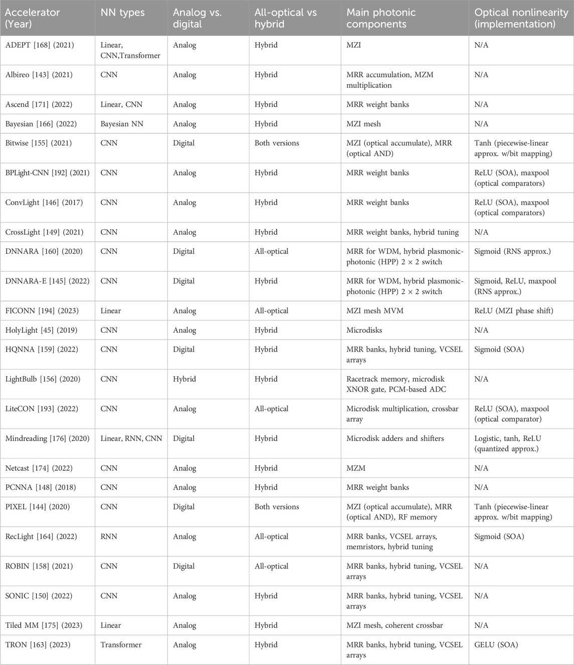
Table 1. High-level properties of the accelerators featured in the review.
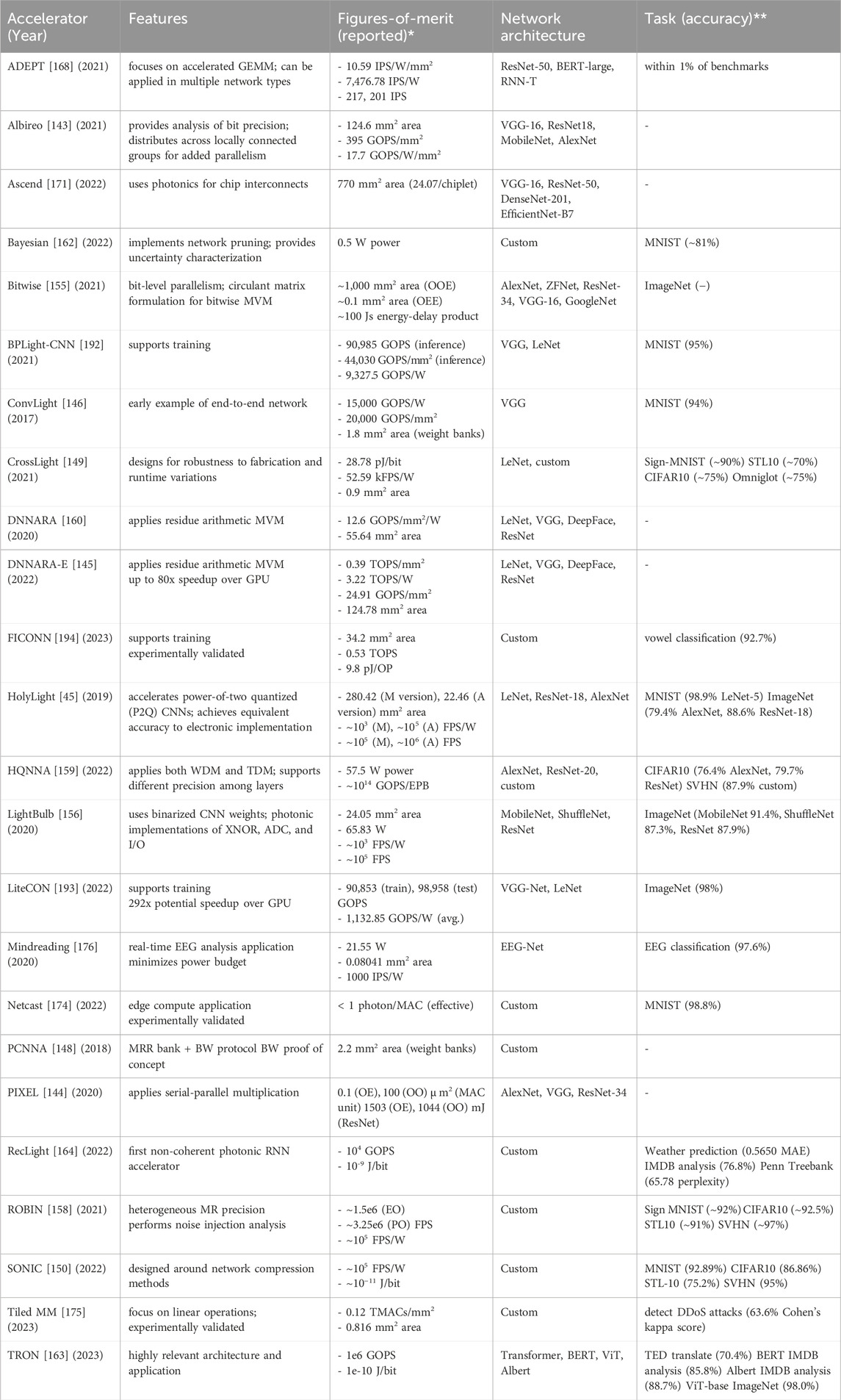
Table 2. Features, figures-of-merit, and applications of accelerators. We reproduce metrics in the form reported by the paper, as not all accelerators report consistent figures-of-merit. Approximate values are indicated by “∼” where only relativevalues were reported, or were only reported visually in a plot. “—” indicates that a value was not directly reported in the paper. Acronyms: GOPS = giga operations/second; IPS = inferences/second; FPS = frames/second; MVM = matrix-vector multiplication; EPB = energy per bit.
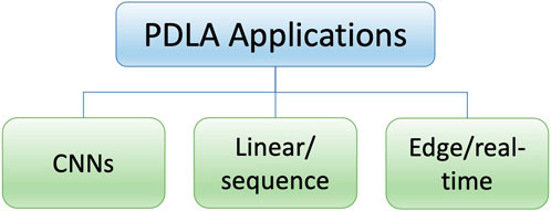
Figure 6. Areas of application which can be accelerated by PDLAs.
4.1 Focus on CNNs
A prominent approach in photonic accelerators for deep learning is focused on implementing convolutional neural networks (CNNs) for fast photonic inference on computer vision tasks. Many convolution accelerators are based on WDM and resistive memory, which are implemented through configurations of components such as ring resonators, modulators, and interferometers. The WDM parallelism can be applied in an analog manner, or in a digital manner acting on different bits in parallel.
An early entry into photonic CNN accelerators was ConvLight, introduced by Dang et al. [146]. ConvLight implements an end-to-end architecture, with feature extraction blocks applying memristive convolution, semiconductor-optical-amplifier (SOA) ReLU activation, cascaded optical comparators for max pooling, and finally a memristive linear layer. The convolution unit comprises a WDM waveguide, a Weight Resistor Array (WRA) based on memristors, a Ring Modulator Array (RMA), and an SRAM buffer (SB). Weight values are stored in memristor conductance, which can be dynamically adjusted by applying an external current flux. Each weight bank in a weight resistor array consists of 9 memristors, representing a (3 × 3) convolution filter. The output currents from these memristors are accumulated and fed into a modulator, where SOAs modulate the values for the element-wise ReLU activation. Post modulation, the modes are dropped from the WDM demux using a decoupler, and each isolated lightwave is then directed to the subsequent layer. Successive feature extraction units are joined by electronic interface layers. Finally, the accumulated current from each memristor bank is digitized for an output value. When compared to the FPGA-based Caffeine accelerator [7] and memristor crossbar-based ISAAC accelerator [136], ConvLight showed 250× and 28× higher CE, respectively. These comparisons were based on training and inference tasks executed on four versions of the VGG [124] model applied to the MNIST dataset [147].
Notably, ConvLight uses one memristor for each weight, making its footprint scale with the number of network parameters. Mehrabian et al. [148] later introduced PCNNA, a proof-of-concept analog design which presents improved usage of parallelism with MRR weight banks structured based on the broadcast-and-weight (BW) protocol. Figure 7 depicts the basic formulation of the protocol. PCNNA makes use of the fact that the same kernel values of the layer are applied to all windows of the input, and that iterating over all the windows not costly in a photonic implementation, in comparison with conventional hardware. They use microrings only for the kernel receptive field of size k, multiplied by the number of kernels for the output depth. Given that the kernels share the same receptive field of the input, they can be executed in parallel. Figure 8 shows the difference in their approach. Overall, this reduces both the number of wavelengths required to represent the input feature map, and the number of microrings needed at the following layer for demultiplexing. They show that in execution time, the iteration over receptive fields fits within a single slow clock cycle.
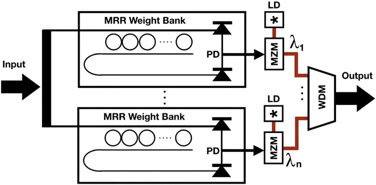
Figure 7. An MRR bank-based broadcast-and-weight protocol. A bundled wavelength is propagated through an MRR bank as it enters. Through the tuning of corresponding rings, each bank weights each wavelength. Photodiodes create photocurrents by adding all wavelengths together. Photo-currents modulate light waves of wavelength λm. Multiplexing of all laser beams is used to broadcast the beams to the next layer. Reproduced with permission, from [148] Mehrabian et al. 2018 © IEEE.
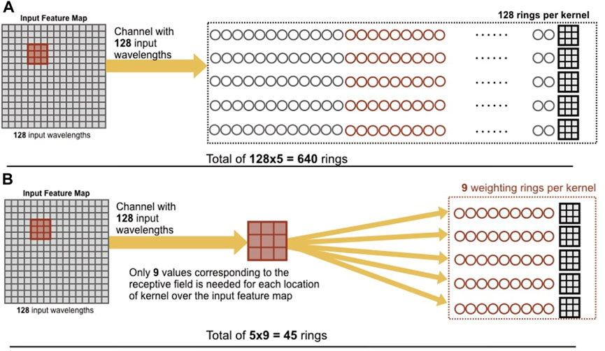
Figure 8. Illustration of MRR bank use in convolution: a 16 × 16 input feature map with 5 kernels of 3 × 3 is implemented in (A) using one ring per input wavelength, whereas (B) uses only one ring per distinct kernel value required to cover the receptive field, which results in fewer required MRRs. Reproduced with permission, from [148], Mehrabian et al. 2018 © IEEE.
Otherwise, the photonic multiplication flow takes place as usual: a waveguide is employed as a transmission line to broadcast multiplexed wavelengths to the next layer, such that each neuron in the destination layer receives all incoming wavelengths. The amplitude of each wavelength at the output is determined by a weighting function corresponding to the incident power and biasing potential of the MRR. Following multiplication, a photodiode integrates all incoming wavelengths, generating an aggregate photocurrent to implement the accumulation operation. With this design, a representative layer of a network such as AlexNet [4] can be evaluated 3 orders of magnitude faster than electronic computation, even including the time cost caused by electronic I/O.
In contrast, it is also possible to implement parallelism along the receptive field dimension. Shiflett et al. take this approach in their Albireo accelerator [143]. In their construction, computation is performed concurrently on multiple receptive fields of the input. The Photonic Locally Connected Units (PLCUs) of Albireo contain a grid of MRRs, where the input dimension is the number of kernel elements represented by MZMs, and the output dimension is the number of receptive fields, each transmitted to an output photodetector. Each PLCU processes a single channel of the convolution, simultaneously computing on all receptive fields. However, to maintain sufficient analog precision, the maximum number of wavelengths for each PLCU is restricted, so to process more fields simultaneously, multiple PLCUs are clustered in PLC groups (PLCGs). Overall, each PLCG implements a single kernel of the layer, acting on the same input volume in parallel, which is broadcast to all PLCGs at the same time. This distributed structure also gives Albireo the ability to implement depth-wise separable convolution layers, which are often used in practice. Albireo illustrates how parallelism is constrained by the number of possible wavelengths, informing design choices based on the expected dimensions of the kernel size, number of kernels, and number of receptive fields in the input.
Optimizations can also be made to balance the overall configuration of the weight banks. Non-coherent architectures are highly susceptible to process variations, as well as runtime variations induced by heat and environmental factors. For instance, increasing the length of the waveguide hosting the MR banks increases the total optical signal propagation, modulation, and losses, which in turn increases the laser power required for optical signals to be detected error-free; crosstalk noise can also substantially deteriorate weight resolution [149]. In their CrossLight accelerator, Sunny et al. [149] perform device-level optimizations to improve robustness. They make adaptations such as hybrid thermo-optic and electro-optic tuning to compensate for thermal crosstalk, and determine an optimal number of MRs per wave bank which can still support 16-bit resolution. They take into consideration layout spacing, wavelength reuse within weight banks, and optical splitter losses. They report that the final optimized configuration has 9.5× lower energy-per-bit and 15.9× higher performance-per-watt over other photonic accelerators.
Sunny et al. introduce another approach to increasing efficiency with SONIC [150], an accelerator architecture optimized for networks that have been compressed using techniques developed in deep learning practice [151]: Figure 9 depicts the SONIC accelerator architecture.. The first compression technique is to apply sparsity-aware training to induce layer-wise sparsity [152]. In the accelerator, sparse and dense vectors can be buffered separately, and the sparse input path uses power gating to prevent VCSELs from being driven for a zero element. The second technique is clustering model weights post-training to restrict to a fixed number of unique weights. This assumption allows for lower resolution requirements in DAC conversion. In SONIC, sparse vector weights can be reduced to 6 bits, while dense activation values are kept at 16 bits. This separation of pathways is reflected in the overall architecture, as shown in Figure 6. These adaptations allow SONIC to improve energy-per-bit 8.4× and power efficiency 5.8× over electronic accelerators.
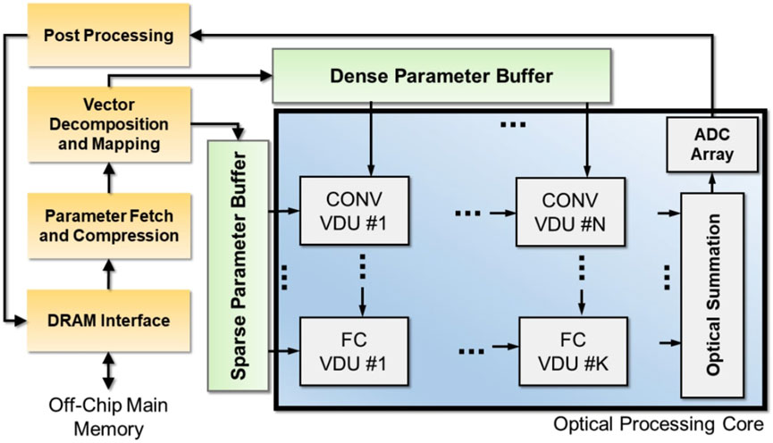
Figure 9. An overview of the SONIC architecture, showing the distinct pathways of data which participates in either sparse or dense computations. Reproduced with permission, from [150], Sunny et al. 2022 © IEEE.
In contrast with analog methods, some accelerators operate in a digital paradigm, using photonic parallelism for concurrent bitwise and logical tasks. An early example within this domain is the HolyLight accelerator, as introduced by Liu et al [45], which is designed to accelerate power-of-2 quantized (P2Q) CNNs [153]. The device incorporates matrix-vector multipliers (MVMs), and a 16-bit ripple-carry adder constructed from full adders using microdisks, alongside P2Q-CNN inference units. This system uses digital electronics to compute the generate and propagate values from the output of each full adder, while the photonic accelerator calculates the sum and carry operations. Two variations of this architecture were developed to explore different aspects of computational efficiency, including the maximum speed of MRR operation, as well as considerations related to noise and signal degradation. HolyLight-M incorporates digital-to-analog converters (DACs) and analog-to-digital converters (ADCs) for the transition between digital values and optical signals. HolyLight-A integrates multiple photonic shifters and adders, connected through a shared bus system. Both variants of HolyLight demonstrate a 5× improvement in power efficiency compared to traditional GPU, CPU, and TPU architectures. Figure 10 shows the overall flow of the accelerator design.
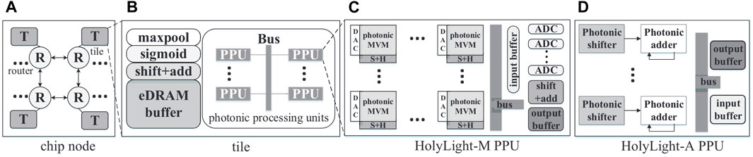
Figure 10. Diagram of the Holylight accelerator architecture [45]. (A) shows the overall chip node, which consists of multiple connected tiles (B). Tiles contain Photonic Processing Units (PPUs). (C) is the PPU structure of the HolyLight-M variant, and (D) is the HolyLight-A PPU. Reproduced with permission from [45], Liu et al. © EDAA.
The PIXEL accelerator of Shiflett et al. [144] is a photonic accelerator that uses a combination of MRRs for bitwise logic operations, and MZMs for accumulation. Mathematically, PIXEL is modeled after the Stripes (STR) [154] formulation of accelerated neural networks through serial-parallel multiplication. In this method, the computational time is linear in the length of the serial input, which is the bit precision of a given network layer. The authors present efficient photonic implementations, with one hybrid Optical-Electrical (OE) version that multiplies in the optical domain and then accumulates in the electrical domain, and a fully Optical-Optical (OO) version for both multiplying and accumulating in the optical domain. PIXEL’s OMAC units use radio frequency memory for storing filter weights in addition to the MAC unit.
In PIXEL, each MZM accumulates a single wavelength, which increases the number of MZMs in their design, reducing area efficiency. Later, Shiflett et al. [155] advanced on the PIXEL design to improve the usage of WDM by implementing parallelism in bit-wise operations. In this design, the bitwise matrix multiplication uses a circulant matrix formulation to take advantage of broadcasting a single bit value to multiple processing elements (PE). The authors again present two versions with different accumulation implementations. In both cases, MRRs are used to implement a bitwise AND operation. The first version then applies electronic processing for summation (O-E-E), while the other uses MZIs for accumulation, with a final electrical summation (O-O-E). The comparison with an all-electronic version of the accelerator shows that the EDP of the O-O-E implementation is 33.1% lower, and its speed is 79.4% faster.
Many accelerators based on logical operations rely on ripple-carry adders and SRAMs, both of which can limit the frequency and inference throughput of the accelerator when trying to replicate higher bit precision, due to the adder’s long critical path and the SRAM’s access latency. Zokaee et al. [156] take a distinct approach to address this problem by processing binarized CNNs rather than CNNs with floating point weights. Their accelerator, LightBulb, uses microdisks to implement XNOR gates and popcount operations, followed by a photonic phase-change memory (pPCM) implementation of ADC. It also reduces input/output latency by using photonic racetrack memory, to enable 50 GHz operating speed. To replace floating-point MACs with XNORs and popcounts, LightBulb first binarizes the weights and activations of a CNN into linear combinations of (−1, + 1)s, allowing the MRR to take advantage of bit-wise parallelism. pPCMs then achieve an ADC step photonically by implementing a temporal binary search [157]. LightBulb compares favorably against state-of-the-art GPU, FPGA, ASIC, ReRAM, and photonic CNN accelerators when tested on binarized MobileNet, ShuffleNet, and ResNet architectures. Overall, LightBulb achieves its efficiency by using photonic components for logical operations, ADC, and data I/O, which are typically large sources of latency and energy overhead. LightBulb improves throughput 17× to 173× over prior optoelectronic accelerators and increases throughput per Watt by 17.5× to 660 ×.
The ROBIN accelerator from Sunny et al. [158] also makes use of binarization, but uses only binarized weights, leaving activation function values at 4-bit precision. This is intended to mitigate loss of accuracy. To implement this, ROBIN uses heterogeneous MRRs with different precisions, within an overall BW-based design, with improved pipelining of interactions with the electronic control unit. ROBIN also implements photonic batch normalization and adds circuit- and device-level optimizations intended to account for the effects of process variations. They perform extensive optimization over device configurations to develop two versions, one optimized for FPS performance (ROBIN-PO), and the other for area and energy efficiency (ROBIN-EO). ROBIN-EO achieves approximately 4x lower energy-per-bit than electronic BNN accelerators, whereas ROBIN-PO shows roughly 3x better performance than electronic BNN accelerators.
Later, Sunny et al. also applied mixed precision to reduce memory requirements with their Heterogeneous Quantization Neural Network Accelerator (HQNNA) [159]. HQNNA uses non-coherent photonics based on both WDM and a novel Time Division Multiplexing (TDM) approach with bit-slicing. The matrix-vector multiplication unit (MVU) performs multiplication and accumulation optically by distributing bit slices across time steps, then using digital shift and adder circuits to produce the final output. Bits that interact in the same dot product are assigned the same wavelength for photonic multiplication and transmitted in one step, with the resulting value shifted and buffered digitally after ADC. This is repeated for the number of bits per slice. This results in performing multiple smaller products rather than a single large product, which improves efficiency given the low latency and energy consumption of photonic multiplication. It also allows for heterogeneous precision across layers. This MVU design is applied both in linear and convolutional layers. HQNNA shows 52.2× and 3.59× improvement in EPB over LightBulb and ROBIN, respectively.
Peng et al. introduced another numerical innovation with DNNARA [160], which combines WDM with a Residue Number System (RNS). With RNS, a number can be represented as pairwise coprime moduli. Because residue arithmetic is digit-irrelevant, results can be combined separately during the residue operation and ensembled at the end, representing addition by mappings in the arithmetic system. Every modulo digit has a single-bit output without repetition, enabling computation-in-network using one-hot encoding photonic routing. RNS can allow for optical components with shorter optical critical paths, and the use of one-hot encoding also facilitates fast switching between the electrical and optical domains. However, the implementation of sigmoid activation functions like logistic and hyperbolic tangent with RNS is difficult. As a result, logistic and tanh functions are approximated by their Taylor series, and they can be implemented as polynomials with adders and multipliers. In subsequent work, the authors introduced DNNARA-E [145], which substitutes DNNARA’s optical adders with electrical adders for reduced area, improved power usage, and ReLU activation function implementation. Overall, this results in three times better throughput than the original DNNARA. With a similar power budget, DNNARA-E achieves on average 80x speedup over the NVIDIA Tesla V100 GPU.
4.2 Beyond convolution
While convolutional neural networks remain an essential area of deep learning, many other architectures are important in practice and contribute to overall deep learning inference usage. This includes architectures that power ChatGPT and other sequence-based tasks, which can be extremely inefficient to evaluate on standard hardware. In addition, many computer vision models are also replacing convolutions with linear layers, as in the Vision Transformer [161]. Recent accelerator designs have begun to address this shift.
Importantly, the Transformer architecture has risen to prominence both in its original context of natural language sequence processing [162], and more recently as a strong alternative in image tasks [161]. To adapt to this trend, Afifi et al. [163] introduced TRON, the first SiPh hardware accelerator for Vision Transformers (ViTs). TRON utilizes non-coherent SiPh circuits to replicate the Transformer architecture’s feedforward and multi-head attention (MHA) units. The required matrix multiplications are performed with an MR weight bank, with a design that efficiently pipelines the operations to re-use intermediate results. The softmax operation is efficiently approximated in the electronic domain, making TRON a hybrid model. TRON also replicates the GELU activation similarly to the method in a standard architecture, scaling the output data vector using an MR, applying a sigmoid function, and then applying MR multiplication again between this output and the data vector. MR units also implement normalization layers, and residual connections are performed through coherent summation. Depending on the application, Transformers may perform encoding only, or both encoding and decoding. TRON is structured so that decoder blocks can re-use the VCSEL arrays which drive input to the MHA unit. This reuse also introduces efficiency by reducing laser power consumption and crosstalk between channels. Figure 11 illustrates this overall structure. Software optimization techniques can also be applied to further reduce the memory footprint of the Transformer for additional performance improvement. TRON is simulated for popular Transformer-based models including BERT [162] and ViT. When compared against state-of-the-art GPU and FPGA accelerators, TRON shows 262× better GOPs than general GPU benchmarks, and 55× improvement over FPGA. It also improves energy-per-bit by 4,231× over GPU, and 8× for FPGA.
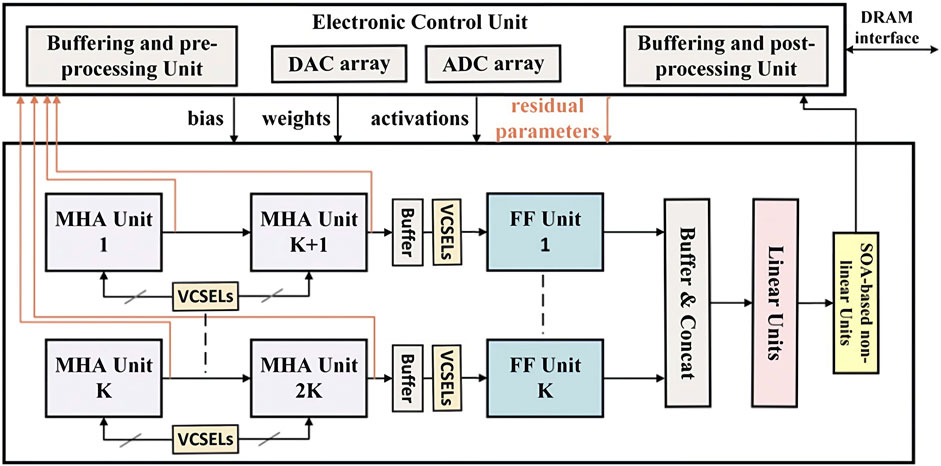
Figure 11. Overview of the TRON accelerator architecture, which replicates the multi-head attention and feedforward blocks of the Transformer architecture. Reproduced with permission, from [163], Afifi et al. 2023, © Association of Computing Machinery.
Another essential class of neural networks is Recurrent Neural Networks (RNNs). Sunny et al. introduced a novel non-coherent photonic RNN accelerator called RecLight [164] which can accelerate NNs that consist of recurrent components, including Gated Recurrent Units (GRUs) and Long Short-Term Memory Networks (LSTMs) [165]. These architectures process sequence data by assigning a trainable “hidden” state to each sequence element. These weight matrices form connections across the sequence. Further, “gating” weights are optimized to either propagate information or suppress unnecessary pathways. To achieve the recurrent network structure, RecLight uses separate MAC units are used for input and hidden state weight matrices. RecLight achieves better parameter resolution by reducing thermal crosstalk, applying a hybrid tuning approach with both thermo-optic (TO) and electro-optic (EO) tuning. When compared with electronic RNN accelerators, RecLight improves energy-per-bit up to 1730×, and has up to 2,631.6× better throughput.
Sarantoglou et al. [166] explore the area of uncertainty quantification and Bayesian networks by introducing an accelerator with two innovative schemes: the first is the Bayesian regularized, aimed at reducing power consumption, and the second is the fully Bayesian, which offers insights into phase shifter sensitivity. Their approach focuses on the MNIST dataset [147] classification with 512 phase shifters, with their architecture similar to the one presented by Perez et al [167]. The system incorporates pre-characterization stages that monitor the variation between the applied current (I) and the induced phase shift (ϕ). These pre-computational steps are designed to counter fabrication errors and inter-element crosstalk through passive offsets. Their findings demonstrate a significant reduction in the processing power required by the photonics integrated Circuit (PIC) without sacrificing classification accuracy. Moreover, the fully Bayesian scheme not only reduces energy consumption but also provides valuable data on phase shifter sensitivity. Consequently, this allows for the partial deactivation of phase actuators, substantially simplifying the driving system. The phase tuning process is based on an offline training scheme that takes into account uncertainty. Instead of defining optimum phase shifter values through training, a parametric Probability Distribution Function (PDF) is defined for each phase shifter and is optimized by updating variational parameters at every iteration. Aside from indicating the correct values for phase shifters, this Bayesian procedure also quantifies their robustness to phase deviation. Using this data, novel algorithms can be developed for adjusting and controlling photonic accelerators, which can further increase their robustness to noise and hence allow for increased scale.
In practice, many modern applications require greater flexibility than a straightforward translation of a network as a unit. To expand the use of photonic accelerators beyond cases that simply apply a fixed architecture, it is essential to develop devices with increased generality. For instance, Demirkiran et al. emphasize the relevance of linear acceleration and efficient matrix multiplication with their ADEPT accelerator [168]. ADEPT addresses important aspects of implementing linear layers, including the fact that most layer transforms are non-square, which can present a performance issue when multiplication and addition are combined in a single optical step. ADEPT favors an optoelectronic architecture combining optical general matrix-matrix multiplication (GEMM) operations with a digital electronic ASIC for nonlinear operations such as activations. In its pipeline, SVD and phase decomposition are performed on the original weights as an up-front digital operation. The design incorporates optimized buffering to minimize the speed bottleneck in optoelectronic transfer. They choose MZI components over MRR, citing their improved compatibility with electronic devices, which can facilitate the integration of the accelerator in practice. ADEPT can accommodate more modes as opposed to other accelerators, illustrating the benefit of a generalized design that can be compared to benchmarks beyond CNN applications. ADEPT shows competitive performance on benchmarks for ResNet-50 [169], BERT-large [162], and RNN-T [170]. They also report 2.5 × better throughput per watt compared to state-of-the-art photonic accelerators.
Li et al. introduced the ASCEND accelerator [171], a chiplet-based system that utilizes the inherent low-latency characteristic of photonic interconnects to facilitate multi-chiplet broadcasting of data and weights within a neural network. This approach leverages the superior speed of optical communications over electrical interconnects [172, 173]. By enabling chiplets to communicate seamlessly, ASCEND minimizes delays in mapping convolution layers both within and across chiplets. The accelerator’s physical layout features columns and rows of local Processing Elements (PEs) organized into unit 2D arrays across chiplets. These PEs communicate with the Global Buffer (GLB) through a waveguide in a unicast manner, while broadcast communication from the GLB to each PE is also facilitated via a waveguide. This arrangement allows for the mapping of convolution layers at the granularity of the 2D PE array, ensuring efficient one-hop communication both within and between chips. ASCEND not only reduces energy consumption by 37% for DenseNet and 67% for ResNet-50 compared to chiplet-based accelerators with metallic interconnects but also achieves up to a 52% improvement in speed. This demonstrates the advantages in energy efficiency and processing speed gained by incorporating diverse photonic elements in accelerator architectures.
4.3 Alternative applications
Another approach focuses on matching the particular strengths of photonics to applications such as edge computing and real-time applications, as well as cases where initial analog-to-digital conversion of input data can be avoided, for a direct pipeline to optical inference. In this area, Sludds et al. introduced Netcast [174], a protocol that employs delocalized analog processing, performing efficient photonics inference using cloud-based smart transceivers to stream weight data to edge devices. This protocol is designed to facilitate the deployment of advanced neural network models on devices with strict power, processing, and memory constraints. Using wavelength division multiplexing (WDM), Netcast uses the optical spectrum for high-capacity data transmission by integrating cloud servers with smart transceivers that broadcast deep neural network weights. Optical matrix-vector multiplication is performed on-site in the edge devices equipped with broadband optical modulators. The weight matrix of one DNN layer is encoded on a time-frequency basis by the amplitude-modulated field. This is streamed to the client, which can modulate it using a broadband optical modulator to separate the wavelengths to N time-integrating detectors to produce the desired dot product. The Netcast design maximizes the number of MACs performed by every component in the client: in effect, this allows it to achieve an efficiency of less than one photon per MAC (0.1 aJ/MAC). Netcast can be readily integrated into applications that operate on data streamed through existing commercial network switches. Through this method, milliwatt-class edge devices can compute at teraFLOPS rates, which were traditionally reserved for cloud computing infrastructures with much larger sizes and power consumption.
In another case, Giamougiannis et al. [175] introduced a coherent analog SiPho computing engine designed for fast optical Tiled Matrix Multiplication (TMM) at 50 GHz. This accelerator incorporates Coherent Linear Neurons (COLNs) equipped with high-speed Silicon Germanium Electro-Absorption Modulators (EAMs) for both weight and input imprinting. The accelerator was deployed in a data center traffic inspection system for network security applications to highlight its practical capabilities in performing TMM. The photonic engine was experimentally tested for identifying Distributed Denial-of-Service (DDoS) attack patterns by classifying Reconnaissance Attacks (RAs). The size of the network is small: only 6 input features, one hidden layer of 8 neurons, and 2-neuron output. However, even this small classifier suffices to solve a practical use-case, demonstrating the advantage of integration into applications where replicating a large network size is not the primary aim.
Another interesting application is demonstrated by the ultra-low-power photonic MindReading accelerator by Lou et al. [176], intended for real-time processing of Electroencephalography (EEG) signals. The EEG device has a sampling rate of 128 Hz, so MindReading seeks to minimize power consumption while matching this rate for inference. To do this, MindReading uses microdisks to perform energy- and area-efficient photonic shifting and adding operations. The accelerator utilizes logarithmic quantization applied to both weights and activations of convolution, recurrent, and fully connected layers. Floating point multiplication is replaced by addition and shift operations with a low bit width requirement so that precision can be reduced to 4 bits with minimal loss in accuracy. This accelerator replicates the structure of EEG-Net, which includes convolutional, fully-connected, and LSTM layers. The LSTM component requires sigmoid (tanh and logistic) activations, so MindReading uses a photonic unit for quantizing these functions. An eDRAM buffer is used for storing EEG signals as well as intermediate results generated by the Photonic Processing Unit (PPU). Then, by using photonic additions and shifters, the PPU computes binary logarithms and logarithmic accumulations for ULQ-quantized EEG-NET. MindReading reduces power consumption by 62.7% and increases throughput by 168.6% on average in comparison to existing accelerator counterparts for the same classification task. Overall, MindReading achieves approximately 1000 IPS (inferences per second) per Watt, whereas FPGA, CPU and GPU can reach less than 5 IPS per Watt.
5 Discussion and research gaps
5.1 Ongoing challenges
Despite the considerable advantages that photonic DL accelerators offer over their electronic counterparts, many challenges persist. In terms of design, the limited scale of PICs still restricts the numerical size of both the input vectors that can be loaded onto photonic hardware and the size and number of internal network layers. Challenges arise when scaling to larger matrices, due to the increasing number of phase shifters in MZI meshes that consume 15 mW on average [99]. The power consumption required for large MAC operations would necessitate thousands of such phase shifters, which increases the cost of thermal management. As an alternative, NOEMS devices have been considered a suitable replacement due to their near-zero static power dissipation as they wiggle the waveguide back and forth [177]. For WDM systems, the in put supported is ultimately limited by the number of wavelength channels that can be multiplexed on a single waveguide bus. However, the number of neurons can be expanded with spectrum reuse techniques for the WDM schemes as reported in [129]. Another challenge to scaling is the implementation of caching memory subsystems, which becomes difficult when handling real workloads generating substantial intermediate data. To execute large-scale neural networks, electronic memories such as SRAM and DRAM can be integrated with optical video memory modules [178].
In the case of coherent approaches, scaling the network can be restricted by the number of required components. Shafiee et al. [179] have conducted an extensive comparison among the Reck, Clements, and Diamond designs to assess their comparative robustness to optical loss and crosstalk noise. This evaluation was carried out by measuring the degradation in inference accuracy with an increased mesh scale. Their work highlights the drawbacks of increasing scale primarily by increasing mesh size. However, advances in PPC design present alternatives where the number of elements in a mesh can be reduced without compromising computational capacity. For instance, in addition to the reduced footprint resulting from a different configuration of components, algorithmic improvements can enhance the fidelity in computing of photonic unitary operation, as shown by Yu and Park [180]. They build on the Clements design by introducing the “pruning” of redundant rotations in the computed operators. The design of Buddhiraju et al. [181] applies a resonator-based architecture utilizing the frequency synthetic dimension, to achieve O(N) scaling in footprint and gate numbers. They report a higher compute density than MZI meshes at approx. 10 TMACs per second per unit area (mm2), which is comparable with silicon crossbar designs. However, the values of N are restricted by the free spectral range of the sources and the device bandwidths. Recent work by Piao et al. [182] focuses on a method that exploits space-time duality for programmable photonic “time” circuits (PPTCs). PPTCs use coupled resonators which substitute spatial optical path length with field evolution in the time domain. This design achieves O(N) scaling in both spatial circuit footprint and the number of optical gates. Other important contributions have also been made to advance error correction mechanisms, mitigating fabrication-induced inaccuracies that compromise the performance of large-scale systems. Bandyopadhyay et al. [183] focuses on improving the fidelity of MZI and mesh-based unitary operations such that, at an application level, developers can assume the underlying hardware will maintain fidelity. Their proposed method involves deterministic correction of hardware errors within optical gates using local corrections. Overall, these examples present interesting possibilities for pushing scale boundaries for PPC-based accelerators.
In the case of MRR-based noncoherent approaches, scaling up can also present problems with increased power requirements and thermal accumulation. Such as nano-optoelectromechanical systems (NOEMS) [184] and liquid crystals on silicon LCOS [67], can notably improve energy efficiency due to the low voltage bias conditions. Efficient weight tuning is achievable with low-loss thermal phase shifters. Moreover, high speed, low voltage swing modulators (1-2 Vpp) [185, 186] promise improved energy efficiency by consuming less power on the CMOS driver and modulator [67]. Other improvements can be achieved using integrated photoconductive heaters [187] with resonant tuning over a wide dynamic range without the need for additional tuning mechanisms or additional electrical interfaces. Integrated with silicon photonics, lithium niobate, and barium titanate electro-optical modulators provide high-speed phase modulation and low operating voltage, making them extremely attractive for photonic accelerators.
In addition to such improvements in the photonic mechanisms, in order to make advances in practical adoption, it is essential to improve standardization in the reporting of design and performance statistics. Comparisons can be hard to make across the literature, as there is limited consistency and completeness in reporting metrics, in terms of hardware and network configurations as well as datasets. Some accelerators do not report inference accuracy, which is a critical statistic considered by deep learning practitioners. It is also crucial to consider that for photonic accelerators to be adopted, they must either integrate seamlessly with existing deep learning platforms such as PyTorch, or present similar user-friendly software libraries where application-level adaptations can be made.
Finally, it is important to note that most accelerators which have been practically implemented still focus on inference with offline training. While this is particularly useful in real-time applications requiring high-speed inference, or edge computing with resource constraints, in practice, the bulk of arithmetic intensity in deep learning is incurred during the training process. Attention has increasingly shifted toward designing accelerators that can execute online photonic training. Buckley et al. [188] provide a recent survey on the status of training capability in PDLAs. Hughes et al. introduced a theoretical treatment considering algorithmic aspects of training in optical platforms [72], and more recently this proposal has been realized experimentally with over 94% accuracy on the MNIST digit recognition task [189]. Free-space devices have been studied by Spall et al. in both hybrid [190] and all-optical [191] variants. Dang et al. have proposed extensions of their ConvLight design which can also accommodate training [192, 193].
Bandyopadhyay et al. [194] have advanced this in the area of PIC by fabricating and testing an all-optical device that performs both inference and in situ training. Their Fully Integrated Coherent Optical Neural Network (FICONN) system incorporates Nonlinear Optical Function Units (NOFUs) and Coherent Matrix Multiplication Units (CMXUs). Taking cues from the proposed forward difference estimation of [72, 127], FICONN demonstrates an advance in efficiency by perturbing all parameters at once in a random direction, rather than individually perturbing the parameters. The system implements a 3-layer DNN and achieves 92.7% test accuracy on vowel classification, comparable to digital computation results on similar tasks. FICONN’s power consumption is dominated by thermal phase shifters, indicating that its performance can be improved even further with more efficient phase shifting units. Observations on the training curve and time to convergence indicate that this area presents a rich potential for comparison with training algorithms in standard hardware.
5.2 Further research
There is much room for research into alternative ways of maximizing the use of photonic components and building improved neural network designs around those novel abilities. Many approaches to date focus on replicating existing neural network architectures, but pushing the boundaries of photonic deep learning will require novel network designs that maximally exploit the strengths of photonics. One important avenue is to rethink the functions that are used within neural networks. Recent work has demonstrated the advantages of architectures that leverage spectral transforms applied globally to input data, particularly successful for PDE and scientific computing applications [195]. Implementing special functions and spectral transforms is more costly in digital hardware, which has so far restricted their utility for large-scale models. However, the inherent properties of photonic devices could make such models more computationally viable [39, 196]. Further, the capacity of MZI meshes for encoding complex-valued operations opens the opportunity for applying complex-valued networks, which have important theoretical advantages but are currently impractical to implement in standard hardware [197].
Another direction is to push the boundaries of device configurations and component optimization through inverse design methods. Improved approaches can for instance enable more advanced design of reconfigurable and tunable components [198, 199]. Recently, researchers have begun to explore the power of machine learning for inverse design. Deep learning shows promise for expanding possibilities in fast, robust, data-driven inverse design, opening the door for free-form approaches [200, 201]. Applying deep learning-enhanced device design methods can, in turn, push the boundaries of what is possible in creating accelerators for deep learning.
Also, on the horizon of photonic accelerators is the field of quantum photonic ML accelerators (QPMLAs). Advances can occur both in the physical layer implementation using quantum memristive (QM) devices and in the improvement of algorithms that run on the application layer of the quantum fabric. A physical realization of a QM photonic system has been reported in [202]. The structure is based on classical photonic devices such as a tunable (dissipative) 50:50 beam splitter and an MZI assembled to realize quantum photonic characteristics without superconducting devices. This technique was adapted for integrated photonics by [203], realizing a reservoir computing model with three photons, nine modes, and three quantum memristors. This glass-based quantum machine was evaluated on both classical and quantum classification tasks, achieving over 95% accuracy, alongside additional capability for detecting quantum entanglement.
Also in the realm of Quantum Optical Neural Networks, Steinbrecher et al. [204] implement a design and observe how natural features of quantum optics can map to the operations of neural networks. They discuss how quantum optics can push beyond simply accelerating classical learning tasks by developing networks which are inherently modeled on quantum states such as coherence and entanglement, which is infeasible in classical computers. This can greatly enhance analysis on physical systems encoded by quantum information. Overall, integrating quantum capabilities into deep learning applications presents an exciting challenge for future developments in network design.
6 Conclusion
Many deep learning operations can be greatly accelerated partially or entirely by photonic devices, allowing for remarkable speed and significantly lower energy consumption compared to their electronic counterparts. The increased compactness and integration density of state-of-the-art on-chip integrated photonics circuits have brought them into the realm of possibility for practical use in artificial neural networks. As shown by the examples in this study, photonic processors can be capable of performing deep learning inference with pre-trained networks at reduced power consumption and enhanced speed. Further, novel designs are even capable of training a model from scratch for end-to-end acceleration. OPUs still face persistent challenges in scalability and integration, and further progress is necessary in more holistic designs which fully integrate hardware, models, and algorithms. By promoting awareness in the deep learning community of the cutting-edge photonics capabilities, and knowledge of practical deep learning considerations in the photonics community, PDLA technology has the potential to circumvent existing resource constraints and expand the boundaries of AI applications.
Author contributions
MA: Conceptualization, Formal Analysis, Investigation, Project administration, Validation, Visualization, Writing–original draft, Writing–review and editing. SP: Writing–review and editing, Conceptualization, Investigation, Visualization. SS: Validation, Visualization, Writing–original draft, Writing–review and editing. MR: Conceptualization, Formal Analysis, Project administration, Supervision, Writing–original draft, Writing–review and editing.
Funding
The author(s) declare that financial support was received for the research, authorship, and/or publication of this article. This work was made possible with the support of the NYUAD Research Enhancement Fund.
Acknowledgments
The authors express their gratitude to the NYU Abu Dhabi Center for Smart Engineering Materials and the Center for Cyber Security for their valuable contributions and support.
Conflict of interest
The authors declare that the research was conducted in the absence of any commercial or financial relationships that could be construed as a potential conflict of interest.
Publisher’s note
All claims expressed in this article are solely those of the authors and do not necessarily represent those of their affiliated organizations, or those of the publisher, the editors and the reviewers. Any product that may be evaluated in this article, or claim that may be made by its manufacturer, is not guaranteed or endorsed by the publisher.
Footnotes
2https://www.lightelligence.ai
4Based on PyTorch library standard implementations, initialized with default weights pulled on 22 March 2024, code using the torchprofile utility on a forward pass of each network on a random tensor of size (32, 3, 224, 224) as a representative input batch size.
References
1. Schmidhuber J. Deep learning in neural networks: an overview. Neural networks (2015) 61:85–117. doi:10.1016/j.neunet.2014.09.003
2. Schmidhuber J. Annotated history of modern AI and deep learning (2022). doi:10.48550/arXiv.2212.11279
3. Moore GE. Progress in digital integrated electronics. In: International electron devices meeting (IEEE) (1975). p. 11–3.
4. Krizhevsky A, Sutskever I, Hinton GE. Imagenet classification with deep convolutional neural networks. Adv Neural Inf Process Syst (2012) 25.
5. Chellapilla K, Puri S, Simard P. High performance convolutional neural networks for document processing. In: Tenth international workshop on frontiers in handwriting recognition (Suvisoft) (2006).
6. Cireşan DC, Meier U, Masci J, Gambardella LM, Schmidhuber J. Flexible, high performance convolutional neural networks for image classification. Proc Twenty-Second Int Jt Conf Artif Intelligence (2011) 2:1237–42.
7. Zhang C, Fang Z, Zhou P, Pan P, Cong J. Caffeine: towards uniformed representation and acceleration for deep convolutional neural networks. In: 2016 IEEE/ACM international conference on computer-aided design (ICCAD). IEEE Press (2016). p. 1–8. doi:10.1145/2966986.2967011
8. Chiou D. The microsoft catapult project. In: 2017 IEEE international symposium on workload characterization (IISWC). IEEE Computer Society (2017). p. 124.
11. Cam E, Hungerford Z, Schoch N, Pinto Miranda F, Yáñez de León CD. Electricity 2024: analysis and forecast to 2026. Tech. rep. International Energy Agency (2024).
12. Xu XY, Jin XM. Integrated photonic computing beyond the von neumann architecture. ACS Photon (2023) 10:1027–36. doi:10.1021/acsphotonics.2c01543
13. Rasras MS, Gill DM, Earnshaw MP, Doerr CR, Weiner JS, Bolle CA, et al. Cmos silicon receiver integrated with ge detector and reconfigurable optical filter. IEEE Photon Tech Lett (2009) 22:112–4. doi:10.1109/lpt.2009.2036590
14. Melloni A, Martinelli M. Synthesis of direct-coupled-resonators bandpass filters for wdm systems. J Lightwave Tech (2002) 20:296–303. doi:10.1109/50.983244
15. Xiao S, Khan MH, Shen H, Qi M. Multiple-channel silicon micro-resonator based filters for wdm applications. Opt Express (2007) 15:7489–98. doi:10.1364/oe.15.007489
16. Cheung S, Su T, Okamoto K, Yoo S. Ultra-compact silicon photonic 512 × 512 25 ghz arrayed waveguide grating router. IEEE J Selected Top Quan Electron (2013) 20:310–6. doi:10.1109/JSTQE.2013.2295879
17. Sorger VJ, Lanzillotti-Kimura ND, Ma RM, Zhang X. Ultra-compact silicon nanophotonic modulator with broadband response. Nanophotonics (2012) 1:17–22. doi:10.1515/nanoph-2012-0009
18. Timurdogan E, Sorace-Agaskar CM, Sun J, Shah Hosseini E, Biberman A, Watts MR. An ultralow power athermal silicon modulator. Nat Commun (2014) 5:4008–11. doi:10.1038/ncomms5008
19. Sepehrian H, Lin J, Rusch LA, Shi W. Silicon photonic iq modulators for 400 gb/s and beyond. J Lightwave Tech (2019) 37:3078–86. doi:10.1109/jlt.2019.2910491
20. Rosenberg J, Green W, Assefa S, Gill D, Barwicz T, Yang M, et al. A 25 gbps silicon microring modulator based on an interleaved junction. Opt express (2012) 20:26411–23. doi:10.1364/oe.20.026411
21. Ban Y, Verbist J, Vanhoecke M, Bauwelinck J, Verheyen P, Lardenois S, et al. Low-voltage 60gb/s nrz and 100gb/s pam4 o-band silicon ring modulator. In: 2019 IEEE optical interconnects conference (OI) (IEEE) (2019). p. 1–2.
22. Javidi B, Li J, Tang Q. Optical implementation of neural networks for face recognition by the use of nonlinear joint transform correlators. Appl Opt (1995) 34:3950–62. doi:10.1364/ao.34.003950
23. Javidi B. Comparison of nonlinear joint transform correlator and nonlinearly transformed matched filter based correlator for noisy input scenes. Opt Eng (1990) 29:1013–20. doi:10.1117/12.55703
24. Reck M, Zeilinger A, Bernstein HJ, Bertani P. Experimental realization of any discrete unitary operator. Phys Rev Lett (1994) 73:58–61. doi:10.1103/physrevlett.73.58
25. Miller DA. Establishing optimal wave communication channels automatically. J Lightwave Tech (2013) 31:3987–94. doi:10.1109/jlt.2013.2278809
26. Miller DA. Self-aligning universal beam coupler. Opt express (2013) 21:6360–70. doi:10.1364/oe.21.006360
28. Clements WR, Humphreys PC, Metcalf BJ, Kolthammer WS, Walmsley IA. Optimal design for universal multiport interferometers. Optica (2016) 3:1460–5. doi:10.1364/OPTICA.3.001460
29. Miller DA. Reconfigurable add-drop multiplexer for spatial modes. Opt express (2013) 21:20220–9. doi:10.1364/oe.21.020220
30. Hardy J, Shamir J. Optics inspired logic architecture. Opt Express (2007) 15:150–65. doi:10.1364/oe.15.000150
31. Schwelb O. Transmission, group delay, and dispersion in single-ring optical resonators and add/drop filters-a tutorial overview. J Lightwave Tech (2004) 22:1380–94. doi:10.1109/jlt.2004.827666
32. Xu Q, Shakya J, Lipson M. Direct measurement of tunable optical delays on chip analogue to electromagnetically induced transparency. Opt express (2006) 14:6463–8. doi:10.1364/oe.14.006463
33. Xu Q, Fattal D, Beausoleil RG. Silicon microring resonators with 1.5-μm radius. Opt express (2008) 16:4309–15. doi:10.1364/oe.16.004309
34. Zhang L, Ji R, Jia L, Yang L, Zhou P, Tian Y, et al. Demonstration of directed xor/xnor logic gates using two cascaded microring resonators. Opt Lett (2010) 35:1620–2. doi:10.1364/ol.35.001620
35. Wu C, Yu H, Lee S, Peng R, Takeuchi I, Li M. Programmable phase-change metasurfaces on waveguides for multimode photonic convolutional neural network. Nat Commun (2021) 12:96. doi:10.1038/s41467-020-20365-z
36. Tamalampudi SR, Dushaq G, Villegas JE, Rajput NS, Paredes B, Elamurugu E, et al. Short-wavelength infrared (swir) photodetector based on multi-layer 2d gagete. Opt Express (2021) 29:39395–405. doi:10.1364/oe.442845
37. Dushaq G, Paredes B, Villegas JE, Tamalampudi SR, Rasras M. On-chip integration of 2d van der waals germanium phosphide (gep) for active silicon photonics devices. Opt Express (2022) 30:15986–97. doi:10.1364/oe.457242
38. Tamalampudi SR, Dushaq G, Villegas JE, Paredes B, Rasras MS. A multi-layered gagete electro-optic device integrated in silicon photonics. J Lightwave Tech (2023) 1–7. doi:10.1109/jlt.2023.3237818
39. Serunjogi SM, Sanduleanu MA, Rasras MS. Volterra series based linearity analysis of a phase-modulated microwave photonic link. J Lightwave Tech (2017) 36:1537–51. doi:10.1109/JLT.2017.2782886
40. Psaltis D, Brady D, Wagner K. Adaptive optical networks using photorefractive crystals. Appl Opt (1988) 27:1752–9. doi:10.1364/ao.27.001752
41. Farhat NH, Psaltis D, Prata A, Paek E. Optical implementation of the Hopfield model. Appl Opt (1985) 24:1469. doi:10.1364/AO.24.001469
42. Ito F, Ki K. Optical implementation of the Hopfield neural network using multiple fiber nets. Appl Opt (1989) 28:4176. doi:10.1364/AO.28.004176
43. Choquette J, Gandhi W, Giroux O, Stam N, Krashinsky R. Nvidia a100 tensor core gpu: performance and innovation. IEEE Micro (2021) 41:29–35. doi:10.1109/mm.2021.3061394
45. Liu W, Liu W, Ye Y, Lou Q, Xie Y, Jiang L. Holylight: a nanophotonic accelerator for deep learning in data centers. In: 2019 design, automation & test in europe conference & exhibition (DATE) (2019). p. 1483–8. doi:10.23919/DATE.2019.8715195
46. Fujiwara H, Mori H, Zhao WC, Chuang MC, Naous R, Chuang CK, et al. A 5-nm 254-tops/w 221-tops/mm 2 fully-digital computing-in-memory macro supporting wide-range dynamic-voltage-frequency scaling and simultaneous mac and write operations. In: 2022 IEEE international solid-state circuits conference (ISSCC) (IEEE), 65 (2022). p. 1–3. doi:10.1109/isscc42614.2022.9731754
47. Mori H, Zhao WC, Lee CE, Lee CF, Hsu YH, Chuang CK, et al. A 4nm 6163-tops/w/b 4790 − TOPS/mm2/b sram based digital-computing-in-memory macro supporting bit-width flexibility and simultaneous mac and weight update. In: 2023 IEEE international solid-state circuits conference (ISSCC) (IEEE) (2023). p. 132–4.
48. Farmakidis N, Youngblood N, Li X, Tan J, Swett JL, Cheng Z, et al. Plasmonic nanogap enhanced phase-change devices with dual electrical-optical functionality. Sci Adv (2019) 5:eaaw2687. doi:10.1126/sciadv.aaw2687
49. Zhang H, Zhou L, Lu L, Xu J, Wang N, Hu H, et al. Miniature multilevel optical memristive switch using phase change material. ACS Photon (2019) 6:2205–12. doi:10.1021/acsphotonics.9b00819
50. Feldmann J, Youngblood N, Li X, Wright CD, Bhaskaran H, Pernice WH. Integrated 256 cell photonic phase-change memory with 512-bit capacity. IEEE J Selected Top Quan Electron (2019) 26:1–7. doi:10.1109/jstqe.2019.2956871
51. Tait AN, Wu AX, De Lima TF, Zhou E, Shastri BJ, Nahmias MA, et al. Microring weight banks. IEEE J Selected Top Quan Electron (2016) 22:312–25. doi:10.1109/jstqe.2016.2573583
52. Zhou W, Farmakidis N, Feldmann J, Li X, Tan J, He Y, et al. Phase-change materials for energy-efficient photonic memory and computing. MRS Bull (2022) 47:502–10. doi:10.1557/s43577-022-00358-7
53. Miscuglio M, Adam GC, Kuzum D, Sorger VJ. Roadmap on material-function mapping for photonic-electronic hybrid neural networks. APL Mater (2019) 7. doi:10.1063/1.5109689
54. Ma X, Meng J, Peserico N, Miscuglio M, Zhang Y, Hu J, et al. Photonic tensor core with photonic compute-in-memory. In: Optical fiber communication conference. Optica Publishing Group (2022). p. M2E–4.
55. Peserico N, Ma X, Shastri BJ, Sorger VJ. Photonic tensor core for machine learning: a review. In: Emerging topics in artificial intelligence (ETAI) 2022 12204 (2022). p. 53–60.
56. Ríos C, Youngblood N, Cheng Z, Le Gallo M, Pernice WH, Wright CD, et al. In-memory computing on a photonic platform. Sci Adv (2019) 5:eaau5759. doi:10.1126/sciadv.aau5759
57. Wu C, Lee S, Yu H, Peng R, Takeuchi I, Li M. Programmable phase-change metasurface for multimode photonic convolutional neural network. In: 2020 IEEE photonics conference (IPC) (IEEE) (2020). p. 1–2.
58. Cheng Z, Ríos C, Youngblood N, Wright CD, Pernice WH, Bhaskaran H. Device-level photonic memories and logic applications using phase-change materials. Adv Mater (2018) 30:1802435. doi:10.1002/adma.201802435
59. Zhang Y, Chou JB, Li J, Li H, Du Q, Yadav A, et al. Broadband transparent optical phase change materials for high-performance nonvolatile photonics. Nat Commun (2019) 10:4279. doi:10.1038/s41467-019-12196-4
60. Sebastian A, Le Gallo M, Burr GW, Kim S, BrightSky M, Eleftheriou E. Tutorial: brain-inspired computing using phase-change memory devices. J Appl Phys (2018) 124. doi:10.1063/1.5042413
61. Ambrogio S, Narayanan P, Tsai H, Shelby RM, Boybat I, Di NC, et al. Equivalent-accuracy accelerated neural-network training using analogue memory. Nature (2018) 558:60–7. doi:10.1038/s41586-018-0180-5
62. Farquhar E, Hasler P. A bio-physically inspired silicon neuron. IEEE Trans Circuits Syst Regular Pap (2005) 52:477–88. doi:10.1109/tcsi.2004.842871
63. Szilagyi L, Pliva J, Henker R, Schoeniger D, Turkiewicz JP, Ellinger F. A 53-gbit/s optical receiver frontend with 0.65 pj/bit in 28-nm bulk-cmos. IEEE J Solid-State Circuits (2018) 54:845–55. doi:10.1109/jssc.2018.2885531
64. Stroev N, Berloff NG. Analog photonics computing for information processing, inference, and optimization. Adv Quan Tech (2023) 6:2300055. doi:10.1002/qute.202300055
65. Huang C, Sorger VJ, Miscuglio M, Al-Qadasi M, Mukherjee A, Lampe L, et al. Prospects and applications of photonic neural networks. Adv Phys X (2022) 7:1981155. doi:10.1080/23746149.2021.1981155
66. Wu J, Lin X, Guo Y, Liu J, Fang L, Jiao S, et al. Analog optical computing for artificial intelligence. Engineering (2022) 10:133–45. doi:10.1016/j.eng.2021.06.021
67. Al-Qadasi M, Chrostowski L, Shastri B, Shekhar S. Scaling up silicon photonic-based accelerators: challenges and opportunities. APL Photon (2022) 7. doi:10.1063/5.0070992
68. Xia C, Chen Y, Zhang H, Zhang H, Wu J. Photonic computing and communication for neural network accelerators. In: International conference on parallel and distributed computing: applications and technologies. Springer (2021). p. 121–8.
69. Ma X, Peserico N, Khaled A, Guo Z, Nouri B, Dalir H, et al. High-density integrated photonic tensor processing unit with a matrix multiply compiler (2022).
70. Launay J, Poli I, Müller K, Carron I, Daudet L, Krzakala F, et al. Light-in-the-loop: using a photonics co-processor for scalable training of neural networks (2020). arXiv preprint arXiv:2006.01475.
71. Hesslow D, Cappelli A, Carron I, Daudet L, Lafargue R, Müller K, et al. Photonic co-processors in hpc: using lighton opus for randomized numerical linear algebra (2021). arXiv preprint arXiv:2104.14429.
72. Hughes TW, Minkov M, Shi Y, Fan S. Training of photonic neural networks through in situ backpropagation and gradient measurement. Optica (2018) 5:864–71. doi:10.1364/optica.5.000864
73. Brossollet C, Cappelli A, Carron I, Chaintoutis C, Chatelain A, Daudet L, et al. Lighton optical processing unit: Scaling-up ai and hpc with a non von neumann co-processor (2021). arXiv preprint arXiv:2107.11814.
75. Burr GW, Brightsky MJ, Sebastian A, Cheng HY, Wu JY, Kim S, et al. Recent progress in phase-change memory technology. IEEE J Emerging Selected Top Circuits Syst (2016) 6:146–62.
76. Harris NC, Carolan J, Bunandar D, Prabhu M, Hochberg M, Baehr-Jones T, et al. Linear programmable nanophotonic processors. Optica (2018) 5:1623–31. doi:10.1364/OPTICA.5.001623
77. Bogaerts W, Pérez D, Capmany J, Miller DA, Poon J, Englund D, et al. Programmable photonic circuits. Nature (2020) 586:207–16. doi:10.1038/s41586-020-2764-0
78. Li X, Youngblood N, Ríos C, Cheng Z, Wright CD, Pernice WH, et al. Fast and reliable storage using a 5 bit, nonvolatile photonic memory cell. Optica (2019) 6:1–6. doi:10.1364/optica.6.000001
79. Xu P, Zheng J, Doylend JK, Majumdar A. Low-loss and broadband nonvolatile phase-change directional coupler switches. Acs Photon (2019) 6:553–7. doi:10.1021/acsphotonics.8b01628
80. Wuttig M, Bhaskaran H, Taubner T. Phase-change materials for non-volatile photonic applications. Nat Photon (2017) 11:465–76. doi:10.1038/nphoton.2017.126
81. Yang Z, Ramanathan S. Breakthroughs in photonics 2014: phase change materials for photonics. IEEE Photon J (2015) 7:1–5. doi:10.1109/jphot.2015.2413594
82. Xu Q, Soref R. Reconfigurable optical directed-logic circuits using microresonator-based optical switches. Opt Express (2011) 19:5244–59. doi:10.1364/oe.19.005244
83. Luo W, Cao L, Shi Y, Wan L, Zhang H, Li S, et al. Recent progress in quantum photonic chips for quantum communication and internet. Light: Sci Appl (2023) 12:175. doi:10.1038/s41377-023-01173-8
84. Paraiso TK, Roger T, Marangon DG, De Marco I, Sanzaro M, Woodward RI, et al. A photonic integrated quantum secure communication system. Nat Photon (2021) 15:850–6. doi:10.1038/s41566-021-00873-0
85. Litvin A, Martynenko I, Purcell-Milton F, Baranov A, Fedorov A, Gun’Ko Y. Colloidal quantum dots for optoelectronics. J Mater Chem A (2017) 5:13252–75. doi:10.1039/c7ta02076g
86. Tate N. Quantum-dot-based photonic reservoir computing. In: Photonic neural networks with spatiotemporal dynamics (2024). p. 71.
87. Lingnau B, Perrott AH, Dernaika M, Caro L, Peters FH, Kelleher B. Dynamics of on-chip asymmetrically coupled semiconductor lasers. Opt Lett (2020) 45:2223–6. doi:10.1364/ol.390401
88. Shainline JM, Buckley SM, Mirin RP, Nam SW. Superconducting optoelectronic circuits for neuromorphic computing. Phys Rev Appl (2017) 7:034013. doi:10.1103/physrevapplied.7.034013
89. Wang J, Paesani S, Ding Y, Santagati R, Skrzypczyk P, Salavrakos A, et al. Multidimensional quantum entanglement with large-scale integrated optics. Science (2018) 360:285–91. doi:10.1126/science.aar7053
90. Politi A, Matthews JC, O’Brien JL. Shor’s quantum factoring algorithm on a photonic chip. Science (2009) 325:1221. doi:10.1126/science.1173731
91. Zhou XQ, Kalasuwan P, Ralph TC, O’brien JL. Calculating unknown eigenvalues with a quantum algorithm. Nat Photon (2013) 7:223–8. doi:10.1038/nphoton.2012.360
92. Qiang X, Wang Y, Xue S, Ge R, Chen L, Liu Y, et al. Implementing graph-theoretic quantum algorithms on a silicon photonic quantum walk processor. Sci Adv (2021) 7:eabb8375. doi:10.1126/sciadv.abb8375
93. Wang J, Sciarrino F, Laing A, Thompson MG. Integrated photonic quantum technologies. Nat Photon (2020) 14:273–84. doi:10.1038/s41566-019-0532-1
94. Hsu CY, Yiu GZ, Chang YC. Free-space applications of silicon photonics: a review. Micromachines (2022) 13:990. doi:10.3390/mi13070990
95. Zhu W, Zhang L, Lu Y, Zhou P, Yang L. Design and experimental verification for optical module of optical vector–matrix multiplier. Appl Opt (2013) 52:4412–8. doi:10.1364/ao.52.004412
96. Fontaine NK, Ryf R, Chen H, Neilson DT, Kim K, Carpenter J. Laguerre-Gaussian mode sorter. Nat Commun (2019) 10:1865. doi:10.1038/s41467-019-09840-4
97. Lin X, Rivenson Y, Yardimci NT, Veli M, Luo Y, Jarrahi M, et al. All-optical machine learning using diffractive deep neural networks. Science (2018) 361:1004–8. doi:10.1126/science.aat8084
98. Hamerly R, Bernstein L, Sludds A, Soljačić M, Englund D. Large-scale optical neural networks based on photoelectric multiplication. Phys Rev X (2019) 9:021032. doi:10.1103/physrevx.9.021032
99. Zhou H, Dong J, Cheng J, Dong W, Huang C, Shen Y, et al. Photonic matrix multiplication lights up photonic accelerator and beyond. Light: Sci Appl (2022) 11:30. doi:10.1038/s41377-022-00717-8
100. Zhou T, Lin X, Wu J, Chen Y, Xie H, Li Y, et al. Large-scale neuromorphic optoelectronic computing with a reconfigurable diffractive processing unit. Nat Photon (2021) 15:367–73. doi:10.1038/s41566-021-00796-w
101. Cordaro A, Edwards B, Nikkhah V, Alù A, Engheta N, Polman A. Solving integral equations in free space with inverse-designed ultrathin optical metagratings. Nat Nanotechnology (2023) 18:365–72. doi:10.1038/s41565-022-01297-9
102. Li M, Deng Y, Tang J, Sun S, Yao J, Azaña J, et al. Reconfigurable optical signal processing based on a distributed feedback semiconductor optical amplifier. Scientific Rep (2016) 6:19985. doi:10.1038/srep19985
103. Tanaka G, Yamane T, Héroux JB, Nakane R, Kanazawa N, Takeda S, et al. Recent advances in physical reservoir computing: a review. Neural Networks (2019) 115:100–23. doi:10.1016/j.neunet.2019.03.005
104. Paquot Y, Duport F, Smerieri A, Dambre J, Schrauwen B, Haelterman M, et al. Optoelectronic reservoir computing. Scientific Rep (2012) 2:287. doi:10.1038/srep00287
105. Vandoorne K, Dambre J, Verstraeten D, Schrauwen B, Bienstman P. Parallel reservoir computing using optical amplifiers. IEEE Trans Neural networks (2011) 22:1469–81. doi:10.1109/tnn.2011.2161771
106. Larger L, Soriano MC, Brunner D, Appeltant L, Gutiérrez JM, Pesquera L, et al. Photonic information processing beyond turing: an optoelectronic implementation of reservoir computing. Opt express (2012) 20:3241–9. doi:10.1364/oe.20.003241
107. Nakajima M, Tanaka K, Hashimoto T. Scalable reservoir computing on coherent linear photonic processor. Commun Phys (2021) 4:20. doi:10.1038/s42005-021-00519-1
108. Pelucchi E, Fagas G, Aharonovich I, Englund D, Figueroa E, Gong Q, et al. The potential and global outlook of integrated photonics for quantum technologies. Nat Rev Phys (2022) 4:194–208. doi:10.1038/s42254-021-00398-z
109. Sibson P, Kennard JE, Stanisic S, Erven C, O’Brien JL, Thompson MG. Integrated silicon photonics for high-speed quantum key distribution. Optica (2017) 4:172–7. doi:10.1364/optica.4.000172
110. Buck S, Coleman R, Sargsyan H. Continuous variable quantum algorithms: an introduction (2021). arXiv preprint arXiv:2107.02151.
111. Bunandar D, Lentine A, Lee C, Cai H, Long CM, Boynton N, et al. Metropolitan quantum key distribution with silicon photonics. Phys Rev X (2018) 8:021009. doi:10.1103/physrevx.8.021009
112. Ying Z, Feng C, Zhao Z, Dhar S, Dalir H, Gu J, et al. Electronic-photonic arithmetic logic unit for high-speed computing. Nat Commun (2020) 11:2154. doi:10.1038/s41467-020-16057-3
113. Ying Z, Feng C, Zhao Z, Gu J, Soref R, Pan DZ, et al. Sequential logic and pipelining in chip-based electronic-photonic digital computing. IEEE Photon J (2020) 12:1–11. doi:10.1109/jphot.2020.3031641
114. Gostimirovic D, Ye WN. Ultracompact cmos-compatible optical logic using carrier depletion in microdisk resonators. Scientific Rep (2017) 7:12603. doi:10.1038/s41598-017-12680-1
115. Lei L, Dong J, Zhang Y, He H, Yu Y, Zhang X. Reconfigurable photonic full-adder and full-subtractor based on three-input xor gate and logic minterms. Electron Lett (2012) 48:399–400. doi:10.1049/el.2012.0493
116. Lu GW, Qin J, Wang H, Ji X, Sharif GM, Yamaguchi S. Flexible and re-configurable optical three-input xor logic gate of phase-modulated signals with multicast functionality for potential application in optical physical-layer network coding. Opt express (2016) 24:2299–306. doi:10.1364/oe.24.002299
117. Ying Z, Dhar S, Zhao Z, Feng C, Mital R, Chung CJ, et al. Electro-optic ripple-carry adder in integrated silicon photonics for optical computing. IEEE J Selected Top Quan Electron (2018) 24:1–10. doi:10.1109/JSTQE.2018.2836955
118. Rostami A, Nejad HBA, Qartavol RM, Saghai HR. Tb/s optical logic gates based on quantum-dot semiconductor optical amplifiers. IEEE J Quan Electron (2010) 46:354–60. doi:10.1109/JQE.2009.2033253
119. Mukherjee K. Ultra-fast and gate using single semi-reflective quantum dot semiconductor optical amplifier. Photonic Netw Commun (2023) 45:97–106. doi:10.1007/s11107-023-00996-0
120. Rostami A, Nejad HBA, Qartavol RM, Saghai HR. Tb/s optical logic gates based on quantum-dot semiconductor optical amplifiers. IEEE J Quan Electron (2010) 46:354–60. doi:10.1109/jqe.2009.2033253
121. Zhang M, Wang L, Ye P. All optical xor logic gates: technologies and experiment demonstrations. IEEE Commun Mag (2005) 43:S19–S24. doi:10.1109/mcom.2005.1453421
122. Cybenko G. Approximation by superpositions of a sigmoidal function. Maths Control Signals Syst (1989) 2:303–14. doi:10.1007/BF02551274
123. Benth FE, Detering N, Galimberti L. Neural networks in Fréchet spaces. Ann Maths Artif Intelligence (2023) 91:75–103. doi:10.1007/s10472-022-09824-z
124. Simonyan K, Zisserman A. Very deep convolutional networks for large-scale image recognition (2015).
125. Anderson A, Vasudevan A, Keane C, Gregg D. High-performance low-memory lowering: gemm-based algorithms for dnn convolution. In: 2020 IEEE 32nd international symposium on computer architecture and high performance computing (SBAC-PAD) (2020). p. 99–106. doi:10.1109/SBAC-PAD49847.2020.00024
126. Vasudevan A, Anderson A, Gregg D. Parallel multi channel convolution using general matrix multiplication. In: 2017 IEEE 28th international conference on application-specific systems, architectures and processors (ASAP). Los Alamitos, CA, USA: IEEE Computer Society (2017). p. 19–24. doi:10.1109/ASAP.2017.7995254
127. Shen Y, Harris NC, Skirlo S, Prabhu M, Baehr-Jones T, Hochberg M, et al. Deep learning with coherent nanophotonic circuits. Nat Photon (2017) 11:441–6. doi:10.1109/phosst.2017.8012714
128. Shokraneh F, Geoffroy-gagnon S, Liboiron-Ladouceur O. The diamond mesh, a phase-error- and loss-tolerant field-programmable MZI-based optical processor for optical neural networks. Opt Express (2020) 28:23495–508. doi:10.1364/OE.395441
129. Tait AN, Nahmias MA, Shastri BJ, Prucnal PR. Broadcast and weight: an integrated network for scalable photonic spike processing. J Lightwave Tech (2014) 32:4029–41. doi:10.1109/jlt.2014.2345652
130. Feldmann J, Youngblood N, Karpov M, Gehring H, Li X, Stappers M, et al. Parallel convolutional processing using an integrated photonic tensor core. Nature (2021) 589:52–8. doi:10.1038/s41586-020-03070-1
131. Xea X, Tan M, Corcoran B, Wu J, Boes A, Nguyen TG, et al. 11tops photonic convolutional accelerator for optical neural networks. Nature (2021) 589:44–51. doi:10.1038/s41586-020-03063-0
132. Ashtiani F, On MB, Sanchez-Jacome D, Perez-Lopez D, Ben Yoo SJ, Blanco-Redondo A. Photonic max-pooling for deep neural networks using a programmable photonic platform. In: 2023 optical fiber communications conference and exhibition (OFC) (2023). p. 1–3. doi:10.1364/OFC.2023.M1J.6
133. Marinis LD, Nesti F, Cococcioni M, Andriolli N. A photonic accelerator for feature map generation in convolutional neural networks. OSA Advanced Photonics Congress (AP) 2020 (IPR, NP, NOMA, Networks, PVLED, PSC, SPPCom, SOF). Optica Publishing Group (2020). doi:10.1364/PSC.2020.PsTh1F.3
134. Chua L. Memristor-the missing circuit element. IEEE Trans Circuit Theor (1971) 18:507–19. doi:10.1109/TCT.1971.1083337
135. Xia Q, Yang JJ. Memristive crossbar arrays for brain-inspired computing. Nat Mater (2019) 18:309–23. doi:10.1038/s41563-019-0291-x
136. Shafiee A, Nag A, Muralimanohar N, Balasubramonian R, Strachan JP, Hu M, et al. Isaac: a convolutional neural network accelerator with in-situ analog arithmetic in crossbars. In: 2016 ACM/IEEE 43rd annual international symposium on computer architecture (ISCA) (2016). p. 14–26.
137. Mao JY, Zhou L, Zhu X, Zhou Y, Han ST. Photonic memristor for future computing: a perspective. Adv Opt Mater (2019) 7:1900766. doi:10.1002/adom.201900766
138. Choi S, Kim J, Kwak J, Park N, Yu S. Topologically protected all-optical memory. Adv Electron Mater (2022) 8:2200579. doi:10.1002/aelm.202200579
139. Nahmias MA, de Lima TF, Tait AN, Peng HT, Shastri BJ, Prucnal PR. Photonic multiply-accumulate operations for neural networks. IEEE J Selected Top Quan Electron (2020) 26:1–18. doi:10.1109/JSTQE.2019.2941485
140. Miscuglio M, Sorger VJ. Photonic tensor cores for machine learning. Appl Phys Rev (2020) 7. doi:10.1063/5.0001942
141. Strassen V. Gaussian elimination is not optimal. Numerische Mathematik (1969) 13:354–6. doi:10.1007/BF02165411
142. Coppersmith D, Winograd S. Matrix multiplication via arithmetic progressions. J Symbolic Comput (1990) 9:251–80. doi:10.1016/S0747-7171(08)80013-2
143. Shiflett K, Karanth A, Bunescu R, Louri A. Albireo: energy-efficient acceleration of convolutional neural networks via silicon photonics. In: 2021 ACM/IEEE 48th annual international symposium on computer architecture (ISCA) (IEEE) (2021). p. 860–73.
144. Shiflett K, Wright D, Karanth A, Louri A. Pixel: photonic neural network accelerator. In: 2020 IEEE international symposium on high performance computer architecture (HPCA) (IEEE) (2020). p. 474–87.
145. Peng J, Alkabani Y, Puri K, Ma X, Sorger V, El-Ghazawi T. A deep neural network accelerator using residue arithmetic in a hybrid optoelectronic system. ACM J Emerging Tech Comput Syst (Jetc) (2022) 18:1–26. doi:10.1145/3550273
146. Dang D, Dass J, Mahapatra R. Convlight: a convolutional accelerator with memristor integrated photonic computing. In: 2017 IEEE 24th international conference on high performance computing (HiPC). IEEE (2017). p. 114–23.
147. Deng L. The mnist database of handwritten digit images for machine learning research. IEEE Signal Process. Mag (2012) 29:141–2.
148. Mehrabian A, Al-Kabani Y, Sorger VJ, El-Ghazawi T. Pcnna: a photonic convolutional neural network accelerator. In: 2018 31st IEEE international system-on-chip conference (SOCC) (IEEE) (2018). p. 169–73.
149. Sunny F, Mirza A, Nikdast M, Pasricha S. Crosslight: a cross-layer optimized silicon photonic neural network accelerator. In: 2021 58th ACM/IEEE design automation conference (DAC) (2021). p. 1069–74. doi:10.1109/DAC18074.2021.9586161
150. Sunny F, Nikdast M, Pasricha S. Sonic: a sparse neural network inference accelerator with silicon photonics for energy-efficient deep learning. In: 2022 27th asia and south pacific design automation conference (ASP-DAC) (2022). p. 214–9. doi:10.1109/ASP-DAC52403.2022.9712530
151. Han S, Mao H, Dally WJ. Deep compression: compressing deep neural networks with pruning. In: Trained quantization and huffman coding (2016). doi:10.48550/arXiv.1510.00149
152. Zhu MH, Gupta S. To prune, or not to prune: exploring the efficacy of pruning for model compression (2018).
153. Zhou A, Yao A, Guo Y, Xu L, Chen Y. Incremental network quantization: towards lossless CNNs with low-precision weights. In: International conference on learning representations (2017).
154. Judd P, Albericio J, Hetherington T, Aamodt TM, Moshovos A. Stripes: bit-serial deep neural network computing. In: 2016 49th annual IEEE/ACM international symposium on microarchitecture (MICRO) (2016). p. 1–12. doi:10.1109/MICRO.2016.7783722
155. Shiflett K, Karanth A, Louri A, Bunescu R. Bitwise neural network acceleration using silicon photonics. In: Proceedings of the 2021 on great lakes symposium on VLSI (2021). p. 9–14.
156. Zokaee F, Lou Q, Youngblood N, Liu W, Xie Y, Jiang L. Lightbulb: a photonic-nonvolatile-memory-based accelerator for binarized convolutional neural networks. In: 2020 design, automation & test in europe conference & exhibition (DATE) (IEEE) (2020). p. 1438–43.
157. Danial L, Wainstein N, Kraus S, Kvatinsky S. Breaking through the speed-power-accuracy tradeoff in ADCs using a memristive neuromorphic architecture. IEEE Trans Emerging Top Comput Intelligence (2018) 2:396–409. doi:10.1109/TETCI.2018.2849109
158. Sunny FP, Mirza A, Nikdast M, Pasricha S. Robin: a robust optical binary neural network accelerator (2021). doi:10.1145/3476988
159. Sunny F, Nikdast M, Pasricha S. A silicon photonic accelerator for convolutional neural networks with heterogeneous quantization. In: Proceedings of the great lakes symposium on VLSI 2022 (2022). p. 367–71.
160. Peng J, Alkabani Y, Sun S, Sorger VJ, El-Ghazawi T. Dnnara: a deep neural network accelerator using residue arithmetic and integrated photonics. In: Proceedings of the 49th international conference on parallel processing (2020). p. 1–11.
161. Dosovitskiy A, Beyer L, Kolesnikov A, Weissenborn D, Zhai X, Unterthiner T, et al. An image is worth 16x16 words: Transformers for image recognition at scale (2020). CoRR abs/2010.11929.
162. Devlin J, Chang MW, Lee K, Toutanova K. BERT: pre-training of deep bidirectional Transformers for language understanding. In: J Burstein, C Doran, and T Solorio, editors. Proceedings of the 2019 conference of the north American chapter of the association for computational linguistics: human language technologies, volume 1 (long and Short papers). Minneapolis, Minnesota: Association for Computational Linguistics (2019). p. 4171–86. doi:10.18653/v1/N19-1423
163. Afifi S, Sunny F, Nikdast M, Pasricha S. Tron: Transformer neural network acceleration with non-coherent silicon photonics. In: Proceedings of the great lakes symposium on VLSI 2023 (2023). p. 15–21.
164. Sunny F, Nikdast M, Pasricha S. Reclight: a recurrent neural network accelerator with integrated silicon photonics. In: 2022 IEEE computer society annual symposium on VLSI (ISVLSI) (IEEE) (2022). p. 98–103.
165. Hochreiter S, Schmidhuber J. Lstm can solve hard long time lag problems. Adv Neural Inf Process Syst (1996) 9.
166. Sarantoglou G, Bogris A, Mesaritakis C, Theodoridis S. Bayesian photonic accelerators for energy efficient and noise robust neural processing. IEEE J Selected Top Quan Electron (2022) 28:1–10. doi:10.1109/JSTQE.2022.3183444
167. Pérez-López D, López A, DasMahapatra P, Capmany J. Multipurpose self-configuration of programmable photonic circuits. Nat Commun (2020) 11:6359. doi:10.1038/s41467-020-19608-w
168. Demirkiran C, Eris F, Wang G, Elmhurst J, Moore N, Harris NC, et al. An electro-photonic system for accelerating deep neural networks. In: ACM journal on emerging technologies in computing systems 19 (2023). doi:10.1145/3606949
169. He K, Zhang X, Ren S, Sun J. Deep residual learning for image recognition (2015). CoRR abs/1512.03385.
170. He Y, Sainath TN, Prabhavalkar R, McGraw I, Alvarez R, Zhao D, et al. Streaming end-to-end speech recognition for mobile devices (arXiv) (2018). doi:10.48550/arXiv.1811.06621
171. Li Y, Wang K, Zheng H, Louri A, Karanth A. Ascend: a scalable and energy-efficient deep neural network accelerator with photonic interconnects. IEEE Trans Circuits Syst Regular Pap (2022) 69:2730–41. doi:10.1109/TCSI.2022.3169953
172. Narayan A, Thonnart Y, Vivet P, Coskun AK. Prowaves: proactive runtime wavelength selection for energy-efficient photonic nocs. IEEE Trans Computer-Aided Des Integrated Circuits Syst (2020) 40:2156–69. doi:10.1109/tcad.2020.3037327
173. Vantrease D, Schreiber R, Monchiero M, McLaren M, Jouppi NP, Fiorentino M, et al. Corona: system implications of emerging nanophotonic technology. ACM SIGARCH Comput Architecture News (2008) 36:153–64. doi:10.1109/isca.2008.35
174. Sludds A, Bandyopadhyay S, Chen Z, Zhong Z, Cochrane J, Bernstein L, et al. Delocalized photonic deep learning on the internet’s edge. Science (2022) 378:270–6. doi:10.1126/science.abq8271
175. Giamougiannis G, Tsakyridis A, Moralis-Pegios M, Mourgias-Alexandris G, Totovic AR, Dabos G, et al. Neuromorphic silicon photonics with 50 ghz tiled matrix multiplication for deep-learning applications. Adv Photon (2023) 5:016004. doi:10.1117/1.ap.5.1.016004
176. Lou Q, Liu W, Liu W, Guo F, Jiang L. Mindreading: an ultra-low-power photonic accelerator for eeg-based human intention recognition. In: 2020 25th asia and south pacific design automation conference. ASP-DAC (2020). p. 464–9. doi:10.1109/ASP-DAC47756.2020.9045333
177. Midolo L, Schliesser A, Fiore A. Nano-opto-electro-mechanical systems. Nat nanotechnology (2018) 13:11–8. doi:10.1038/s41565-017-0039-1
178. Ki K, Notomi M, Naruse M, Inoue K, Kawakami S, Uchida A. Novel frontier of photonics for data processing—photonic accelerator. Apl Photon (2019) 4. doi:10.1063/1.5108912
179. Shafiee A, Banerjee S, Chakrabarty K, Pasricha S, Nikdast M. Analysis of optical loss and crosstalk noise in MZI-based coherent photonic neural networks. J Lightwave Tech (2024) 1–16. doi:10.1109/JLT.2024.3373250
180. Yu S, Park N. Heavy tails and pruning in programmable photonic circuits for universal unitaries. Nat Commun (2023) 14:1853. doi:10.1038/s41467-023-37611-9
181. Buddhiraju S, Dutt A, Minkov M, Williamson IAD, Fan S. Arbitrary linear transformations for photons in the frequency synthetic dimension. Nat Commun (2021) 12:2401. doi:10.1038/s41467-021-22670-7
182. Piao X, Yu S, Park N. Programmable photonic time circuits for highly scalable universal unitaries (2023). doi:10.48550/arXiv.2305.17632
183. Bandyopadhyay S, Hamerly R, Englund D. Hardware error correction for programmable photonics. Optica (2021) 8:1247–55. doi:10.1364/OPTICA.424052
184. Xu N, Cheng ZD, Tang JD, Lv XM, Li T, Guo ML, et al. Recent advances in nano-opto-electro-mechanical systems. Nanophotonics (2021) 10:2265–81. doi:10.1515/nanoph-2021-0082
185. Shakoor A, Nozaki K, Kuramochi E, Nishiguchi K, Shinya A, Notomi M. Compact 1d-silicon photonic crystal electro-optic modulator operating with ultra-low switching voltage and energy. Opt express (2014) 22:28623–34. doi:10.1364/oe.22.028623
186. Kim G, Park JW, Kim IG, Kim S, Kim S, Lee JM, et al. Low-voltage high-performance silicon photonic devices and photonic integrated circuits operating up to 30 gb/s. Opt Express (2011) 19:26936–47. doi:10.1364/oe.19.026936
187. Jayatilleka H, Shoman H, Chrostowski L, Shekhar S. Photoconductive heaters enable control of large-scale silicon photonic ring resonator circuits. Optica (2019) 6:84–91. doi:10.1364/optica.6.000084
188. Buckley SM, Tait AN, McCaughan AN, Shastri BJ. Photonic online learning: a perspective. Nanophotonics (2023) 12:833–45. doi:10.1515/nanoph-2022-0553
189. Pai S, Sun Z, Hughes TW, Park T, Bartlett B, Williamson IAD, et al. Experimentally realized in situ backpropagation for deep learning in photonic neural networks. Science (2023) 380:398–404. doi:10.1126/science.ade8450
190. Spall J, Guo X, Lvovsky AI. Hybrid training of optical neural networks. Optica (2022) 9:803–11. doi:10.1364/fio.2022.ftu6d.2
191. Spall J, Guo X, Lvovsky AI. Training neural networks with end-to-end optical backpropagation (2023). doi:10.48550/arXiv.2308.05226
192. Dang D, Chittamuru SVR, Pasricha S, Mahapatra R, Sahoo D. Bplight-cnn: a photonics-based backpropagation accelerator for deep learning. ACM J Emerging Tech Comput Syst (Jetc) (2021) 17:1–26. doi:10.1145/3446212
193. Dang D, Lin B, Sahoo D. Litecon: an all-photonic neuromorphic accelerator for energy-efficient deep learning. ACM Trans Architecture Code Optimization (Taco) (2022) 19:1–22. doi:10.1145/3531226
194. Bandyopadhyay S, Sludds A, Krastanov S, Hamerly R, Harris N, Bunandar D, et al. A photonic deep neural network processor on a single chip with optically accelerated training. In: Cleo 2023. Optica Publishing Group (2023). SM2P.2. doi:10.1364/CLEO_SI.2023.SM2P.2
195. Kovachki N, Li Z, Liu B, Azizzadenesheli K, Bhattacharya K, Stuart A. Neural operator: learning maps between function spaces with applications to PDEs. J Machine Learn Res (2023) 24.
196. Ohana R, Wacker J, Dong J, Marmin S, Krzakala F, Filippone M, et al. Kernel computations from large-scale random features obtained by optical processing units. In: ICASSP 2020-2020 IEEE international conference on acoustics, speech and signal processing (ICASSP). IEEE (2020). p. 9294–8.
197. Zhang H, Gu M, Jiang XD, Thompson J, Cai H, Paesani S, et al. An optical neural chip for implementing complex-valued neural network. Nat Commun (2021) 12:457. doi:10.1038/s41467-020-20719-7
198. Nikkhah V, Mencagli MJ, Engheta N. Reconfigurable nonlinear optical element using tunable couplers and inverse-designed structure. Nanophotonics (2023) 12:3019–27. doi:10.1515/nanoph-2023-0152
199. Zhou H, Liao K, Su Z, Li T, Geng G, Li J, et al. Tunable on-chip mode converter enabled by inverse design. Nanophotonics (2023) 12:1105–14. doi:10.1515/nanoph-2022-0638
200. Pan Z, Pan X. Deep learning and adjoint method accelerated inverse design in photonics: a review. Photonics (2023) 10:852. doi:10.3390/photonics10070852
201. Park J, Kim S, Nam DW, Chung H, Park CY, Jang MS. Free-form optimization of nanophotonic devices: from classical methods to deep learning. Nanophotonics (2022) 11:1809–45. doi:10.1515/nanoph-2021-0713
202. Sanz M, Lamata L, Solano E. Invited article: quantum memristors in quantum photonics. APL Photon (2018) 3:080801. doi:10.1063/1.5036596
203. Spagnolo M, Morris J, Piacentini S, Antesberger M, Massa F, Crespi A, et al. Experimental photonic quantum memristor. Nat Photon (2022) 16:318–23. doi:10.1038/s41566-022-00973-5
Keywords: photonics integrated circuits, photonic deep learning accelerators, deep neural networks, artificial intelligence, silicon photonics (SiPh)
Citation: Atwany M, Pardo S, Serunjogi S and Rasras M (2024) A review of emerging trends in photonic deep learning accelerators. Front. Phys. 12:1369099. doi: 10.3389/fphy.2024.1369099
Received: 11 January 2024; Accepted: 17 April 2024;
Published: 15 July 2024.
Edited by:
Supriyo Bandyopadhyay, Virginia Commonwealth University, United StatesReviewed by:
Shuming Jiao, Peng Cheng Laboratory, ChinaSunkyu Yu, Seoul National University, Republic of Korea
Copyright © 2024 Atwany, Pardo, Serunjogi and Rasras. This is an open-access article distributed under the terms of the Creative Commons Attribution License (CC BY). The use, distribution or reproduction in other forums is permitted, provided the original author(s) and the copyright owner(s) are credited and that the original publication in this journal is cited, in accordance with accepted academic practice. No use, distribution or reproduction is permitted which does not comply with these terms.
*Correspondence: Solomon Serunjogi, c21zMTAyMTVAbnl1LmVkdQ==; Mahmoud Rasras, bXI1MDk4QG55dS5lZHU=
†These authors have contributed equally to this work and share first authorship
‡These authors share senior authorship