 Matteo Centis Vignali
 Giovanni Paternoster
- Fondazione Bruno Kessler, Center for Sensors and Devices, Trento, Italy
Low Gain Avalanche Diodes (LGADs) are silicon sensors designed to achieve an internal gain in the order of 10 through the impact ionization process. The development of LGADs was pushed forward by their application in High Energy Physics (HEP) experiments, where they will be employed to provide measurements of the time of arrival of minimum ionizing particles with a resolution of around 30 ps. The initial technological implementation of the sensors constrains their minimum channel size to be larger than 1 mm2, in order to reduce inefficiencies due to the segmentation of the gain structure. The gain of the sensors is kept in the order of 10 to limit the sensor shot noise and their power consumption. In photon science, the gain provided by the sensor can boost the signal-to-noise ratio of the detector system, effectively reducing the x-ray energy threshold of photon counting detectors and the minimum x-ray energy where single photon resolution is achieved in charge integrating detectors. This can improve the hybrid pixel and strip detectors for soft and tender x-rays by simply changing the sensor element of the detector system. Photon science applications in the soft and tender energy range require improvements over the LGADs developed for HEP, in particular the presence of a thin entrance window to provide a satisfactory quantum efficiency and channel size with a pitch of less than 100 μm. In this review, the fundamental aspects of the LGAD technology are presented, discussing also the ongoing and future developments that are of interest for photon science applications.
1 Introduction
Photon science experiments at the soft and tender x-rays energies in the region of 200–2000 eV allow for a wide variety of research topics and applications. A few examples are.
• Pharmaceutical industry: crystallography of proteins not containing heavy elements [1].
• Life science: high resolution microscopy and ptychography for cells and tissues with high contrast in the “water window” [2].
• New magnetic materials for data storage, energy production, and automotive: ptychography and diffraction for nm-scale spatial resolution [3, 4].
• High-Tc superconductors for energy transport: resonant x-ray diffraction [5].
• Microelectronics manufacturing: mask inspection using extreme ultraviolet light [6].
To enable these lines of research, x-ray detectors must provide: high spatial resolution, high frame rate, good quantum efficiency (QE), large area, and dynamic range. Different detector technologies are employed for soft and tender x-ray measurements, like avalanche photodiodes (APDs), silicon drift detectors (SDDs), charge-coupled devices (CCDs), and CMOS sensors. These detectors have drawbacks that limit their applications. APDs offer very coarse segmentation, resulting in poor spatial resolution. SDDs showed excellent QE and rate capability, but their spatial resolution is limited. CCDs offer a better spatial resolution, however, they are limited in dynamic range and rate capability, with long readout times preventing their application in scanning measurements like ptychography. The available systems based on CMOS sensors are limited in size by the yield of the thinning and doping steps necessary to create an entrance window for the x-rays.
Currently available hybrid pixel and strip detectors excel in spatial resolution, frame rate, sensitive area, and dynamic range, making them an ideal starting point for the development of x-ray detectors. Hybrid detectors consist of a semiconductor sensor connected to readout Application Specific Integrated Circuits (ASICs), allowing for the separate optimization of the two components, and redtherefore the enhancement of the detector system for a certain application’s energy range, by changing the sensor being readout by the ASIC (e.g., using CdTe sensors for hard x-rays). Examples representing the state-of-the-art in hybrid pixel and strip detectors for photon science at synchrotrons and free electron lasers can be found in [7–12]. The performance of these detectors is showcased by their spatial resolution of 1–2 μm reached by interpolation with a 25 × 25 μm2 pixel sensor [13], their module area of up to 32 cm2 where several ASICs are bonded to a single sensor [8, 9], their dynamic range of 104 12 keV photons [9], and their frame rate ranging between 2.4 kHz and 4.5 MHz [9, 11, 14].
Currently, hybrid detectors are limited to operate at energies above 2000 eV, due to their QE and signal-to-noise ratio (SNR). The SNR affects the detectors in different ways depending on their readout electronics. Photon counting detectors use a discriminator circuit with a set threshold in each pixel or strip, each time the sensor shows a signal above threshold one x-ray is counted. The threshold value of these detectors is determined by the electronics noise, whose typical value is 80–200 electrons [7, 8, 12]. The threshold is typically set to 5 times the noise level, corresponding to photon energies of 1440–3600 eV when silicon is used as sensor medium. X-ray energies below this threshold are not detected. Charge integrating detectors integrate the current measured by each pixel or strip during a frame. For these detectors the SNR determines how many photons or which photon energy is necessary to produce a measurable signal. A SNR of about 5 is necessary to achieve a sensitivity to single photons. With a noise of about 35–50 electrons [9, 10], single-photon sensitivity can be achieved for 630–900 eV x-rays using standard silicon sensors. The application of both photon counting and integrating detectors could be limited by their QE for soft and tender x-rays. A low QE limits the sensitivity of the detectors, requiring longer measurement times or higher intensity beams. To extend the operating range of hybrid detectors to lower energies, an increase in QE and system SNR is necessary.
The QE of the sensors can be improved by creating a thin entrance window (TEW) structure that minimizes the inactive layers that passivate the sensor surface, allowing the x-rays to reach the sensitive volume of the sensor and at the same time preserving the ionization generated in the sensor by reducing as much as possible all recombination mechanisms.
The SNR of the detector system can be improved by using sensors with charge multiplication like Low Gain Avalanche Diodes (LGADs). LGADs are silicon sensors with an internal gain in the order of 10 obtained via the impact ionization process. The development of LGADs was pushed forward by their application in High Energy Physics (HEP) experiments, where they will be employed to provide measurements of the time of arrival of minimum ionizing particles with a resolution of around 30 ps [15, 16]. This performance is achieved by the combination of the internal gain with silicon substrates with an active thickness of about 50 μm. The initial technological implementation of the sensors constrains their minimum channel size to be larger than 1 mm2, in order to reduce inefficiencies due to the segmentation of the gain structure. Subsequent improvements of the sensors addressed this problem, relying on different strategies. The gain of the sensors is kept in the order of 10 to limit the sensor shot noise and their power consumption. Recently, the use of LGADs was investigated in other fields than HEP such as beam monitoring for hadron therapy, astroparticle physics experiments, and photon science [17–20].
This paper provides a review of the current development of LGAD sensors for photon science applications and offers some considerations for the possible developments of the sensors to better suit the needs of this application field. Current and proposed LGAD technologies are presented in Section 2, being followed by a review of the results obtained in the characterization of LGADs using x-rays in Section 3. As the improvement in the QE of these sensors relies on the development of a TEW, the main considerations for the realization of this component are summarized in Section 4. The theory describing the gain and noise properties of the sensors due to charge multiplication is outlined in Section 5. This theoretical frame is used in Section 6 to motivate general considerations on possible approaches to realize LGAD sensors for photon science. A comparison of sensor structures, both existing and proposed, for their fitness in photon science applications is given in Section 7. Finally a summary is provided in Section 8.
2 LGAD technologies
Over the past decade, LGADs have witnessed significant technological advancements driven by three pivotal objectives identified as crucial by the HEP detector community. These objectives encompass the improvement of the sensor’s spatial resolution and fill factor (FF), the enhancement of time resolution in minimum ionizing particle (MIP) detection, and the elevation of radiation hardness beyond 1015 neq/cm2 (where neq denotes 1-MeV-neutron-equivalent). To achieve these objectives, various LGAD technologies and design variations have been proposed. This section provides a brief overview and discussion of the current state-of-the-art technology for LGADs and their principal variations, emphasizing their envisioned application in photon science.
2.1 Standard LGAD
A schematic representation of the fundamental structure of an LGAD is depicted in Figure 1. The multiplication junction follows a reach-through scheme, typical of APDs and SPADs, denoted as n+-p−-p+-p−. This scheme is obtained by incorporating two doping profiles on a p− substrate: firstly, a shallow n+ doping using Arsenic or Phosphorous, and secondly, a deeper p-type doping (also named “gain implant”), typically achieved with Boron. Upon depletion, the electric field in the region between these two doped areas locally increases to values exceeding the impact-ionization threshold (approximately 2 ⋅ 105 Vcm−1), enabling the mechanism responsible for charge multiplication.
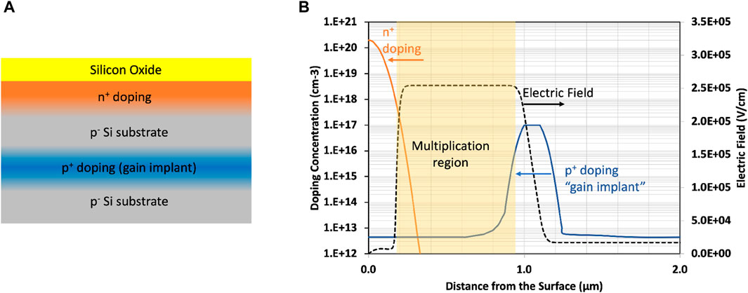
Figure 1. Schematic cross-section of the LGAD multiplication junction (A) and representation of the doping profiles and electric field as a function of the depth (B). The plotted values are only representative of the technology and do not refer to any specific device.
The region with the high electric field, where the impact ionization happens, is indicated as “multiplication region” or “gain layer”. The doping profiles of the multiplying junction are typically fabricated using ion implantation, even if other approaches, such as dopant diffusion by solid or gaseous sources and doping during epitaxial growth, are possible. The Boron doping profile typically peaks at 1–1.5 μm for the front surface, resulting in a multiplication region extending from a few hundred nanometers from the surface up to the falling edge of the Boron implant at about 1.5–2 μm. A review of LGADs fabrication technologies is available in [21].
The first prototypes of LGADs were manufactured by the Centro Nacional de Microelectronica (IMB-CNM, Barcelona, Spain) in 2013 [16]. Since then, the technology has undergone further developments and has reached a good technology readiness level within the CERN RD50 collaboration1. Currently, many research facilities around the world are involved in LGAD manufacturing and R&D, such as: Fondazione Bruno Kessler (FBK, Trento, Italy), Brookhaven National Laboratory (BNL, Upton, United States) IMB-CNM, Hamamatsu (Japan), IHEP-NDL (Beijng, China), USTC-IME (China), Micron (Lancing, United Kingdom), Teledyne e2v (Chelmsford, United Kingdom), SINTEF MiNaLab (Oslo, Norway).
The first LGADs were manufactured on approximately 300 μm thick p-type Float-zone (FZ) wafers by IMB-CNM and FBK [16, 22]. The early devices showcased the potential for signal multiplication of around 10 but the temporal resolution remained constrained, typically in the range of 100 ps. To further improve the time resolution in MIP detection, a new generation of LGADs was then produced on thinner substrates of 45–60 μm [23–25].
The advantage of using thin substrates originates from the peculiar shape of the signal generated by a MIP in LGADs: it has a rise time that is as long as the drift time of an electron traversing the entire sensor thickness. Therefore thinner substrates originate signal waveforms with a higher steepness. A detailed discussion of the signal shape for an LGAD is reported in [15]. Considering the voltage waveform after the amplifier stage, the signal steepness or “slew-rate” is indicated as
where d is the depleted (or “active”) sensor thickness and G represents the gain. This equation is only valid under the assumption of a uniform charge generation throughout the sensor thickness, and considering an ideal pad geometry (neglecting the border effects). Reducing the sensor’s active thickness improves the slew-rate but increases the junction capacitance, negatively affecting the time resolution. The optimal balance between these factors depends on the specific application and the readout electronics being used.
A similar trade-off can be found for the gain: a high gain value increases the signal slew-rate but a too high gain is detrimental to the SNR, due to higher shot noise. In addition, increasing the sensor gain by adjusting the operating voltage also results in increased current and bias voltage, leading to higher power consumption. An alternative approach is to increase the doping level of the gain implant, which allows for high gain at lower bias voltage, thereby limiting power consumption. However, this solution may not always be practical as it could prevent the electron velocity from saturating throughout the entire depleted volume, which can be detrimental to time resolution [15]. In HEP timing applications, experimental results and simulations indicate that a thickness of
In a silicon processing clean room,
2.1.1 LGAD segmentation
The initial strategy for creating segmented LGADs adopted the same segmentation scheme employed in standard n-i-p diode arrays. This approach entails the segmentation of the entire n+-p−-p+-p− multiplying junction, with the addition of an extra p-type region referred to as a “p-stop” between the pixels to ensure full electrical isolation, as illustrated in Figure 2. However, the segmentation of a sensor with internal multiplication presents additional challenges compared to conventional p-i-n diodes. Indeed, to avoid undesired high-electric field regions at the termination edge of the gain layer, an additional n-type region known as Junction Termination Extension (JTE) is typically included. The JTE controls the n+ curvature and reduces the electric field at the pixel border. The gain layer is removed in the JTE and p-stop regions and also indented from the JTE edge to prevent premature breakdown at the pixel edge (edge-breakdown). These termination structures use some of the sensor’s area and, as a consequence, introduce an inter-pixel region where the gain is suppressed [26]. This is the so-called no-gain region, defined as the distance between two adjacent gain implant regions. In standard LGADs, the no-gain region is typically in the range 50–100 μm, depending on the fabrication technology and device design. The presence of such a no-gain region reduces the fill factor (FF) of the pixel (FF = pixel area with signal multiplication/total pixel area).
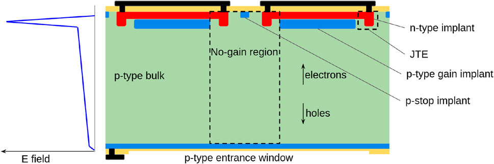
Figure 2. Schematic cross-section of a standard LGAD and magnitude of the electric field inside the sensor. Yellow represents dielectrics and black the metallization. The readout side is on top, and the x-rays enter from the bottom. The entrance window was added for the application of these sensors to x-ray detection.
In current HEP experiments, where the required pixel size is typically around 1 mm2, the FF loss is almost negligible. However, in photon science applications, where a pixel size in the range of 25–100 μm is usually required, the wide inter-pixel region makes the standard LGAD technology inadequate.
2.2 Capacitively coupled LGAD (AC-LGAD)
The first technological solution proposed to overcome the segmentation issues in LGADs was the capacitively coupled LGAD (AC-LGAD) [27, 28]. In this architecture, the multiplying junction (both n+ and p+ layers) is not patterned and covers the full sensor area, without any interruption. The read-out is kept on the same side of the multiplication region and the sensor segmentation is achieved via metal pads AC-coupled to the n+ layer via a thin dielectric film (about 100 nm thick). The n+ layer is then connected to the ground at the sensor periphery, where the JTE is present as in the case of standard LGAD. A sketch is shown in Figure 3. In this scheme, thanks to the uniform multiplication region across the sensor, a 100% fill factor is achieved with uniform multiplication and no dead areas, independently of the channel segmentation.
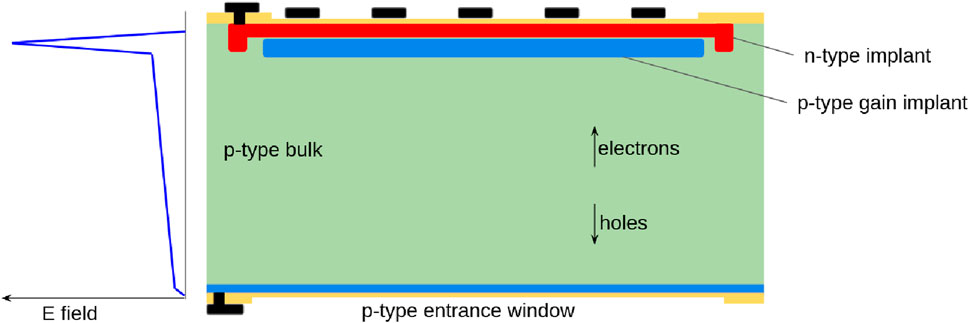
Figure 3. Schematic cross-section of an AC coupled LGAD and magnitude of the electric field inside the sensor. Yellow represents dielectrics and black the metallization. The readout side is on top, and the x-rays enter from the bottom. The entrance window was added for the application of these sensors to x-ray detection.
Signal formation in an AC-LGAD differs significantly from the one of a standard LGAD [29]. In AC-LGADs, the signal at the readout pads is primarily induced during the charge propagation along the n+ layer, before discharging to the ground. The resulting signal is bipolar, with a zero net integral. The positive lobe is generated during the current lateral spread along the lossy transmission line composed of the n+ layer, the bulk, and the AC-pads. The negative lobe accounts for the AC-pad discharge, with an RC constant that depends on the read-out input resistance, the n+ sheet resistance and its capacitances towards the sensor backside and the metal pads.
In AC-LGADs, the signal could propagate in the n+ layer for hundreds of microns before being completely collected by the pick-up electrodes, as a consequence, a certain amount of cross-talk exists among adjacent pixels. Signal-sharing among pixels can be used to enhance spatial resolution by interpolating signals from neighboring pixels. This resistive read-out method was first investigated by INFN and the University of Turin for AC-LGADs, which they called Resistive Silicon Detectors (RSD) [28]. They demonstrated that RSDs can detect MIPs with a similar temporal resolution of standard LGADs (approximately
AC-LGAD detectors have been manufactured by various research facilities, primarily on thin epitaxial silicon substrates (approximately 50 μm) for HEP tracking. However, a prototype on a thick FZ silicon substrate was presented in [22]. If produced on thick FZ silicon wafers using a double-sided manufacturing process (see Figure 3) this device becomes capable of detecting photons and particles entering from the sensor backside. Here, a p+ implant and a thin passivation layer can be implemented, forming an entrance window.
Despite the promising attributes, such as fine segmentation and a 100% fill factor, which make AC-LGADs appealing for photon science applications, their use in this field is now hampered by the peculiar shape of the produced signals: the fast and bipolar signals are not compatible with charge-integrating electronics or with the current single-photon counting front-end used in photon science, as the long integration time would produce zero-net-charge signals. Some authors suggested that this effect can be attenuated in single-photon counting detectors by making the n+ layer float through a large value resistor connected between ground and the n+ contact [27]. Electrons collected at the n+ layer will then discharge with a long time constant, producing a signal with negligible opposite polarity pulse amplitude. In conclusion, to fully exploit this technology in photon science applications, significant modifications of the read-out electronics or optimization of the sensor output are required.
2.3 DC-coupled resistive silicon detectors (DC-RSD)
A further development, exploiting the resistive readout employed in AC-LGADs led to the proposal of DC-coupled resistive silicon detectors (DC-RSD) by INFN and the University of Turin [31]. Similar to AC-LGADs, the multiplying junction in DC-RSD is not patterned and extends to the entire sensor area. However, in DC-RSD, the metal pads are directly connected to the n+ layer via ohmic contacts (refer to Figure 4). Electrical isolation among different channels is achieved by designing an n+ layer with sufficiently high sheet resistance and optimizing the inter-pads distance accordingly. The motivation behind the development of DC-RSD lies in two main objectives: 1) restricting the spread of signals beyond the nearest pads to enhance spatial resolution, and 2) generating unipolar signals instead of the bipolar signals produced by AC-LGADs. DC-RSD can be also produced using a double-sided process, allowing for the incorporation of an entrance window on the backside for applications involving photon and x-ray imaging. While this technology promises to address some of the limitations associated with AC-LGADs, its development is still ongoing, and experimental validation is still needed.
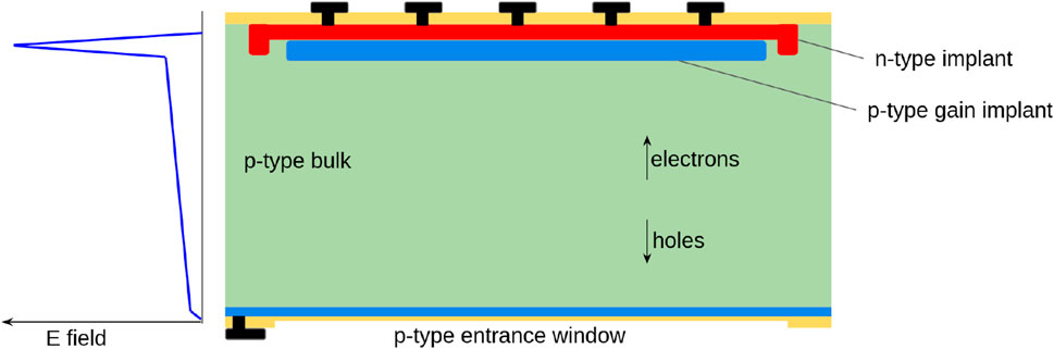
Figure 4. Schematic cross-section of DC-RSD and magnitude of the electric field inside the sensor. Yellow represents dielectrics and black the metallization. The readout side is on top, and the x-rays enter from the bottom. The entrance window was added for the application of these sensors to x-ray detection.
2.4 Inverted LGAD (iLGAD)
An alternative approach aimed at achieving high spatial resolution using a structure based on LGADs is known as the inverted LGAD (iLGAD) [32]. Originally proposed in [33] and previously referred to as double-sided LGADs, this design features a multiplication junction formed by a uniquely unpatterned region covering the entire sensor, ensuring a 100% fill factor, while the read-out segmentation is provided by the collecting electrodes on the opposite side (ohmic or read-out side), without compromising the gain uniformity along the sensor (refer to Figure 5).
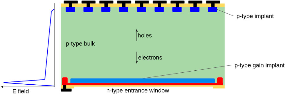
Figure 5. Schematic cross-section of a double-sided (inverted) LGAD and magnitude of the electric field inside the sensor. Yellow represents dielectrics and black the metallization. The readout side is on top, and the x-rays enter from the bottom. Figure originally published in [34].
To ensure full electrical isolation among the read-out channels, the device must operate in full depletion. Additionally, as a full double-sided process is required to define both surfaces of the wafer, the latter must be approximately 200–300 μm thick. Unfortunately, such a high active thickness compromises the timing capability of iLGAD (see Eq. 1), making this technology less appealing in HEP applications where fast timing is crucial. However, due to its exceptional segmentation capabilities, iLGAD is valuable for applications where the timing information is not critical. It stands out as the predominant LGAD technology for these applications, as discussed in Section 3.
2.4.1 n-type iLGAD
In iLGADs, the integration of the read-out on the opposite side of the sensor necessitates placing the entrance window for photons and x-rays on the gain side. This feature introduces a dependence of the multiplication on the particle interaction point. In p-type LGADs, the multiplication process for low-energy particles, interacting close to the surface (in the superficial neutral region) is initiated by holes traveling through the gain layer. For particles interacting deeper in the substrate, the multiplication is electron-initiated. The latter process produces signals with both higher gain and SNR, as discussed in Section 5.
To address this limitation and enhance the efficiency of detecting low-energy photons and particles, iLGADs on n-type substrates have also been proposed in [35], and experimentally fabricated by IMB-CNM [36]. This sensor was named proton Low Gain Avalanche Detectors (pLGAD) and features inverted doping compared to traditional iLGAD (as represented in Figure 6). Such a sensor was also provided with a thin surface passivation layer and an entrance window optimized for the detection of particles with a low penetrating depth (15 keV protons in this specific case, which have a maximum range in silicon of 300 nm). In such a detector, only signals created close to the entrance window are amplified with high gain (a gain of around 18 was reported). A new advancement in fabricating n-type i-LGADs for soft x-ray detection was also recently presented at a conference [37]. The work reported on the first LGAD prototypes equipped with a thin entrance window for photons with energy as low as 250 eV. The initial characterization showed a gain of about 7 when illuminated with 470 nm light, that corresponds to an attenuation length of 0.56 μm in Silicon. The gain drops to 1.4 when illuminated with 940 nm photons, which interact deeper in the substrate (attenuation length equal to 54.6 μm) and generate hole-initiated multiplications.
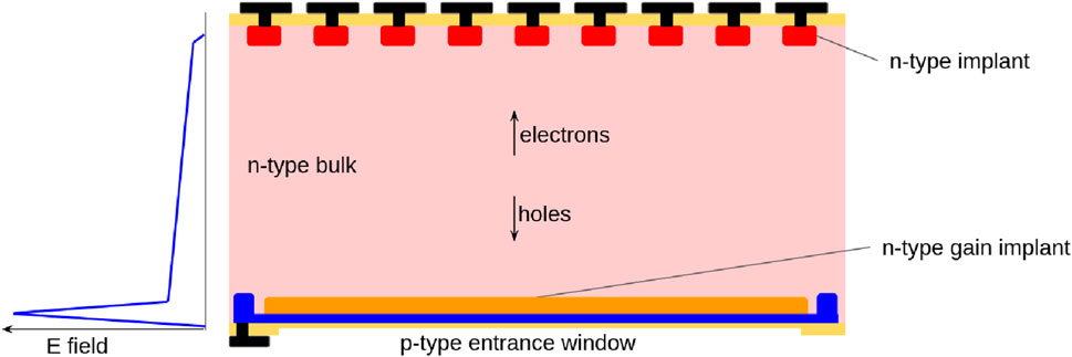
Figure 6. Schematic cross-section of a n-bulk inverted LGAD and magnitude of the electric field inside the sensor. Yellow represents dielectrics and black the metallization. The readout side is on top, and the x-rays enter from the bottom.
The mentioned results make the n-type i-LGAD unfit for HEP applications but perfectly suited for low-energy physics experiments.
2.5 Trench-isolated LGAD (TI-LGAD)
An alternative technological approach to achieve fine segmentation in LGADs involves the use of narrow and shallow trenches to isolate the pixels, as represented in Figure 7. This technology is based on etching a pattern of trenches into the silicon substrate, which are then filled with dielectric materials, such as silicon dioxide. The trenches, approximately 1 μm wide, replace all the structures at the pixel border region, such as p-stop and JTE, while maintaining the same multiplying junction scheme (n+-p−-p+-p−) as standard LGADs. This design offers a clear advantage in terms of reducing the no-gain width between adjacent pixels, overcoming the technological limitations of the standard approach.
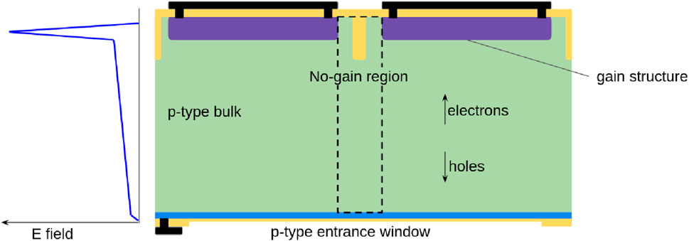
Figure 7. Schematic cross-section of a trench isolated LGAD and magnitude of the electric field inside the sensor. Yellow represents dielectrics and black the metallization. The readout side is on top, and the x-rays enter from the bottom. The entrance window was added for the application of these sensors to x-rays detection.
Thanks to the trench isolation technology, the nominal no-gain width can be reduced to less than 5 μm, compared to the usual few tens of microns in standard LGADs, achieving an outstanding 80% fill factor for a 50 μm pitch sensor. TI-LGADs were proposed and initially produced by FBK based on thin epitaxial wafers [26], with a first characterization reporting an effective no-gain distance between pixels as low as 2 μm [38].
TI-LGAD sensors manufactured with a double-sided process hold promise for soft x-rays detection. They can provide a reasonably high fill factor, small pixels down to 25 μm, and simultaneously offer the possibility to integrate an entrance window on the sensor backside. As of now, no experimental prototypes made on FZ thick substrates are available. Additionally, using a thicker active layer (e.g., 300 μm) necessary for a fully double-sided process could potentially be detrimental to the no-gain width. This effect is attributed to the peculiar shape of the electric field at the pixel periphery, as discussed in [26].
2.6 Deep-junction LGAD (DJ-LGAD)
Another promising LGAD technology, the deep-junction LGAD (DJ-LGAD), has been introduced and pioneered by the University of California, Santa Cruz [39]. A cross-sectional representation of the device is depicted in Figure 8. In this design, the multiplying junction forms a uniform area of n+ and p+ gain implants spanning the entire sensor area. Unlike other LGAD technologies, the multiplying junction is not superficial but is buried a few microns below the surface, where n+ DC-coupled electrodes are positioned.
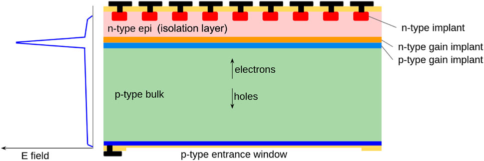
Figure 8. Schematic cross-section of a deep junction LGAD and magnitude of the electric field inside the sensor. Yellow represents dielectrics and black the metallization. The readout side is on top, and the x-rays enter from the bottom. The entrance window was added for the application of these sensors to x-rays detection.
The bulk of the sensor comprises high-resistivity p-type silicon, and above the buried junction, a several-micron-thick layer of high-resistivity n-type material, referred to as the “isolation layer,” is present. At the operational bias voltage, both the n-type epi and p-type bulk regions are depleted. However, the multiplication region is confined between the buried n+ and p+ gain layers while elsewhere the electric fields are well below the threshold for impact ionization. The lateral termination of the multiplication structure can be realized by extending the n+ gain layer to be close to a grounded guard ring while the p+ gain layer is a few μm narrower than the n+ layer, as suggested in [39]. Below the junction, the thicker layer of high-resistivity p-type material serves as the charge generation medium for detecting charged particles, x-rays, or heavy ions. An optical window can be included on the p-type side of the sensor, along with the back bias electrode.
Particles interacting in the n-type isolation layer undergo holes-initiated multiplication and do not experience significant multiplication. Conversely, electrons drifting from the p-type bulk are multiplied in the gain layer and then drifted to be collected by the n+ electrodes at the top surface. Proper tuning of the n− and p-type regions allows for optimization of both noise and energy sensitivity for specific applications.
The unique design of this detector introduces some fabrication complexity and new challenges, primarily due to the necessity to manufacture the buried junction several microns into the substrate. One approach involves using a substrate with the two n- and p-type high-resistivity regions, obtained, for example, through a double epitaxy process or wafer-to-wafer direct bonding. High-energy ion implantation is then employed to place the two gain doping profiles at the n-p interface. However, this technique has intrinsic limitations due to the maximum achievable energy of standard ion-implantation equipment (a few MeV), restricting the junction depth to 4–5 microns from the sensor surface.
An alternative method involves implanting the two gain layers on two different wafers, which are then wafer-bonded together. The wafer carrying the n+ gain layer is subsequently thinned down to a few microns, and its surface is processed to allocate the electrode structures. Another approach includes using a p-type substrate where both the two gain implants are done close to the surface, followed by the growth of the high-resistivity n-type layer by epitaxy.
Several institutes and research facilities are conducting R&D activities to produce first prototypes of DJ-LGADs, but preliminary results are not yet published, with only partial results presented in workshops [40].
3 Review of recent results from LGADs for X-ray detection
In the past few years LGAD sensors were tested as x-ray detectors, this section summarizes the results obtained in these studies proceeding in chronological order.
The very first measurements showed that LGAD sensors could be used as x-ray detectors using standard LGADs with a pad geometry of 5 × 5 mm2 and a thickness of 200 μm. These sensors demonstrated the detection of x-rays down to the energy of Mo fluorescence (17.5 keV), with the lowest detectable energy being limited by the sensor capacitance [19].
The first tests with tender x-rays were done using standard LGADs developed for high energy physics, featuring an active thickness around 50 μm and a low resistivity substrate with a thickness in the order of 500 μm. The low resistivity substrate does not allow for a backside illumination of the sensors with soft x-rays, making it favourable to test them with the x-rays impinging on the front side of the sensors where a few μm of dielectrics and metal are usually present. Using a bunched x-ray beam with a repetition rate of 500 MHz, the detection of 6 keV photons was demonstrated using a sensor with pad geometry of
Standard LGAD 5 mm long strip sensors with a pitch of 150 μm and active thickness of 50 μm were connected to both charge integrating [41, 42] and photon counting [43] readout electronics. The larger channel capacitance of the LGAD sensor (due to its strip geometry and thickness) compared to a standard silicon sensor resulted in increased noise and is detrimental to the energy resolution. Despite this effect, photons with energy of 2.1 keV were detected with the photon counting electronics, showing an improvement with respect to the 8.5 keV energy threshold achieved with a standard silicon sensor with the same electronics settings [44]. The energy resolution using the photon counting electronics was 0.31 keV for 2.1 keV x-rays, and the charge integrating electronics showed a resolution of 0.41 keV for 8.05 keV x-rays, with the latter figure representing a factor 2.7 improvement compared with a standard silicon strip sensor read out by the same charge integrating electronics [44]. The ASICs combined with a standard LGAD strip sensor resulted also in an improved energy resolution compared to the previous result obtained with standard LGADs read out using discrete component electronics. A dependence of the energy resolution on the x-ray energy is observed also in this study. Furthermore it is shown that there is an optimal operating voltage that gives the best resolution due to the rise of shot noise when further increasing the gain of the LGAD sensor [44]. The noise of the readout system when expressed in x-ray energy (keV equivalent) is shown to decrease with the LGAD operating voltage. This is due to the sensor gain that changes the conversion between collected charge and x-ray energy [44]. The results shown in [44] also highlight two main drawbacks of standard LGADs optimized for timing: the aforementioned channel capacitance with typical values around 3 pF) and the fill factor of these sensors that strongly limit their use in synchrotron radiation applications. The use of iLGADs can improve both aspects, lowering the channel capacitance and providing a 100% fill factor. A thin entrance window applied to these sensors would then allow for an improved quantum efficiency for soft x-rays.
These sensors were fabricated and considerations for their design, together with a first characterization, are shown in [45]. A 1 × 1 cm2 iLGAD pixel sensor with 25 μm pitch and 275 μm thickness was bonded to a charge integrating readout electronics [10]. The sensor leakage current and its noise were improved by cooling the sensor-ASIC assembly, resulting also in an increase of the sensor’s gain [45].
Due to x-ray interactions, the use of iLGADs for synchrotron light applications causes the silicon dioxide to acquire a positive charge, that over time can impact the sensor performance. The effect of this type of radiation damage was explored for iLGADs and a modification of the sensor periphery resulted in an improved radiation hardness for x-rays [46].
The characterization of standard LGADs continues in parallel to iLGAD development. Standard LGAD pad sensors with an area of 1.3 × 1.3 mm2 and thickness of 20 and 50 μm were characterized using a 500 MHz bunched x-ray beam with energy between 5 and 70 keV [47]. The sensors were read out using discrete components electronics. The x-ray bunches could be resolved, maintaining the earlier result of the same group [20]. In this study the timing performance of the sensors was studied more accurately, showing a time resolution between 50 and 200 ps for LGADs and of ∼80 ps for a 50 μm thick silicon sensor with the same pad geometry. The 20 μm thick LGAD performed better than the 50 μm thick ones, with the latter having a time resolution worse than 100 ps. The LGAD timing performance is significantly worse than what is observed for minimum ionizing particles (MIPs), usually around 30 ps. This is explained considering the shape of the deposited ionization cloud in the sensor: a cylinder along the whole sensor thickness for a MIP and a point-like distribution for x-rays. The shape of the ionization cloud together with the signal formation mechanism in LGADs and sensors without gain account for the different performance with the two particle types and the better resolution of a sensor without gain compared to an LGAD of the same thickness [47]. The effect of the different shapes of the ionization cloud for MIPs and x-rays also resulted in a reduction of the sensor gain for the latter [47]. A dependence of the sensor gain on the density of the ionization cloud reaching the gain layer was also studied in the detection of MIPs [48]. Both studies reach the shared conclusion that too high charge density, resulting from the multiplication, can lower the electric field in the gain layer, self-quenching the multiplication process. The energy resolution of the LGADs was studied and found to be between 6% and 20% depending on the bias voltage [47]. The sensors also show a worse resolution at higher operating voltages as shown in [44]. The linearity in the energy response of these LGAD pads was found to be better than 4% [47]. In the same study AC-LGAD strip sensors with a strip length of 5 and 10 mm were exposed to the same x-ray beam and demonstrated an energy resolution between 12% and 21% [47].
The last sensor characterization study to be mentioned in this section features the same 275 μm thick iLGADs used in [45] but with pad geometry. In the study the photocurrent generated by monochromatic x-rays with energies from 200 to 1000 eV was measured. The gain as a function of photon energy of iLGADs was measured, and their quantum efficiency (QE) was estimated using sensors without gain with the same TEW as the iLGADs [49]. The QE measurement of the sensors without gain shows a QE between 55% and 65% for 250 eV photons. Using the dependence of the QE on x-ray energy, the main parameters of the TEW were extracted, showing that the main source of inefficiency are the dielectric layers used on the TEW, while the charge collection efficiency is close to unity [49]. The gain of the iLGAD shows a dependency on the photon energy, with higher gains being achieved at higher energies. This is explained by the distribution of the x-ray interaction positions relative to the multiplication structure [49]. The dependence of gain on x-ray energy is exploited to infer the gain as a function of the position of the x-ray interaction within the sensor. Different multiplication structures were studied, whose multiplication regions were placed at different depths in the sensors. The gain for electrons (holes) entering the multiplication structure Mn (Mp) was determined and it is shown that a thinner multiplication structure has a larger Mp/Mn ratio than a broader one [49]. The effect of the depth of interaction of the x-ray photons relative to the multiplication structure and the ratio between Mn and Mp are discussed in Section 6.
The characterization work done on LGADs using x-rays and the fabrication of sensors dedicated to photon science is a sign of interest in this technology. The performances of the sensors and the level of detail reached in their characterization are steadily evolving. These sensors are close to being employed in measurements at synchrotron light sources instead of being brought to the beamlines to be characterized. The first use of LGAD sensors for photon science measurements is mentioned in a conference [50] and documented in an article preprint [51] where an iLGAD pixel sensor was used in ptychography measurements with soft x-rays.
4 Thin entrance window for soft X-rays
Detecting soft and tender x-rays in the energy range of 200 eV to 2 keV presents new challenges, particularly in achieving high quantum efficiency. In hybrid silicon detectors, x-rays enter the sensors from the side opposite to the collecting junction where the read-out electronics is located. Similarly, in CMOS sensors, the wafer is thinned from the backside to approach the active volume of the sensor. In both cases, an entrance window must be designed and incorporated into the sensor backside to facilitate proper x-ray transmission and the collection of photogenerated charge in the sensor medium. The entrance window comprises two distinct regions: 1) an insensitive layer made of dielectric material or metal, deposited onto the silicon surface, and 2) a highly doped silicon layer (typically of the same sign as the substrate if the entrance window is opposite to the junction).
The QE for soft x-rays interacting closely to the surface may be affected by three loss mechanisms: 1) the absorption of photons in the insensitive layer; 2) the recombination of charge carriers generated by x-rays at the silicon surface, or 3) the loss of charge carriers in the neutral highly doped region via trap-assisted or Auger recombination. In simpler designs, the entrance window is typically made of a thin metal layer (usually aluminum), connected to a highly doped region. However, this design significantly affects QE at low energies due to absorption in the metal and recombination at the silicon-metal interface, where the surface recombination velocity (SRV) approaches the saturation value (approximately 106 cm/s). A more efficient approach involves using a thin layer of dielectric material to passivate the silicon surface and reduce SRV. Materials like thermal silicon dioxide can provide good surface passivation with SRV as low as 10 cm/s. Excellent alternatives are hydrogenated silicon nitride (deposited by Plasma Enhanced Chemical Vapor Deposition - PECVD) [52] and aluminum oxide (deposited using Atomic Layer Deposition - ALD) [53]. Nevertheless, it is crucial to maintain the film thickness as low as possible due to the attenuation length of soft x-rays in the mentioned materials, which is comparable to that of Silicon (Figure 9).
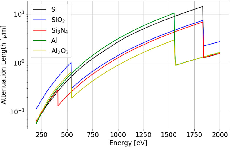
Figure 9. Attenuation length as a function of x-ray energy for Silicon and materials commonly used in the realization of entrance windows for x-rays. Data from [54], that is based on [55].
Manufacturing of thin entrance windows (TEW) for soft x-rays poses challenges due to the strong dependencies of doping concentration profile, surface passivation, and carrier lifetime on specific fabrication processes. While it is difficult to provide a universal set of parameters, a well-passivated silicon surface via a dielectric thin-film coupled to a shallow and steep doping profile with a surface concentration in the order of 1019 atoms/cm3 promises good QE for energies down to 250 eV [56]. Only a few studies systematically investigated TEW for soft x-rays. One recent study investigated the manufacturing of TEW on n-type silicon sensors by using low-energy Arsenic ion implantation or Phosphorous diffusion, and a thin dielectric layer as passivation material. Using LED light they estimated a QE around 50% at 276 eV for wafers fabricated using As ion implantation annealed at high temperatures, and equal to 70% by using Phosphorous diffusion [57]. Another study on back-side illuminated CMOS sensors reported a remarkable QE above 90% in the 100–1000 eV range, corresponding to an equivalent 5 nm dead-layer [58]. This result was obtained on CMOS x-rays sensors back-thinned down to 9.5 μm, and doped with low-energy ion implantation.
As discussed in this paper, the integration of a TEW into LGADs can occur on either the gain side or the bulk side, depending on the specific technology. For AC-LGADs, DC-RSDs, TI-LGADs, and DJ-LGADs, the TEW can be placed on the back side, opposite to the gain, following a similar approach used in standard silicon sensors. For iLGADs, where the TEW is positioned on the multiplication side of the sensors, certain constraints in tuning the doping profile and in the thermal budget have to be considered to preserve the multiplication junction functionality. One of the first studies that investigated the QE on a p-type iLGAD, reported a QE around 60% and 90% at 250 eV and 500 eV, respectively, with charge collection efficiency close to 1 in the full investigated energy range [49]. The encouraging outcomes suggest that incorporating an effective TEW in an iLGAD structure is viable, as the QE appears to be only limited by absorption in the dielectric material, and potential enhancement may be achieved by further reducing the thickness of this insensitive layer. Other studies have successfully demonstrated the integration of a TEW on n-type iLGAD using a 4 nm thick layer of aluminum oxide and 15 nm of aluminum, but no characterization with soft x-rays has been reported [36].
Recent advancements in microfabrication technologies suggested novel techniques for manufacturing TEW for low-energy particles or ultraviolet (UV) light. For instance, using low-energy (5 keV) Arsenic implantations followed by low-temperature (500°C) microwave annealing has been proposed to achieve unitary internal QE at 200 eV [56]. Other advanced techniques, such as plasma immersion ion implantation (PIII) followed by laser annealing, have already proven their effectiveness in detectors for UV light [59]. Compared to conventional ion implantation, PIII can implant at energies below 0.2 keV and when coupled with laser annealing it allows for obtaining a very shallow junction with an abrupt profile, by limiting the dopant diffusion. Alternative technologies to ion implantation have also been proposed: Pure-B deposition has been demonstrated able to produce shallow junctions for UV light detection below 220 nm [60], while superlattice-doping via Molecular Beam Epitaxy (MBE) reached record QE at deep and far UV wavelengths [61].
5 Theory summary of signal and noise of LGAD sensors
This section presents a summary of the theory used to describe the signal and noise properties of the multiplication structure of LGADs. The main references for this section use the local theory of impact ionization developed for avalanche photodiodes [62, 63]. A more accurate description takes into account the space needed by the charge carriers to reach the energy necessary for impact ionization (non-local impact ionization theory) [64, 65]. An example of the considerations presented below applied to APDs for light detection can be found in [66].
The multiplication structure of an LGAD can be represented as shown in Figure 10 where the multiplication of charge carriers happens in a region between 0 and w. In this region the ionization coefficients, denoted as α for electrons and β for holes, are larger than 0. The ionization coefficients are functions of the electric field and therefore of the position in the multiplication region. The currents traversing the system are In and Ip for electrons and holes respectively (the figure reports the direction of motion of the charge carriers). A generation rate g(x) due to thermal effects or particle interaction is considered in the multiplication region. This general representation was used in [62] to derive expressions for gain and noise of avalanche photodiodes. This section summarizes the relevant elements for LGAD sensors. The multiplication factor M(x) is the average total number of electron-hole pairs that are generated in the multiplication region as a result of one initial pair being generated at a position x. The multiplication factor takes the form (Eq. 2)
Neglecting trapping and recombination effects, the multiplication factor varies as a function of x only in the multiplication region, remaining constant outside. For a given electric field, in silicon, β < α [67] resulting in a lower gain for holes entering in the gain region when compared to electrons (M(0) < M(
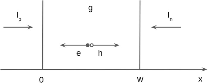
Figure 10. Geometry used in [61] to describe the multiplication region of LGADs. The electric field is high enough to result in multiplication between 0 and w. In the same area a generation rate g due to thermal effects or particle interaction is considered. Ip, In are the holes and electrons currents in the device, respectively. Note that the arrows below the currents Ip, In represent the direction of movement of the respective charge carriers.
Considering the currents Ip(0) and In(
The multiplication affects the noise of the sensor by increasing its leakage current and due to the fluctuations of the multiplication for each charge carrier traversing the multiplication region. This in particular affects the shot noise of the sensor. For a readout bandwidth B, the current fluctuations due to shot noise are
where qe is the elementary charge. In LGAD sensors the width of the multiplication region is smaller than the active thickness of the sensor, representing at most a few percent of it. Assuming that generation effects related to the electric field in the multiplication region (e.g., trap assisted tunneling and field-enhanced emission) do not play a major role, the current generated in the multiplication region can be neglected in comparison to the current generated in the rest of the sensor volume. Disregarding the current generated in the multiplication region (g = 0) the shot noise spectral density can be expressed as
As in silicon Mn > Mp, the holes excess noise factor is larger than the electrons one (Fp > Fn). The excess noise factors do not depend only on the values of gain at the edges of the multiplication structure, but are sensitive to the shape of the electric field in the multiplication region. In the approximation β = kα with k being constant, it is possible to show that the excess noise factors can be reduced if the multiplication of holes is kept at a minimum (k ≪ 1) [62] and it is shown experimentally in [66]. If the gain for holes entering the multiplication region is not important for x-ray detection, reaching a given electrons gain Mn with a broader multiplication region results in lower excess noise factor values.
The shot noise can be expressed in units of electrons using a time constant τ related to the bandwidth of the readout electronics τ = 1/(2B), taking the form
where A3 accounts for the effect of the readout electronics, considering that electronics with the same bandwidth can result in different values of σe depending on their delta-pulse response function [68]. The A3 parameter can assume values between 0.5 and a few units [68], however, for the sake of simplicity, A3 is set to 1 in the rest of this section. τ is also related to the time response of the readout electronics and is usually referred to as shaping time. Using Eq. 6 with A3 = 1, the shot noise becomes (Eq. 7)
where Nn, Np are the number of electrons and holes entering the multiplication region in a time τ, respectively. For an equal current value of electrons and holes entering the multiplication region (Nn = Np), the contribution to the shot noise is larger for the electrons as Mn > Mp, so that
The excess noise factor affects also the signal through its multiplication. An x-ray photon of a given energy creates an average of Nx electron-hole pairs in the sensor, these undergo multiplication resulting in a signal S = NxM, where the value of M depends on the absorption position of the x-ray. The variance of the signal due to the multiplication of its charge carriers is given by [63] as (Eq. 8)
where Fsi is the Fano factor of silicon, and F is the excess noise factor at the absorption position of the x-ray. Eq. 5 shows the excess noise factors to be used if the x-ray interaction results in the injection of electrons or holes at the edges of the multiplication structure. If the x-ray interacts in the multiplication region at a position x, considering a point-like ionization distribution resulting from the interaction, the excess noise factor can be extracted from Eq. 4 similarly as done for Fn, Fp by imposing g = g(x′)δ(x′ − x) (where x′ is the integration variable). The excess noise factor for 0 < x <
By including all noise contributions other than the shot noise (e.g., thermal noise, readout electronics noise, etc.) in a term σ0, the total variance of the signal can be expressed as (Eq. 10)
The quantity
It is interesting to compare the signal-to-noise ratio (SNR) of a sensor with gain to the one of a sensor without gain (M = 1, F = 1). In the case of a sensor with gain, the SNR depends on the absorption position of the x-ray. For an x-ray being absorbed at a position x the SNR takes the form
It is worth noting that the SNR of the sensor without gain is always better than the one with gain in case σ0 = 0, that is if the only noise source is shot noise. In case σ0 > 0, the sensor with gain reduces this term by the square of the gain at the absorption position of the x-ray. As in silicon the gain for electrons entering the multiplication region is higher than for holes (M(
The conclusions that can be drawn by this summary are that, in order to achieve the best SNR, it is convenient to have the x-rays interactions in a position where the resulting electrons enter the multiplication region as they have a larger gain and lower excess noise factor compared to holes. At the same time, to reduce the shot noise, it is convenient that the thermal generation current from the sensor bulk results in holes entering the multiplication region as
6 Technological approaches to LGADs for photon science
LGADs for x-ray detection can be realized in different ways, with different LGAD technologies being detailed in Section 2. In general, the multiplication structure can be placed on either the entrance window side of the sensor, on the segmented readout side, deep (more than a couple of μm) below the sensor surface. This section describes these technological choices and their impact on the performance and manufacturing of the sensors.
6.1 Gain structure on the readout side
In soft and tender x-ray detection, when dealing with a sensor thickness of approximately 200 μm or more, positioning the multiplication structure on the readout side of the sensor and allowing x-rays to enter from the opposite side leads to all x-ray interactions occurring in the bulk. As a result, the charge carriers undergo multiplication with a single average value of gain (M is either Mn or Mp). The polarity of the sensors bulk is usually chosen so that electrons enter the gain layer. This results in a larger value of gain for the charge carriers generated in the bulk, whether they result from an x-ray interaction or thermal generation. This configuration results in a better SNR compared to the choice of having holes from the bulk entering the multiplication region. This can be seen by comparing at the terms under the square root in Eq. 11 for a sensor with gain and imposing M(x) = Mn, F(x) = Fn, Np = 0 for the case of a p-type bulk and M(x) = Mp, F(x) = Fp, Nn = 0 for an n-type bulk, with the same generation current so that Nn, Np assume the same value when they are not 0. As the charge carriers entering from the readout side are considered to be negligible compared to the ones coming from the bulk Nn, Np can be set to 0 depending on the bulk polarity. If electrons from the bulk are multiplied, the realization of a given gain would favour a multiplication structure as broad as possible while maintaining a bulk thick enough to absorb the x-rays. This reduces the electric field in the multiplication region and in turn the multiplication of holes, resulting in a reduction of the excess noise factors and an improved SNR.
Placing the multiplication structure on the readout side poses the challenge of the segmentation of the gain layer in order to achieve channel segmentation. This can result in volumes in the sensor where the charge carriers from an x-ray interaction do not undergo charge multiplication. This is the case for standard and trench isolated LGADS. In the case of standard LGADs, the segmentation of the gain layer is not suitable for reaching the pitch needed by pixel or strip detectors for synchrotron radiation experiments as their fill factor would be too poor. Trench isolated LGADs might fulfill the requirements, however their performance regarding the fill factor is not yet demonstrated on substrates of a suitable thickness. The resistivity of the most superficial doped layer of the multiplication region are exploited by AC coupled LGADs and the proposed DC-RSD to achieve channel segmentation without interrupting the gain layer. These sensors feature a continuous gain structure for the whole active area, avoiding regions where the charge carriers from x-ray interactions do not undergo multiplication.
Placing the multiplication structure close to the sensors surface allows to use dopant diffusion or ion implantation to realize the sensors, without the necessity of less common fabrication techniques. A further advantage of this approach is that the TEW can be developed and fabricated almost independently from the multiplication region allowing for an optimization of these components with less constraints.
6.2 Gain structure on entrance window side
Placing the multiplication structure on the entrance window side of the sensor allows to achieve channel segmentation while avoiding to interrupt the multiplication structure. This avoids regions where the charge carriers from x-ray interactions do not reach the multiplication region. Inverted LGADs follow this design, and these are the only LGAD sensor type so far specifically developed for soft and tender x-ray detection [45]. With an absorption length spanning between
In the top row of Figure 11 the multiplication structures are applied to an iLGAD with p-type bulk (see Figure 5). The red line represents M(x) and is referred to the left vertical scale, and the shaded area represents the high field region. Given the polarity of the bulk, the x-ray interactions taking place to the right of the multiplication structure result in electrons entering the high field region. The two colored lines represent the intensity of x-rays of two different energies (350 and 700 eV) and are referred to the vertical scale on the right. The entrance window is placed to the left of the multiplication structure, with the silicon starting at 0 and the bulk extending for
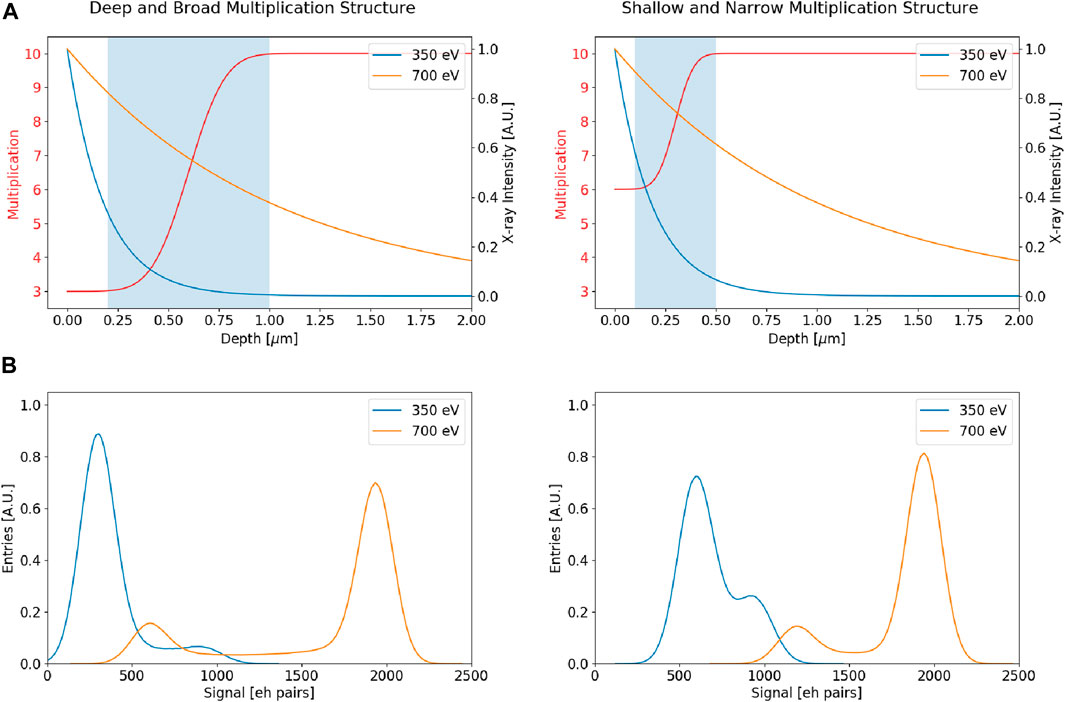
Figure 11. (A) Multiplication and x-ray intensity as a function of depth in silicon for iLGAD sensors. (Left) Deeper and broader gain region. (Right) Shallower and narrower gain region. The shaded area represents the high field region of the sensor. The intensity of 350 and 700 eV x-rays as a function of depth is also shown, and is referred to the right vertical scale. (B) The resulting signal spectra for 350 and 700 eV x-rays. The signal is convoluted with a 100 e− noise.
It is interesting to see the effect of applying the multiplication structures described above to a n-bulk iLGAD sensor (see Figure 6). The results can be seen in Figure 12, where the same quantities as Figure 11 are shown, with the difference that the bulk to the right of the multiplication structure is n-type, resulting in the holes from the bulk entering the multiplication region. The only effect of the change in bulk polarity for this example is which side of the multiplication region reaches a gain Mn or Mp. The areas of the spectra in Figure 12 are the same as in Figure 11, allowing for a direct comparison. The spectrum of 350 eV x-rays for the deep and broad multiplication structure (bottom left of Figure 12) is now dominated by events with Mn gain, while the 700 eV x-rays spectrum is similar to the one calculated for the same multiplication structure and p-bulk iLGAD. The shallow and narrow gain structure on a n-bulk iLGAD results in the spectra in the bottom right plot of Figure 12. For this structure the 700 eV x-ray spectrum is narrower, mainly as a result of the higher Mp of this structure. The 350 eV x-ray spectrum sees a reduction of the peak of events with Mn gain as the multiplication structure is closer to the silicon surface. In the case of the n-bulk iLGAD the deeper multiplication structure shows a better performance than the shallower one. Compared to the p-bulk iLGAD, the n-bulk iLGAD is a more suitable sensor for the lower energies of soft x-rays, while the p-bulk iLGAD performs better with higher energy x-rays. To better see the effect, Figure 13 shows the fraction of interactions resulting in Mp or Mn gain for a n-bulk iLGAD with a deep and broad multiplication structure and the same quantities for a p-bulk iLGAD with the narrow and shallow structure.The n-bulk iLGAD provides a gain of Mn predominantly to lower energy x-rays compared to the p-bulk iLGAD. However, if the gain for holes entering the multiplication structure is high enough, the SNR for the higher energy x-rays might be sufficient for detection as they create a larger number of charge carriers in their interaction with the silicon bulk. The n-bulk iLGAD, for low energy x-rays, can fulfill the conditions derived from the theory of multiplication: a signal where the electrons enter the gain region and noise dominated by holes entering the gain region.
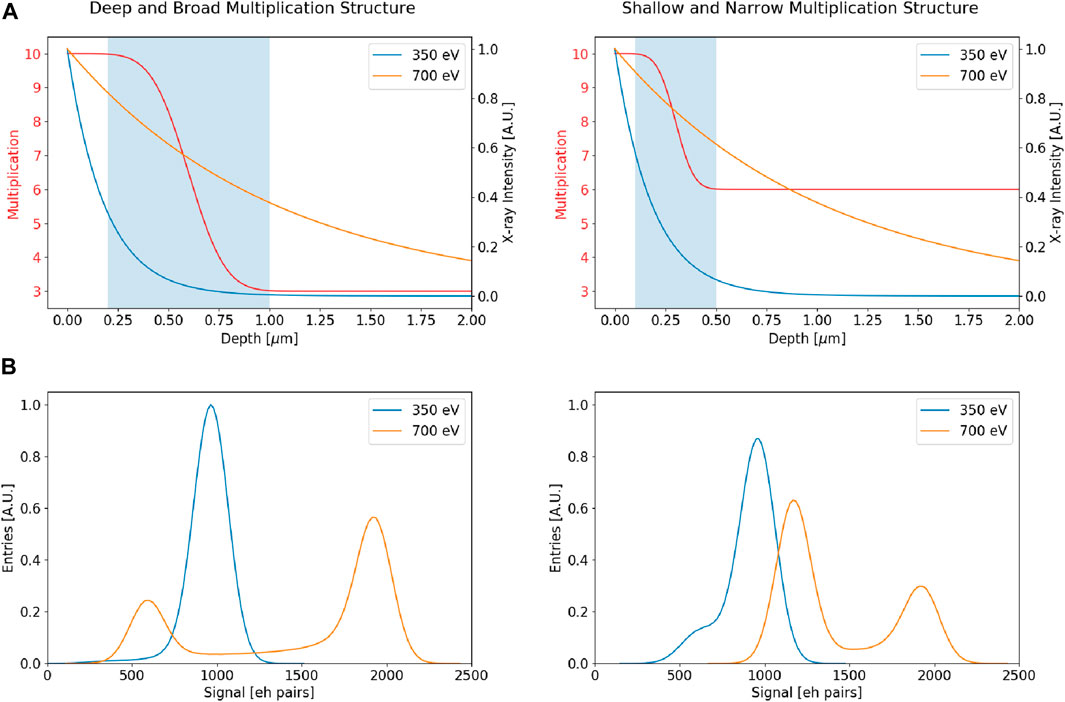
Figure 12. (A) Multiplication and x-ray intensity as a function of depth in silicon for n-bulk iLGAD sensors. (Left) Deeper and broader gain region. (Right) Shallower and narrower gain region. The shaded area represents the high field region of the sensor. The intensity of 350 and 700 eV x-rays as a function of depth is also shown, and is referred to the right vertical scale. (B) The resulting signal spectra for 350 and 700 eV x-rays. The signal is convoluted with a 100 e− noise.
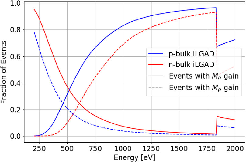
Figure 13. Fraction of events that results in the electrons (full lines) or holes (dashed lines) entering the multiplication region as a function of the x-ray energy. The iLGAD refers to the shallow and narrow multiplication structure shown in Figure 11 top right. The n-bulk iLGAD refers to the deep and broad multiplication structure shown in Figure 12 top left.
Placing the gain structure on the entrance window side of the sensor is the only strategy used so far for LGAD sensors dedicated to photon science applications, with the available sensors having a p-type bulk. N-bulk iLGADs were fabricated with the aim of detecting low-energy charged particles and have not yet been characterized using x-rays. The choice of the bulk polarity allows to choose which energy region receives the higher gain values. As a drawback, these sensors will produce a spectrum with two peaks for most x-ray energies, complicating the interpretation of measurements acquired with charge integrating or spectrally-discriminating ASICs.
Regarding the fabrication of these sensors, their complexity is increased with respect to sensors with the gain structure on the readout side. Both sides of the sensor require the realization of complex structures to allow for a fine-enough segmentation on the readout side and the gain structure coupled with the TEW on the opposite side. As the gain structure is close to the TEW, the optimization of these two components is entangled. Despite their complexity, common fabrication techniques can be used to realize these sensors as their components are placed close to the sensor surfaces.
6.3 Deep gain structure
Placing the gain structure a few μm or further from the readout side of the sensor allows for a continuous structure and a fine segmentation of the readout channels without areas where the charge carriers from the x-ray interactions do not receive multiplication. If the gain structure is close to the readout side, almost all of the soft and tender x-ray interactions will result in electrons entering the multiplication region. A multiplication structure placed a few μm from entrance window of the sensor would result in part of the events where the holes enter the multiplication region receiving a lower gain. This is similar to the situation detailed in the previous sub section. The distance of the multiplication structure from the entrance window of the sensor determines which is the fraction of events resulting receiving Mn or Mp gain. This is shown in Figure 14 for a 1 μm wide gain region placed at different depths in the sensor.
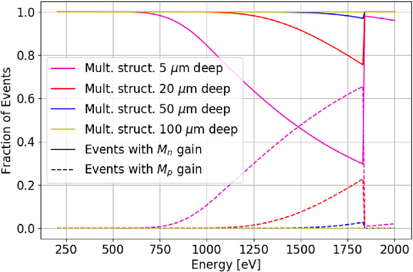
Figure 14. Fraction of events that results in the electrons (full lines) or holes (dashed lines) entering the multiplication region as a function of the x-ray energy. For DJ-LGADs with their multiplication structure at different depths (measured from the entrance window) in silicon.
The dark current in a sensor with a deep gain structure results in both holes (from the n-type region) and electrons (from the p-type bulk) entering the multiplication region. Assuming the same generation rate for both the p- and n-type regions, placing the multiplication structure closer to the readout side increases the fraction of electrons from the dark current entering the multiplication region, and results in a higher noise compared to the same multiplication structure placed closer to the entrance window side of the sensor.
As the fraction of events receiving Mn gain favours a gain structure closer to the readout side and the noise favours a multiplication structure closer to the entrance window, an optimization of the position of the multiplication region is possible if a particular energy of x-rays is targeted for detection.
The realization of a deep gain structure requires methods not often employed in sensor fabrication. In case the structure is placed a few μm from one of the sensor surfaces, high energy ion implantation or epitaxial growth of silicon can be used. In the case of deeper structure, this can be realized through wafer-to-wafer bonding and eventual thinning of one of the starting wafers to achieve the desired position in the sensor. The wafer bonding and epitaxy procedures result in different silicon substrates being placed on either side of the multiplication structure, this can influence the optimization discussed above as the substrates can have different dark current generation rates.
7 Comparison of possible sensor structures
In this section different LGAD technologies are compared in their possible application in photon science. For this comparison it is assumed that all the sensor technologies are produced on thick-enough substrates and are equipped with a thin entrance window for soft x-rays. A few figures of merit are summarized in Table 1 and described below.
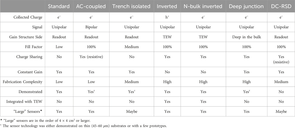
Table 1. Comparison of different LGAD technologies for their application in photon science.
7.1 Collected charge
The sign of collected charge might constraint the ASIC that can be connected to the sensor as some ASICs are optimized for either electrons or hole collection.
7.2 Signal
The sensor signal can either be uni- or bi-polar, the only sensor type with bipolar signals is the AC-LGAD. The AC-coupling of the channels renders impossible the use of these sensors with charge integrating electronics. The readout of AC-LGADs using photon counting ASICs is constraint by the time scale of the development of the bipolar signal: if the signals present both its positive and negative lobe within the integration time constant of the ASIC amplifier, then the signal registered by the electronics might be too small to cross the set threshold. These considerations might render AC-LGADs incompatible with the available ASICs developed for photon science.
7.3 Gain structure side
The side where the gain structure is placed, together with the sensor polarity, has interesting implications for the signals produced by the sensors, as shown in Section 6.
7.4 Fill factor
The fill factor of the sensors is qualitatively categorized. The standard LGAD technology does not allow for the channel segmentation necessary for photon science applications, while TI-LGADs might achieve a sufficient fill factor assuming that the performances obtained on
7.5 Charge sharing
The charge sharing is classified in a qualitative manner. Standard LGADs and TI-LGADs sensors often do not offer this feature that is used to improve the position resolution of the sensors through interpolation. The other considered technologies feature charge sharing, with the AC-LGADs and DC-RSD having a resistive sharing mechanism instead of a charge sharing driven by charge carrier diffusion.
7.6 Constant gain
The constant gain refers to the sensors response to monochromatic x-rays, as discussed in Section 6 the point of interaction of the x-ray photons can impact the gain for each event. All sensor technologies are expected to provide a constant gain for soft and tender x-rays with the exception of iLGADs and n-bulk iLGADs.
7.7 Fabrication complexity
The fabrication complexity qualitatively ranks the sensor technologies. All LGAD sensors are going to have a more complex fabrication process than standard silicon sensors due to the gain implant and the gain termination structure (junction termination extension). The fabrication complexity can have consequences on the cost of the sensors and their yield. Due to the presence of a thin entrance window all sensors require a double sided fabrication process with lithography operations performed on both sides of the silicon wafer. For sake of comparison, the standard and AC-coupled LGADs are assigned a “low” complexity as they present, in principle, the easiest production path. The TI-LGADs together with DC-RSD are assigned a “medium” complexity as the former require the etching and filling of trenches in the silicon, and the latter (yet to be produced) seem to require a precise control of the resistance between channels. The iLGADs of both bulk polarities and the DJ-LGADs are ranked with a “high” fabrication complexity. The iLGADs foresee complex structures on both sensor sides, with the realization of the TEW being entangled with the multiplication structure. The DJ-LGADs require fabrication processes that are not usually employed in standard silicon sensors in order to place the multiplication structure at a depth of more than a couple of μm in the sensor bulk.
7.8 Demonstrated
All sensor technologies considered in the paper have been demonstrated with sensors either produced for high energy physics or photon science, with the exception of DC-RSD that have not yet been produced. The AC-coupled and TI-LGADs were produced so far on thin (45–60 μm) substrates and their performance is yet to be characterized on thicker substrates. Only a few DJ-LGAD sensors have been produced, so this technology is not considered to be at the same level as others.
7.9 Integrated with TEW
For soft and tender x-ray detection the integration of a TEW with the sensor is necessary. So far only iLGADs of both bulk polarity have been produced with an integrated TEW.
7.10 “Large” sensors
The last figure of merit is the possibility to produce “large” sensors, with a dimension of about 4 × 4 cm2 or larger. The possibility of covering a sufficient area is fundamental in order to obtain all the necessary data from measurements at synchrotron light sources, providing a large enough acceptance without gaps in the sensitive surface of the sensors. The distance between the sample being studied and the sensor is also important in order to exploit the “lever arm” so that the relevant features projected on the sensor appear far enough from each other to be resolved by the sensor. In this context a sensor with a too-small area will need to be placed either too close to the sample for this separation to be present or will not cover enough of the solid angle to collect all the needed information. In this section, the considered limit in realizing large sensors is given by the lithographic technology necessary to realize the sensors. TI-LGADs require the fabrication of trenches with a width of less than 1 μm, a feature size that is only possible with projection lithography. This lithography technique allows to expose only a part of the silicon wafer, limiting the size of a device obtained with a single exposure. A large device could be divided in smaller exposure areas that fit the exposure area and be composed in multiple exposures (the so-called stitching method). This path could be taken to produce “large” sensors requiring projection lithography. These considerations hold true also for the foreseen DC-RSD where the contact between the metallization and the n+ layer might require the use of projection lithography.
Looking at the sensor performances, the most promising sensor technologies for photon science applications seem to be iLGADs of both bulk polarities and DJ-LGADs. The favoured bulk polarity of iLGADs depends on the energy of the x-rays to be measured. DJ-LGADs would be more versatile, with a single technology covering a larger energy range, but this technology is less mature. Finally, DC-RSDs could be an interesting technology for photon science applications, however these sensors have yet to be produced.
8 Summary
Photon science measurement in the 200–2000 eV energy region can be applied to a wide variety of research topics. The currently available hybrid detectors find a limited use in this energy region due to their quantum efficiency and signal-to-noise ratio. LGAD sensors feature internal charge multiplication, providing a possible improvement of the signal-to-noise ratio of the detector system. Different LGAD technologies are available, and are described in this paper. A summary of the results obtained through with different LGAD technologies in x-ray detection is provided. The quantum efficiency of the sensors can be improved by the use of a thin entrance window, and the most relevant aspect of this component are described. A summary of the theory describing charge multiplication in LGADs is given and is used in the discussion of the features obtained by placing the LGAD multiplication structure in different parts of the sensor. Finally, the sensor technologies are compared using figures of merit relevant for their application in photon science measurements. The most promising technologies seem to be iLGADs of both bulk polarities, DJ-LGADs, and DC-RSD. These show different technological maturity, with DC-RSD not having been proven yet. The characterization work done on LGADs using x-rays and the fabrication of sensors dedicated to photon science is a sign of interest in this technology. The performances of the sensors and the level of detail reached in their characterization are steadily evolving. These sensors are close to being employed in measurements at synchrotron light sources as opposed to being brought to the beamlines to be characterized.
Author contributions
MCV: Formal Analysis, Investigation, Visualization, Writing–original draft, Writing–review and editing. GP: Investigation, Writing–original draft, Writing–review and editing.
Funding
The author(s) declare that no financial support was received for the research, authorship, and/or publication of this article.
Acknowledgments
The authors would like to thank prof. Lucio Pancheri of University of Trento for the discussion regarding the theory of signal, gain, and noise. The development of LGAD sensors is seen by the authors as a result of the welcoming environment provided by the RD50 collaboration that allowed to easily share ideas among different groups working on silicon sensors.
Conflict of interest
The authors declare that the research was conducted in the absence of any commercial or financial relationships that could be construed as a potential conflict of interest.
Publisher’s note
All claims expressed in this article are solely those of the authors and do not necessarily represent those of their affiliated organizations, or those of the publisher, the editors and the reviewers. Any product that may be evaluated in this article, or claim that may be made by its manufacturer, is not guaranteed or endorsed by the publisher.
Footnotes
1RD50 - Radiation hard semiconductor devices for very high luminosity colliders. cern.ch/rd50.
References
1. Wagner A, Duman R, Henderson K, Mykhaylyk V. In-vacuum long-wavelength macromolecular crystallography. Acta Crystallogr Section D (2016) 72:430–9. doi:10.1107/S2059798316001078
2. Rose M, Senkbeil T, von Gundlach AR, Stuhr S, Rumancev C, Dzhigaev D, et al. Quantitative ptychographic bio-imaging in the water window. Opt Express (2018) 26:1237–54. doi:10.1364/OE.26.001237
3. Hitchcock AP. Soft X-ray spectromicroscopy and ptychography. J Electron Spectrosc Relat Phenomena (2015) 200:49–63. Special Anniversary Issue: Volume 200. doi:10.1016/j.elspec.2015.05.013
5. Scagnoli V, Staub U, Bodenthin Y, de Souza RA, García-Fernández M, Garganourakis M, et al. Observation of orbital currents in CuO. Science (2011) 332:696–8. doi:10.1126/science.1201061
6. Rajendran R, Mochi I, Helfenstein P, Mohacsi I, Redford S, Mozzanica A, et al. Towards a stand-alone high-throughput EUV actinic photomask inspection tool: RESCAN. In: MI Sanchez, editor. Metrology, inspection, and process control for microlithography XXXI, 10145. Bellingham, WA: International Society for Optics and Photonics SPIE (2017). p. 101450N. doi:10.1117/12.2258379
7. Andrä M, Barten R, Bergamaschi A, Brückner M, Casati N, Cervellino A, et al. Towards MYTHEN III - prototype characterisation of MYTHEN III.0.2. J Instrumentation (2019) 14:C11028. doi:10.1088/1748-0221/14/11/C11028
8. Tinti G, Bergamaschi A, Cartier S, Dinapoli R, Greiffenberg D, Johnson I, et al. Performance of the EIGER single photon counting detector. J Instrumentation (2015) 10:C03011. doi:10.1088/1748-0221/10/03/C03011
9. Mozzanica A, Bergamaschi A, Brueckner M, Cartier S, Dinapoli R, Greiffenberg D, et al. Characterization results of the JUNGFRAU full scale readout ASIC. J Instrumentation (2016) 11:C02047. doi:10.1088/1748-0221/11/02/C02047
10. Ramilli M, Bergamaschi A, Andrae M, Brückner M, Cartier S, Dinapoli R, et al. Measurements with MÖNCH, a 25 μm pixel pitch hybrid pixel detector. J Instrumentation (2017) 12:C01071. doi:10.1088/1748-0221/12/01/C01071
11. Allahgholi A, Becker J, Delfs A, Dinapoli R, Goettlicher P, Greiffenberg D, et al. The adaptive gain integrating pixel detector at the European XFEL. J Synchrotron Radiat (2019) 26:74–82. doi:10.1107/S1600577518016077
12. Llopart X, Alozy J, Ballabriga R, Campbell M, Casanova R, Gromov V, et al. Timepix4, a large area pixel detector readout chip which can be tiled on 4 sides providing sub-200 ps timestamp binning. J Instrumentation (2022) 17:C01044. doi:10.1088/1748-0221/17/01/C01044
13. Cartier S, Kagias M, Bergamaschi A, Wang Z, Dinapoli R, Mozzanica A, et al. Micrometer-resolution imaging using MÖNCH: towards G2-less grating interferometry. J Synchrotron Radiat (2016) 23:1462–73. doi:10.1107/S1600577516014788
14. Zhang J, Andrä M, Barten R, Bergamaschi A, Brückner M, Chiriotti-Alvarez S, et al. Design and first tests of the gotthard-II readout ASIC for the European X-ray free-electron laser. J Instrumentation (2021) 16:P04015. doi:10.1088/1748-0221/16/04/P04015
15. Sadrozinski HF, Seiden A, Cartiglia N. 4D tracking with ultra-fast silicon detectors. Rep Prog Phys (2017) 81:026101. doi:10.1088/1361-6633/aa94d3
16. Pellegrini G, Fernández-Martínez P, Baselga M, Fleta C, Flores D, Greco V, et al. Technology developments and first measurements of Low Gain Avalanche Detectors (LGAD) for high energy physics applications. Nucl Instr Methods Phys Res Section A: Acc Spectrometers, Detectors Associated Equipment (2014) 765:12–6. doi:10.1016/j.nima.2014.06.008
17. Monaco V, Ali OH, Bersani D, Abujami M, Boscardin M, Cartiglia N, et al. Performance of lgad strip detectors for particle counting of therapeutic proton beams. Phys Med Biol (2023) 68:235009. doi:10.1088/1361-6560/ad02d5
18. Duranti M, Vagelli V, Ambrosi G, Barbanera M, Bertucci B, Catanzani E, et al. Advantages and requirements in time resolving tracking for astroparticle experiments in space. Instruments (2021) 5:20. doi:10.3390/instruments5020020
19. Moffat N, Bates R, Bullough M, Tartoni N. A novel detector for low-energy photon detection with fast response. In: 2018 IEEE nuclear science symposium and medical imaging conference proceedings (NSS/MIC) (2018). p. 1–4. doi:10.1109/NSSMIC.2018.8824404
20. Galloway Z, Gee C, Mazza S, Ohldag H, Rodriguez R, Sadrozinski HW, et al. Use of “LGAD” ultra-fast silicon detectors for time-resolved low-keV X-ray science. Nucl Instr Methods Phys Res Section A: Acc Spectrometers, Detectors Associated Equipment (2019) 923:5–7. doi:10.1016/j.nima.2019.01.050
21. Giacomini G. Fabrication of silicon sensors based on low-gain avalanche diodes. Front Phys (2021) 9:618621. doi:10.3389/fphy.2021.618621
22. Paternoster G, Arcidiacono R, Boscardin M, Cartiglia N, Cenna F, Dalla Betta GF, et al. Developments and first measurements of ultra-fast silicon detectors produced at FBK. J Instrumentation (2017) 12:C02077. doi:10.1088/1748-0221/12/02/c02077
23. Cartiglia N, Staiano A, Sola V, Arcidiacono R, Cirio R, Cenna F, et al. Beam test results of a 16 ps timing system based on ultra-fast silicon detectors. Nucl Instr Methods Phys Res Section A: Acc Spectrometers, Detectors Associated Equipment (2017) 850:83–8. doi:10.1016/j.nima.2017.01.021
24. Sola V, Arcidiacono R, Boscardin M, Cartiglia N, Dalla Betta GF, Ficorella F, et al. First FBK production of 50 μm ultra-fast silicon detectors. Nucl Instr Methods Phys Res Section A: Acc Spectrometers, Detectors Associated Equipment (2019) 924:360–8. doi:10.1016/j.nima.2018.07.060
25. Galloway Z, Fadeyev V, Freeman P, Gkougkousis E, Gee C, Gruey B, et al. Properties of HPK UFSD after neutron irradiation up to 6e15 n/cm2. Nucl Instr Methods Phys Res Section A: Acc Spectrometers, Detectors Associated Equipment (2019) 940:19–29. doi:10.1016/j.nima.2019.05.017
26. Paternoster G, Borghi G, Boscardin M, Cartiglia N, Ferrero M, Ficorella F, et al. Trench-isolated low gain avalanche diodes (ti-lgads). IEEE Electron Device Lett (2020) 41:884–7. doi:10.1109/led.2020.2991351
27. Giacomini G, Chen W, D’Amen G, Tricoli A. Fabrication and performance of AC-coupled LGADs. J Instrumentation (2019) 14:P09004. doi:10.1088/1748-0221/14/09/p09004
28. Mandurrino M, Arcidiacono R, Boscardin M, Cartiglia N, Dalla Betta GF, Ferrero M, et al. Demonstration of 200-100-and 50- μm pitch resistive AC-coupled silicon detectors (RSD) with 100% fill-factor for 4D particle tracking. IEEE Electron Device Lett (2019) 40:1780–3. doi:10.1109/LED.2019.2943242
29. Cartiglia N, Arcidiacono R, Borghi G, Boscardin M, Costa M, Galloway Z, et al. LGAD designs for future particle trackers. Nucl Instr Methods Phys Res Section A: Acc Spectrometers, Detectors Associated Equipment (2020) 979:164383. doi:10.1016/j.nima.2020.164383
30. Tornago M, Arcidiacono R, Cartiglia N, Costa M, Ferrero M, Mandurrino M, et al. Resistive AC-Coupled Silicon Detectors: principles of operation and first results from a combined analysis of beam test and laser data. Nucl Instr Methods Phys Res Section A: Acc Spectrometers, Detectors Associated Equipment (2021) 1003:165319. doi:10.1016/j.nima.2021.165319
31. Menzio L, Arcidiacono R, Borghi G, Boscardin M, Cartiglia N, Centis VM, et al. DC-coupled resistive silicon detectors for 4D tracking. Nucl Instr Methods Phys Res Section A: Acc Spectrometers, Detectors Associated Equipment (2022) 1041:167374. doi:10.1016/j.nima.2022.167374
32. Pellegrini G, Baselga M, Carulla M, Fadeyev V, Fernández-Martínez P, García MF, et al. Recent technological developments on LGAD and iLGAD detectors for tracking and timing applications. Nucl Instr Methods Phys Res Section A: Acc Spectrometers, Detectors Associated Equipment (2016) 831:24–8. doi:10.1016/j.nima.2016.05.066
33. Dalla BGF, Pancheri L, Boscardin M, Paternoster G, Piemonte C, Cartiglia N, et al. Design and TCAD simulation of double-sided pixelated low gain avalanche detectors. Nucl Instr Methods Phys Res Section A: Acc Spectrometers, Detectors Associated Equipment (2015) 796:154–7. doi:10.1016/j.nima.2015.03.039
34. Bisht A, Borghi G, Boscardin M, Centis Vignali M, Ficorella F, Hammad Ali O, et al. Development of LGAD sensors at FBK. Nucl Instr Methods Phys Res Section A: Acc Spectrometers, Detectors Associated Equipment (2022). 1039:167018. doi:10.1016/j.nima.2022.167018
35. Segal J, Kenney C. New thin-entrance window LGAD for soft X-ray detection at LCLS. In: 2020 IEEE nuclear science symposium and medical imaging conference (NSS/MIC) (2020). p. 1–3. doi:10.1109/NSS/MIC42677.2020.9507940
36. Khalid W, Valentan M, Doblas A, Flores D, Hidalgo S, Konrad G, et al. First results for the pLGAD sensor for low-penetrating particles. Nucl Instr Methods Phys Res Section A: Acc Spectrometers, Detectors Associated Equipment (2022) 1040:167220. doi:10.1016/j.nima.2022.167220
37. Koybasi O, Kok A, Povoli M, Segal J, Kenney C. Design, fabrication, and preliminary test results of a new inverse-LGAD for soft X-ray detection. In: Presentation at the 13th international ”hiroshima” symposium on the development and application of semiconductor tracking detectors (HSTD13). Vancouver, Canada: The next "Hiroshima" Symposium (HSTD13) will be held at Simon Fraser University SFU (2023). Available from: https://indico.cern.ch/event/1184921/contributions/5574849/ (Accessed June 26, 2024).
38. Senger M, Macchiolo A, Kilminster B, Paternoster G, Centis Vignali M, Borghi G. A comprehensive characterization of the TI-LGAD technology. Sensors (2023) 23:6225. doi:10.3390/s23136225
39. Zhao Y, Ayyoub S, Chen W, Gee C, Islam R, Mazza SM, et al. A new approach to achieving high granularity for silicon diode detectors with impact ionization gain. J Phys Conf Ser (2022) 2374:012171. doi:10.1088/1742-6596/2374/1/012171
40. Seiden A, Schumm BA, Gee C, Sadrozinski H, Ott J, Mazza SM, et al. Deep Junction LGAD: a new approach to high granularity LGAD. In: Presentation at the 41st RD50 workshop 2022 (2022). Available from: https://indico.cern.ch/event/1132520/contributions/5140036/ (Accessed June 26, 2024).
41. Zhang J, Andrä M, Barten R, Bergamaschi A, Brückner M, Dinapoli R, et al. Performance evaluation of the analogue front-end and ADC prototypes for the Gotthard-II development. J Instrumentation (2017) 12:C12052. doi:10.1088/1748-0221/12/12/C12052
42. Zhang J, Andrä M, Barten R, Bergamaschi A, Brückner M, Dinapoli R, et al. Towards Gotthard-II: development of a silicon microstrip detector for the European X-ray Free-Electron Laser. J Instrumentation (2018) 13:P01025. doi:10.1088/1748-0221/13/01/P01025
43. Mozzanica A, Bergamaschi A, Dinapoli R, Gozzo F, Henrich B, Kraft P, et al. MythenII: a 128 channel single photon counting readout chip. Nucl Instr Methods Phys Res Section A: Acc Spectrometers, Detectors Associated Equipment (2009) 607:250–2. Radiation Imaging Detectors 2008. doi:10.1016/j.nima.2009.03.166
44. Andrä M, Zhang J, Bergamaschi A, Barten R, Borca C, Borghi G, et al. Development of low-energy X-ray detectors using LGAD sensors. J Synchrotron Radiat (2019) 26:1226–37. doi:10.1107/S1600577519005393
45. Zhang J, Barten R, Baruffaldi F, Bergamaschi A, Borghi G, Boscardin M, et al. Development of LGAD sensors with a thin entrance window for soft X-ray detection. J Instrumentation (2022) 17:C11011. doi:10.1088/1748-0221/17/11/C11011
46. Doblas A, Flores D, Hidalgo S, Moffat N, Pellegrini G, Quirion D, et al. Inverse LGAD (iLGAD) periphery optimization for surface damage irradiation. Sensors (2023) 23:3450. doi:10.3390/s23073450
47. Mazza S, Saito G, Zhao Y, Kirkes T, Yoho N, Yerdea D, et al. Synchrotron light source X-ray detection with low-gain avalanche diodes. J Instrumentation (2023) 18:P10006. doi:10.1088/1748-0221/18/10/P10006
48. Currás E, Fernández M, Moll M. Gain reduction mechanism observed in low gain avalanche diodes. Nucl Instr Methods Phys Res Section A: Acc Spectrometers, Detectors Associated Equipment (2022) 1031:166530. doi:10.1016/j.nima.2022.166530
49. Liguori A, Barten R, Baruffaldi F, Bergamaschi A, Borghi G, Boscardin M, et al. Characterization of iLGADs using soft X-rays. J Instrumentation (2023) 18:P12006. doi:10.1088/1748-0221/18/12/P12006
50. Mozzanica A, Bergamaschi A, Schmitt B, mezza D, Greiffenberg D, Baruffaldi F, et al. Photon science detector development at PSI (2023). Presentation at High Precision X-Ray Measurements (2023). Available from: https://agenda.infn.it/event/34523/contributions/200941/ (Accessed June 26, 2024).
51. Butcher TA, Phillips NW, Chiu CC, Wei CC, Ho SZ, Chen YC, et al. Ptychographic nanoscale imaging of the magnetoelectric coupling in freestanding BiFeO3 (2023). doi:10.48550/arXiv.2308.13465
52. Hegedüs N, Balázsi K, Balázsi C. Silicon nitride and hydrogenated silicon nitride thin films: a review of fabrication methods and applications. Materials (2021) 14:5658. doi:10.3390/ma14195658
53. Ott J, Pasanen TP, Repo P, Seppänen H, Vähänissi V, Savin H. Passivation of detector-grade float zone silicon with atomic layer deposited aluminum oxide. physica status solidi (a) (2019) 216:1900309. doi:10.1002/pssa.201900309
54. X-Ray Interactions With Matter. X-ray interactions with matter (1995). Available from: https://henke.lbl.gov/optical_constants/ (Accessed June 26, 2024).
55. Henke B, Gullikson E, Davis J. X-ray interactions: photoabsorption, scattering, transmission, and reflection at E = 50-30,000 eV, Z = 1-92. At Data Nucl Data Tables (1993) 54:181–342. doi:10.1006/adnd.1993.1013
56. Segal J, Kenney C, Kowalski JM, Kowalski JE, Blaj G, Rozario L, et al. Thin-entrance window process for soft x-ray sensors. Front Phys (2021) 9:618390. doi:10.3389/fphy.2021.618390
57. Carulla M, Vignali MC, Barten R, Baruffaldi F, Bergamaschi A, Borghi G, et al. Study of the internal quantum efficiency of FBK sensors with optimized entrance windows. J Instrumentation (2023) 18:C01073. doi:10.1088/1748-0221/18/01/C01073
58. Harada T, Teranishi N, Watanabe T, Zhou Q, Bogaerts J, Wang X. High-exposure-durability, high-quantum-efficiency (>90%) backside-illuminated soft-X-ray CMOS sensor. Appl Phys Express (2019) 13:016502. doi:10.7567/1882-0786/ab5b5e
59. Torregrosa F, Laviron C, Milesi F, Hernandez M, Faïk H, Venturini J. Ultra shallow p+/n junctions using plasma immersion ion implantation and laser annealing for sub 0.1 μm cmos devices. Nucl Instr Methods Phys Res Section B: Beam Interactions Mater Atoms (2005) 237:18–24. doi:10.1016/j.nimb.2005.04.108
60. Shi L, Nihtianov S, Scholze F, Gottwald A, Nanver L. High-sensitivity high-stability silicon photodiodes for duv, vuv and euv spectral ranges. In: UV, X-ray, and gamma-ray space instrumentation for astronomy XVII (SPIE), 8145 (2011). p. 219–27. doi:10.1117/12.891865
61. Hoenk ME, Nikzad S, Carver AG, Jones TJ, Hennessy J, Jewell AD, et al. Superlattice-doped silicon detectors: progress and prospects. High Energ Opt Infrared Detectors Astron VI (2014) 9154:324–36. doi:10.1117/12.2057678
62. McIntyre R. Multiplication noise in uniform avalanche diodes. IEEE Trans Electron Devices (1966) ED-13:164–8. doi:10.1109/T-ED.1966.15651
63. Teich M, Matsuo K, Saleh B. Excess noise factors for conventional and superlattice avalanche photodiodes and photomultiplier tubes. IEEE J Quan Elect (1986) 22:1184–93. doi:10.1109/JQE.1986.1073137
64. McIntyre R. A new look at impact ionization-Part I: a theory of gain, noise, breakdown probability, and frequency response. IEEE Trans Electron Devices (1999) 46:1623–31. doi:10.1109/16.777150
65. Yuan P, Anselm K, Hu C, Nie H, Lenox C, Holmes A, et al. A new look at impact ionization-Part II: gain and noise in short avalanche photodiodes. IEEE Trans Electron Devices (1999) 46:1632–9. doi:10.1109/16.777151
66. Redus RH, Farrell R. Gain and noise in very high-gain avalanche photodiodes: theory and experiment. In: RB Hoover, and FP Doty, editors. Hard X-ray/gamma-ray and neutron optics. Sensors, and applications, 2859. Bellingham, WA: International Society for Optics and Photonics SPIE (1996). p. 288–97. doi:10.1117/12.245118
67. Currás Rivera E, Moll M. Study of impact ionization coefficients in silicon with low gain avalanche diodes. IEEE Trans Electron Devices (2023) 70:2919–26. doi:10.1109/TED.2023.3267058
68. Gatti E, Manfredi P, Sampietro M, Speziali V. Suboptimal filtering of 1/-noise in detector charge measurements. Nucl Instr Methods Phys Res Section A: Acc Spectrometers, Detectors Associated Equipment (1990) 297:467–78. doi:10.1016/0168-9002(90)91331-5
69. Liguori A, Mozzanica A, Bergamaschi A, Schmitt B, Cuenca CL, Ruder C, et al. Investigation of soft X-ray detection using iLGAD sensors. In: Presentation at the 18th ”Trento” workshop 2023 (2023). Available from: https://indico.cern.ch/event/1223972/contributions/5262043/ (Accessed June 26, 2024).
70. Carulla M, Baruffaldi F, Bergamaschi A, Boscardin M, Vignali MC, Dinapoli R, et al. Soft X-ray detection with single photon resolution using LGAD sensors. In: Presentation at high precision X-ray measurements 2023 (2023). Available from: https://agenda.infn.it/event/34523/contributions/200935/ (Accessed June 26, 2024).
Keywords: LGAD, photon science, soft and tender x-rays, hybrid silicon detectors, synchrotron radiation
Citation: Centis Vignali M and Paternoster G (2024) Low gain avalanche diodes for photon science applications. Front. Phys. 12:1359179. doi: 10.3389/fphy.2024.1359179
Received: 20 December 2023; Accepted: 06 June 2024;
Published: 24 July 2024.
Edited by:
Cinzia Da Via, The University of Manchester, United KingdomReviewed by:
Filippo Mele, Politecnico di Milano, ItalyMarco Povoli, SINTEF Digital, Norway
Florian Schopper, Halbleiterlabor of the Max-Planck-Society, Germany
Copyright © 2024 Centis Vignali and Paternoster. This is an open-access article distributed under the terms of the Creative Commons Attribution License (CC BY). The use, distribution or reproduction in other forums is permitted, provided the original author(s) and the copyright owner(s) are credited and that the original publication in this journal is cited, in accordance with accepted academic practice. No use, distribution or reproduction is permitted which does not comply with these terms.
*Correspondence: Matteo Centis Vignali, bWNlbnRpc3ZpZ25hbGlAZmJrLmV1; Giovanni Paternoster, cGF0ZXJub3N0ZXJAZmJrLmV1