 Pablo Martinez-Reviriego1*
 Daniel Esperante1,2Alexej Grudiev3Benito Gimeno1César Blanch1
 Daniel González-Iglesias1Nuria Fuster-Martínez1
 Pablo Martín-Luna1Eduardo Martínez1Abraham Menendez1Juan Fuster1
- 1Instituto de Fisica Corpuscular (CSIC–University of Valencia), Paterna, Spain
- 2Department of Electronic Engineering–ETSE, Burjassot, Spain
- 3CERN, Meyrin, Switzerland
Dielectric Assist Accelerating (DAA) structures based on ultralow-loss ceramic are being studied as an alternative to conventional disk-loaded copper cavities. This accelerating structure consists of dielectric disks with irises arranged periodically in metallic structures working under the TM02-π mode. In this paper, the numerical design of an S-band DAA structure for low beta particles, such as protons or carbon ions used for Hadrontherapy treatments, is shown. Four dielectric materials with different permittivity and loss tangent are studied as well as different particle velocities. Through optimization, a design that concentrates most of the RF power in the vacuum space near the beam axis is obtained, leading to a significant reduction of power loss on the metallic walls. This allows to fabricate cavities with an extremely high quality factor, over 100,000, and shunt impedance over 300 MΩ/m at room temperature. During the numerical study, the design optimization has been improved by adjusting some of the cell parameters in order to both increase the shunt impedance and reduce the peak electric field in certain locations of the cavity, which can lead to instabilities in its normal functioning.
1 Introduction
Over many years, extensive research has been dedicated to room-temperature disk-loaded copper radio frequency (RF) structures, which have found diverse applications spanning fundamental science [1], cancer therapy [2], and various industrial activities [3]. Nevertheless, one of the foremost challenges in the realm of RF cavities for accelerators lies in achieving high accelerating gradients while minimizing energy consumption. Notably, the Compact Linear Collider (CLIC) project [4] accomplished a remarkable milestone by attaining a gradient of 100 MV/m with X-band normal conducting copper structures. This High Gradient (HG) technology is currently undergoing a seamless transition from linear colliders to various domains, including compact linear accelerators tailored for Hadrontherapy treatments [5–7]. Offering a promising avenue to enhance the energy efficiency of traditional disk-loaded copper structures is the adoption of dielectric-loaded accelerating (DLA) structures [8–10].
A DLA structure consists of a dielectric tube surrounded by a conducting cylinder. The dielectric decreases the phase velocity as well as the ratio of the peak electric field to the average accelerating gradient, which is about unity [11, 12]. In dielectric breakdown studies, a surface field threshold of 13.8 GV/m was observed for 30–330 fs pulse length at THz frequencies [13]. Concerning cavity testing, no instances of breakdown were observed at X-band with a 200 ns pulse length at an accelerating gradient of 8 MV/m [14] and 15 MV/m [15] for DLAs. In contrast, a significantly higher accelerating gradient of 102 MV/m was achieved without breakdown for a 10 ns pulse length in the case of Dielectric Disk Accelerating (DDA) cavity [16], within the X-band frequency range. However, multipactor discharges were observed in DLA and DDA [17, 18]. Thus, the main issues limiting the performance of these structures are surface multipactor and RF breakdowns due to strong local field enhancement in micro-scale vacuum gap in the dielectric joint [19, 20].
The concept of DLA structure was proposed in the 1940’s [21–24], and first experimental measurements were carried out in the 1950s [25–27]. However, disk-loaded metallic structures were more successful in that time due to their high quality factor and field holding capabilities. Recently, thanks to a remarkable progress in new ceramic materials with high dielectric permittivity (ɛr > 20), low loss (tan δ < 10–4) [28–30], and ultra-low loss (tan δ < 10–5) [31–33], DLA structures are again being studied for multiple applications such as dual-layered DLA structure [34], a hybrid dielectric and iris-loaded accelerating structure [35], and a DDA structure [36]. Some examples of these dielectrics are fused silica, chemical vapor deposition (CVD) diamond or alumina, among other ceramics, some of which have been experimentally tested with high-power wakefield at Argonne National Laboratory [37, 38].
Based on these technologies, a Dielectric Assist Accelerating (DAA) structure proposed by Satoh et al. [39–41] at C-band frequency is of particular interest since it achieved extremely high quality factor and shunt impedance. Later, this design was studied at X-band as a proposal for future linear accelerators [42] due to its high field holding capability. Building on these developments, a DAA structure for low beta particles operating at low frequency (S-band) is studied for the first time in this work, as a solution for compact linear accelerators of low energy and low beam current, such as medical accelerators for Hadrontherapy treatments. Unlike the case of study of [42], hadrontherapy treatments make use of very low current (0.1–1 nA) [43]. Consequently, wakefields are not excited in this kind of accelerators. In addition, the choice of S-band, at the cost of slightly decreasing the electromagnetic performance of the cavity compared with higher frequencies, is much more accessible for industrial production at lower cost. As well, the larger size of the ceramic iris at lower frequencies increases the strength and rigidity of the disks.
Section 2 describes a numerical study of an efficient S-band DAA structure operating under the TM02-π accelerating mode for four different dielectrics (CVD Diamond, MgO, MgTiO3, BaTiOx) and different particle velocities (β = v/c = {0.4, 0.5, …, 1}), where c is the speed of light in vacuum. This mode allows to reduce power loss on the conducting wall, achieving very high quality factor Q0, and shunt impedance Zeff, at room temperature if the right dielectric material is chosen. An improvement in the optimization approach, by taking into account the iris thickness allows to enhance the Q0 by approximately 15% and energy efficiency by around 50%. A comparison with high-gradient copper-disk loaded structure for compact linear accelerators for medical use is shown.
2 Methodology
On the contrary to conventional disk-loaded copper structures, that operate in a TM01 mode and achieve high Zeff/Q0, DAA structures operate under a TM02 mode in order to reduce the surface field and increase the quality factor. The dielectric allows to decrease the size of the structure and concentrate the electromagnetic energy near the beam axis, which consequently reduces copper losses and increases the shunt impedance. Thus, it is crucial that the dielectrics cost low power loss, show good thermal conductivity and withstand high electromagnetic fields.
The DAA structures [39, 42] consist of axially symmetric dielectric cylinders with irises periodically arranged in a metallic enclosure operating in standing wave π-mode, as illustrated in Figure 1.
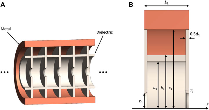
FIGURE 1. (A) Conceptual schematic of an infinite DAA structure. (B) Longitudinal cross section geometry of a regular cell of a DAA acelerator structure.
DAA design starts by optimizing parameters for the regular cell in order to maximize the Q0 and the Zeff for the resonant frequency of interest. The longitudinal cross section of the regular cell can be seen in Figure 1, where r0 is the aperture radius, rc is the corner fillet radius, a1 is the inner radius, b1 is the outer radius, c1 is the copper waveguide radius, d1 is the dielectric disk thickness, also known as iris, and L1 is the constant periodic length.
Once L1, r0 and rc are selected based on criteria explained later, the combination of a1, b1, c1 and d1 determines the figures of merit in the cavity, such as resonant frequency, quality factor and shunt impedance of the accelerating mode TM02-π. Thus, in this paper a new step is added to the optimization analysis, looking for the value of d1 which, in combination with the three radius selection, maximizes the shunt impedance of the cavity, in spite of fixing this value to
The resonant frequency goal was fixed at f0 = (3,000 ± 2) MHz, L1 = βλ0/2, r0 = 2 mm for comparison with high gradient copper structures and rc = d1/2. Then, in order to find the best values for d1 and the radii a1, b1, c1, a two step scan needs to be done. First, d1 is fixed at its initial value
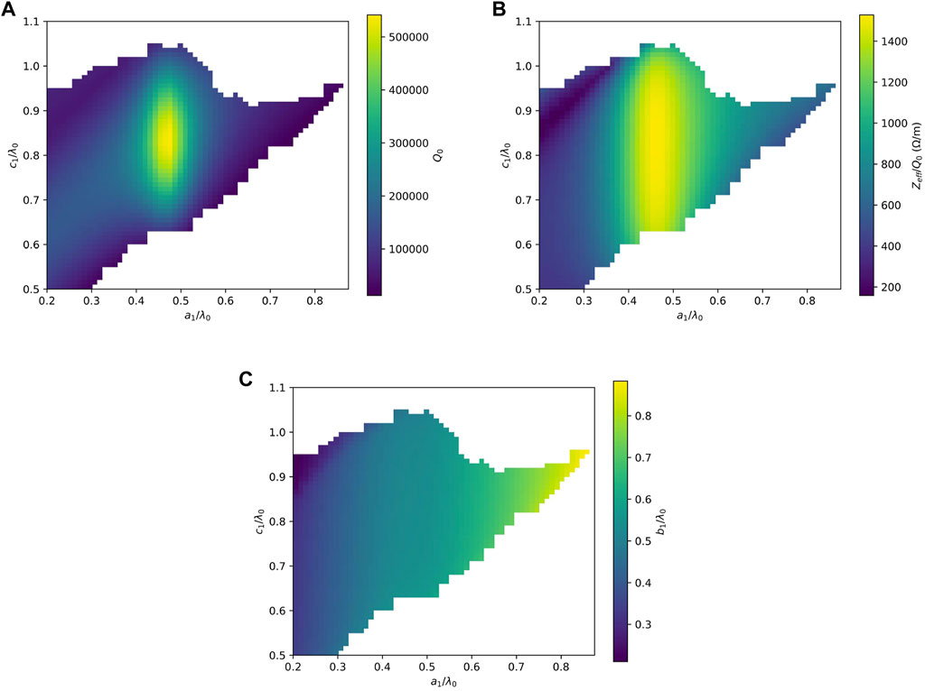
FIGURE 2. Numerical unloaded quality factor Q0 (A), shunt impedance over quality factor Zeff/Q0 (B) and geometric parameter b1 (C) as a function of geometrical parameters a1 and c1 for a regular cell using ideal dielectric MgTiO3 and β = 0.6. White region is due to the absence of a valid solution for the geometry.
This process is repeated for each value of a second swept in d1 = ξd0, where ξ is the normalized iris thickness. This allows to find a better solution in terms of Zeff, as illustrated in Figure 3 for MgTiO3 with ɛr = 16.66 and tan δ = 3.43 × 10⁻⁵.
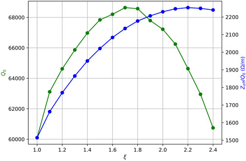
FIGURE 3. Numerical unloaded quality factor Q0 and shunt impedance over quality factor Zeff/Q0 as a function of normalized iris thickness for a regular cell using real dielectric MgTiO3 and β = 0.6.
The ratio of the peak electric field Ep and the peak magnetic field Hp to the average accelerating electric field Ea usually limits the achievable accelerating gradient for conventional iris-loaded metallic structures, where
where Ez is the longitudinal component of the electric field, ω = 2πf is the angular frequency and z is the longitudinal spatial coordinate. Field profiles for this structure are illustrated in Figure 4.
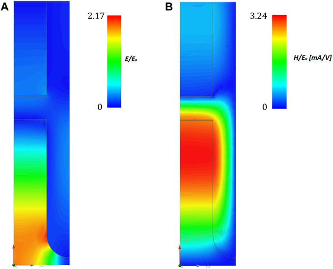
FIGURE 4. Electric field distribution E/Ea (A) and magnetic field distribution H/Ea (B) for the accelerating mode TM02-π in a half regular cell using MgTiO3, β = 0.6 and ξ = 2.
An optimization was done using four different ceramics that have been already used for RF dielectric cavities [11, 16, 40], whose electromagnetic properties can be found in Table 1, and particle velocity β = {0.4, 0.5, 0.6, 0.7, 0.8, 0.9, 1}. During these studies, it was observed that the geometry optimization depends mainly on the particle velocity β and the relative electric permittivity ɛr of the ceramic, while loss tangent tan δ determines the final value of Q0 as well as Zeff.
Energy ranges for Hadrontherapy treatments vary between 70 and 230 MeV for protons and 100–430 MeV/u for carbon ions, which correspond to particle velocities between 0.37–0.60 and 0.43–0.73, respectively [46]. Final results for the figures of merit for these designs, taking into account dielectric losses, are compared with an extension for all particle velocities of a high-gradient standing wave copper cavity designed for protons with β = 0.38 [47], as it can be seen in Figure 5.
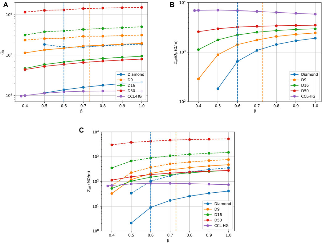
FIGURE 5. Final results for Q0 (A), Zeff/Q0 (B) and Zeff (C) for the different values of particle velocity and different material in the ideal case (dashed lines), and taking into account dielectric losses (solid lines). Vertical dashed lines correspond to the maximum energy of protons (blue) and carbon ions (orange). The results are compared with a high-gradient cell coupled linac CCL-HG copper cavity (purple line) [47].
A summary of the geometrical and electromagnetic parameters is included in Table 2.
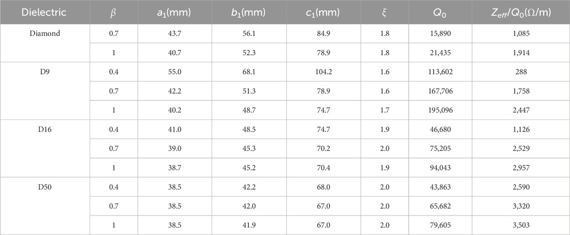
TABLE 2. List of optimum results for a selection of geometries.
Note the difference on the performance between the ideal and relativistic case. For the ideal case, the Q0 is over two orders of magnitude higher compared to HG copper structures. As it can be seen in Figure 5, the Q0 increases with ɛr and it is very sensitive to losses in the dielectric, though results are better than normal copper cavities. One caveat of this design is that a high amount of electrical energy is stored inside the dielectric, which is not going to be used to accelerate the beam. As a consequence, energy efficiency worsens, resulting in lower values of Zeff/Q0. Energy efficiency improves for larger ɛr and, as expected, does not depend on the dielectric tan δ. The performance of the structure will be given by the shunt impedance, which is a compromise between Q0 and Zeff/Q0. For the ideal case, the final result will be better for higher ɛr. However, due to the high sensitivity of Q0 with dielectric losses, the characteristic value of tan δ of the material is crucial on the real performance of the final structure. In addition, the performance increases also for higher particle velocities.
3 Results
Once the optimization of the geometry has been performed, the electromagnetic performance of the regular cell has to be considered as a component of a real accelerator system. In order to do so, electromagnetic losses are studied in detail as well as the dispersion relation of the regular cell. In addition, the field instabilities and singularities which can lead to multipactor or RF breakdown discharges are taking into account to minimize risk at high power test. Besides, the consequences of using coating to suppress multipactor in the RF performance is also deliberated.
3.1 Dielectric loss tangent
The advantage of working under the TM02-π mode, is that metallic losses are highly suppressed and, consequently, the DAA regular cell performance will be determined mainly by the quality of the dielectric in terms of its tan δ.
Dielectric and metallic losses are given by [39],
respectively, where
A graphical representation of both surface and volumetric loss densities are illustrated in Figure 6. As the loss tangent depends strongly on the manufacturing process for the ceramic fabrication, values of Table 1 are just references from previous experimental measurements. Therefore, it is of great importance to study the dependence of regular cell performance as a function of the tan δ of the material, as illustrated in Figure 6, where an exponential decrease of the cavity performance can be seen for values of tan δ > 10–5.
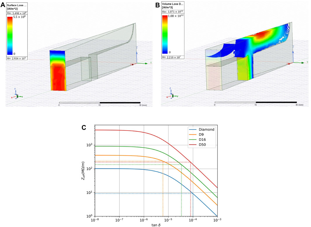
FIGURE 6. Surface metallic losses (A) and volumetric dielectric losses (B) density for accelerating mode TM02-π in a regular cell using MgTiO3, β = 0.6, stored electromagnetic energy W = 1 J and ξ = 2. Shunt impedance as a function of tan δ (C) for different materials and β = 0.6. Experimental tan δ values for each material are shown.
3.2 Dispersion relation
The overlapping between adjacent modes is a typical problem from the tunability and operational point of view for periodic RF accelerating structures, which is the case for the standing-wave accelerating structure studied in this work. In addition, good electromagnetic coupling between consecutive cells is also a key factor in order to determine the maximum number of cells per cavity.
Electric coupling between consecutive cells improves for lower electric permittivity and particle velocity, as it is illustrated in Figure 7. It can be observed that the TM02 mode is strongly electrically coupled, so there is no need for coupling cells between regular cells.
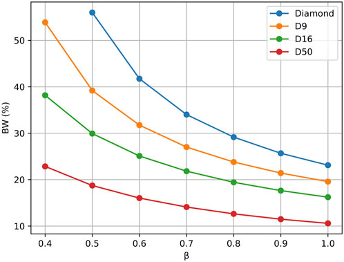
FIGURE 7. Electrical coupling bandwidth for different materials and particle velocities with normalized iris thickness ξ = 1.5. The bandwidth is defined as BW = (fπ − f0)/fπ ⋅ 100%, where fπ and f0 are the resonant frequencies of π and 0 mode respectively.
Dispersion curves for the second order mode and the next higher frequency axisymmetric mode are depicted in Figure 8 for each material for two different normalized iris thickness. It can be seen that for low electric permittivity material, the higher order mode crosses the 3 GHz point and, therefore, overlapping cannot be avoided. In addition, as the iris becomes thicker, it can be seen that higher order modes with a phase advance of π get closer to the resonant frequency and they can even cross this point for thicker irises. Consequently, electric permittivity and normalized iris thickness are bounded by the overlapping process.
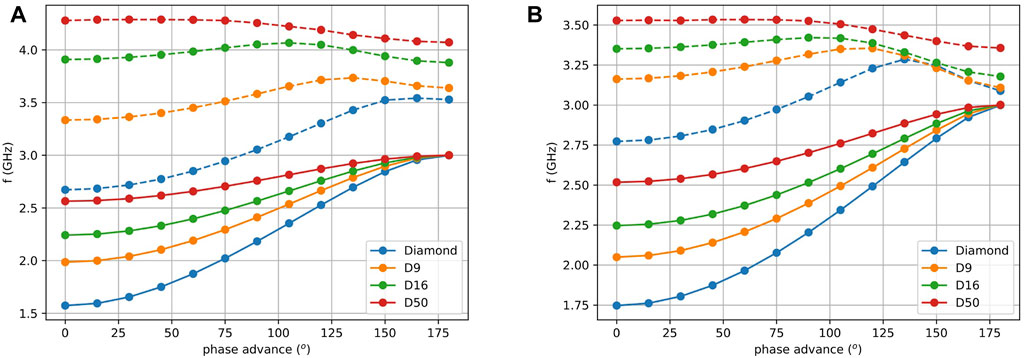
FIGURE 8. Dispersion curve of the accelerating mode TM02 (solid line) and next higher frequency axisymmetric mode (dashed line) for different dielectric materials and β = 0.6 and normalized iris thickness ξ = 1 (A) and ξ = 1.5 (B).
A field distribution of the higher frequency modes are shown in Figure 9 for a phase advanced of 0°, which corresponds to the mode TM03 at f = 3.354 GHz and for a phase advance of 180°, corresponding with a dielectric mode at f = 3.184 GHz.
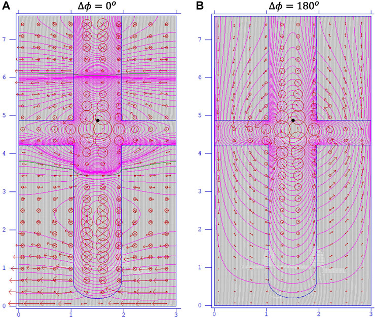
FIGURE 9. Next higher frequency axisymmetric mode for Δϕ = 0° at f = 3.354 GHz (A) and Δϕ = 180° at f = 3.184 GHz (B) for D16, β = 0.6 and ξ = 1.5.
3.3 Surface field studies
As it is shown in Figure 10, Ep/Ea for the optimal geometry decreases with the material permittivity and particle velocity and it is always below 4 which is the value obtained for CCL-HG cavity [47]. This ratio is one of the main limiting factors for HG cavities, since it is related with breakdowns production. Besides, it was observed that this ratio also decreases for thinner irises. Therefore, the performance of the DAA regular cell improves with particle velocity and higher electric permittivity being able to improve current values for room-temperature copper cavities.
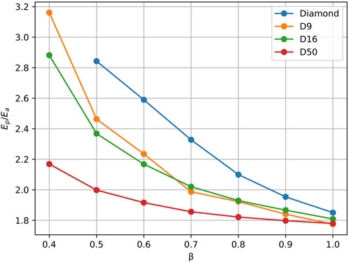
FIGURE 10. Ratio of peak electric field and average accelerating field for different materials and particle velocities.
The existence of sharp angles and triple junction points in the original design can lead to singularities in the surface electric field. As a consequence, field instabilities, RF breakdowns or multipactor discharges can emerge.
Regarding the triple junction point (point B in Figure 11), assuming zero conductivity in dielectric and flat metal wall, the electric field increases as |E|∝ rn−1, where r is the radial distance to the triple junction point and n follows [19]:
where α is the angle of vacuum between dielectric and metal and ɛr is the relative electric permittivity of the dielectric.
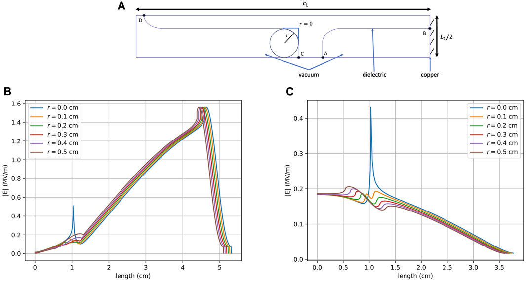
FIGURE 11. (A) Geometry modification. Electric field magnitude along path CD (B) and AB (C) for different corner radius for D16. Electric field is normalized for 1 MV/m of accelerating voltage.
From Eq. 4 it can be concluded that if α < 90° then n < 1, leading to infinitely large electric field in the junction, whereas if α > 90° then n > 1, leading to null electric field. Only the case with α = 90° leads to n = 1, implying a non-zero and non-singular value. However, we are just interested in avoiding singularities, which can be achieved by adjusting α ≥ 90°, which was already satisfied in the original design. In addition, sharp metallic corners are another source of field singularities which must be avoided.
Regarding the dielectric corners in the junction between the dielectric ring and the iris, it was observed that sharp geometries also lead to field divergences. Thus, the geometry was changed as shown in Figure 11 and the surface electric field for different round corners was studied for a fine mesh, as illustrated in Figure 11. In addition, this changes produced a slight increase in the Zeff.
3.4 Coating effects
Amorphous Carbon (a-C) and Diamond Like Carbon (DLC) coatings were studied at Conseil Européen pour la Recherche Nucléaire (CERN) for Secondary Electron Yield (SEY) reduction in order to avoid multipactor discharges [48]. However, surface losses on the coating will have an impact on the electromagnetic performance of the cavity. These losses are given by
where R is the sheet surface resistance of the coating.
Figure 12 illustrates Q0 as a function of the sheet resistance (in ohms per □) for different cases: no coating, dielectric fully covered with coating, internal coating (which corresponds with coating in region CD) and external coating (which corresponds with coating in region AB). The surface resistance of DLC coating was above 1 MΩ per □ and could not be measured, while a-C samples measurements are marked with black dashed lines.
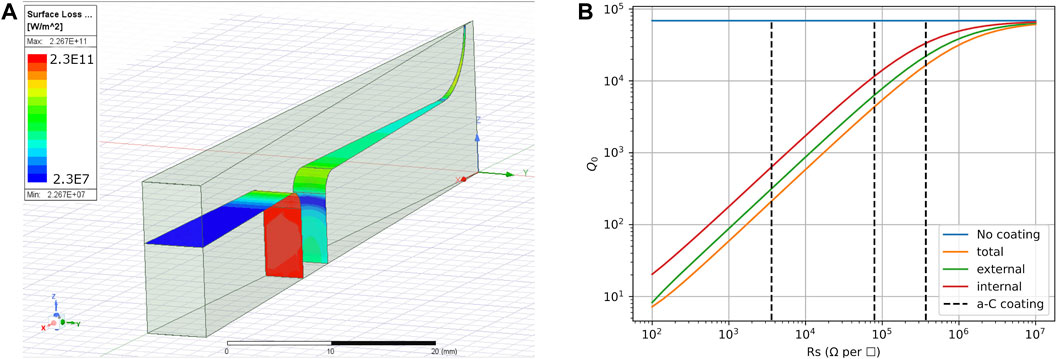
FIGURE 12. (A) Graphical representation of coating losses in logarithmic scale for a sheet resistance Rs = 37,000 Ω per □ for D16, β = 0.6, ξ = 2 and W = 1 J. (B) Comparison of unloaded quality factor of a regular cell partially coated in the external or internal regions of the cavity, full covered and without coating as a function of the sheet resistance.
As it can be observed in Figure 12, Q0 rapidly decreases for low resistance coatings and therefore thin films or materials with high resistivity are useful coatings to improve the electromagnetic performance.
3.5 Thermal simulations
In order to estimate the required cooling system and the mechanical stress and deformation induced by RF losses, thermal simulations were carried out using the ANSYS software [49]. Volumetric and surface losses were used as input for steady thermal simulations with 3 cm of copper wall fixing the external temperature at 22°C as boundary condition. Simulations were done for different geometries and ceramics, as illustrated in Table 3. Ultra high pure alumina was used for simulations instead of MgO and BaTiOx because of its higher thermal conductivity in order to evaluate three different meaningful values.
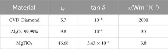
TABLE 3. List of dielectrics used for thermal simulations.
For numerical simulations, an accelerating gradient of 50 MV/m was used, with a duty cycle D = 0.075 × 10⁻³. The duty cycle is defined as
where τ is the pulse width and T is the total period of the signal. A graphical solution for Al2O3 for β = 1 is shown in Figure 13.
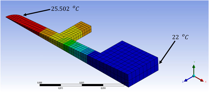
FIGURE 13. Steady temperature distribution for Al2O3 and β = 1.
As shown in Figure 13, the maximum temperature is reached close to the aperture of the ceramic, with a decreasing temperature gradient towards the copper metallic enclosure, which barely changes thanks to its high thermal conductivity (κ = 400 W⋅ m−1⋅ K−1). The maximum temperature reached for different geometries and materials is illustrated in Figure 14.
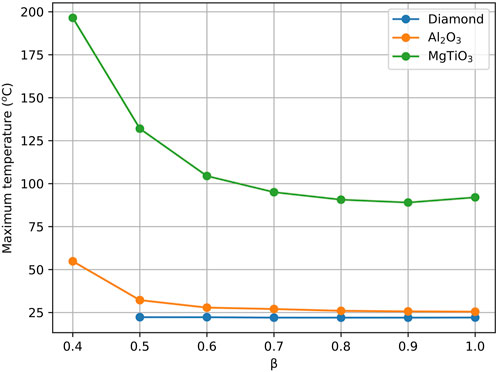
FIGURE 14. Maximum temperature reached for different ceramics and particle velocities.
The temperature is higher for lower particle velocity while it seems to saturate at around β = 0.7 following the behaviour of the Zeff. In addition, very low thermal conductivity, as in MgTiO3, leads to temperatures beyond acceptable limits regarding stress and deformation tolerances, even though we are still far from the fusion point.
4 Conclusion
DAA structures for low β particles have been studied for the first time, proving the potential to improve the performance of current room-temperature copper cavities. This study shows improvements in the optimization process and optimal results for an S-band DAA cavity as a solution for compact linear accelerators for Hadrontherapy treatments.
Working under the TM02-π mode, copper ohmic losses can be highly reduced by accumulating electrical energy inside the dielectric. From these studies we could conclude that cavity efficiency increases for higher particle velocity and electric permittivity. However, due to the high energy density inside the dielectric, the cavity performance will be limited by dielectric losses. Therefore, reaching low dielectric loss tangent is a fundamental key in the fabrication of ceramics in particular for DAA cavities.
Iris thickness plays also a fundamental role in the cell optimization by increasing the accelerating voltage and also by reducing the electric energy density inside the ceramic by decreasing dielectric losses. As a consequence, materials with higher loss tangent have thicker optimum irises than ideal geometries.
In addition, the low Ep in metallic walls in combination with high breakdown threshold of dielectrics, potentially allow DAA cavities to reach higher gradients without producing RF breakdowns, after multipactor suppression. This ratio decreases for high particle velocity, high electric permittivity and thin irises.
High electric coupling between consecutive cells has been observed for all kind of geometries. In addition, it was shown that coupling improves for lower particle velocity and lower electric permittivity. However low electric permittivity materials, such as CVD diamond, suffer from mode overlapping. In addition, thicker irises produce the excitation of more modes whose resonant frequencies are close to our operational frequency. As a result, the final design must find a compromise between an optimum electromagnetic design, which is achieved for thicker irises and low mode overlapping and low peak electric field, which improve for thinner irises.
Dielectric corners have been rounded in order to smooth the surface electric field. Moreover, stability studies of triple junction point were performed concluding that in order to avoid electric field singularities, the vacuum angle between dielectric and copper must be α ≥ 90° and metallic sharp angles must be avoided.
Multipactor is one of the main limitations of DLA cavities due to high SEY of ceramics. Because of that, thin coating with low SEY is used for multipactor suppression. However, surface resistance of coating will have an effect on RF performance that must be studied in advance. Numerical simulations showed that low resistance coatings are unacceptable from an electromagnetic point of view, which implies that only high resistance materials or very thin coatings can be used in order to reduce multipactor.
Finally, thermal conductivity of the ceramic is found to be a crucial parameter also on the design to avoid overheating of the cavity leading to high deformation and stress. Thus, a lower bound value is set around 20–30 W⋅ m−1⋅ K−1 depending on particle velocity and duty cycle.
Data availability statement
The raw data supporting the conclusion of this article will be made available by the authors, without undue reservation.
Author contributions
PM-R: Conceptualization, Formal analysis, Software, Writing–original draft. DE: Conceptualization, Supervision, Funding acquistion, Writing–review and editing. AG: Conceptualization, Methodology, Supervision, Funding acquistion, Writing–review and editing. BG: Conceptualization, Supervision, Funding acquistion, Writing–review and editing. CB: Writing–review and editing. DG-I: Writing–review and editing. NF-M: Writing–review and editing. PM-L: Writing–review and editing. EM: Writing–review and editing. AM: Writing–review and editing. JF: Funding acquistion, Writing–review and editing.
Funding
The author(s) declare financial support was received for the research, authorship, and/or publication of this article. Work supported by Ministerio de Universidades (Gobierno de España) under grant number FPU19/00585 and EST22/00739. The authors declare that this study received funding from CERN.
Conflict of interest
AG was employed by CERN.
The remaining authors declare that the research was conducted in the absence of any commercial or financial relationships that could be construed as a potential conflict of interest.
Publisher’s note
All claims expressed in this article are solely those of the authors and do not necessarily represent those of their affiliated organizations, or those of the publisher, the editors and the reviewers. Any product that may be evaluated in this article, or claim that may be made by its manufacturer, is not guaranteed or endorsed by the publisher.
References
1. Shintake T, Tanaka H, Hara T, Tanaka T, Togawa K, Yabashi M, et al. A compact free-electron laser for generating coherent radiation in the extreme ultraviolet region. Nat Photon (2008) 2:555–9. doi:10.1038/nphoton.2008.134
2. Tanabe E, Fineberg Y, Matsumoto H, Shintake T. Medical applications of c-band accelerator technologies. Proc Linear Accel Conf (1998) 627–9.
3. Sethi R. Electron beam accelerators for materials processing: a barc scenatrio. Proc APAC (2004) 708–10.
4. Aicheler M, Burrows P, Draper M, Garvey T, Lebrun P, Peach K, et al. A multi-tev linear collider based on clic technology: Clic conceptual design report. Menlo Park, CA (United States): SLAC National Accelerator Lab. (2014). Tech. rep.
5. Degiovanni A, Amaldi U, Bonomi R, Garlasché M, Garonna A, Verdú-Andrés S, et al. Tera high gradient test program of rf cavities for medical linear accelerators. Nucl Instr Methods Phys Res Section A: Acc Spectrometers, Detectors Associated Equipment (2011) 657:55–8. doi:10.1016/j.nima.2011.05.014
6. Benedetti S. High-gradient and high-efficiency linear accelerators for hadron therapy. Switzerland: Ph.D. thesis, Ecole Polytechnique Fédérale de Lausanne (2018).
7. Vnuchenko A. High-gradient issues in S-band RF acceleration structure for hadrontherapy accelerators and radio frequency Quadrupoles. Spain: Ph.D. thesis, University of Valencia (2020).
8. Gai W, Konecny R, Simpson J. Externally powered dielectric loaded waveguides as accelerating structures. In: Proceedings of the 1997 particle accelerator Conference (Cat. No. 97CH36167), 1. IEEE (1997). p. 636–8.
9. Liu W, Jing C, Gai W, Konecny R, Power J. New rf design for 11.4 ghz dielectric loaded accelerator. In: Proceedings of the 2003 particle accelerator Conference (IEEE), 3 (2003). p. 1810–2.
10. Gold S, Jing C, Kanareykin A, Gai W, Konecny R, Liu W, et al. Development and testing of x-band dielectric-loaded accelerating structures. Proc Part Accel Conf (2010) 3001–3. doi:10.1063/1.3520330
11. Wei Y, Grudiev A, Freemire B, Jing C. A compact, low-field, broadband matching section for externally powered x-band dielectric-loaded accelerating structures. IEEE Trans Nucl Sci (2022) 69:991–1001. doi:10.1109/tns.2022.3159028
12. Wei Y, Bursali H, Grudiev A, Freemire B, Jing C, Wegner R, et al. Design, fabrication, and low-power rf measurement of an x-band dielectric-loaded accelerating structure. Phys Rev Acc Beams (2022) 25:041301. doi:10.1103/physrevaccelbeams.25.041301
13. Thompson M, Badakov H, Cook A, Rosenzweig J, Tikhoplav R, Travish G, et al. Breakdown limits on gigavolt-per-meter electron-beam-driven wakefields in dielectric structures. Phys Rev Lett (2008) 100:214801. doi:10.1103/physrevlett.100.214801
14. Jing C, Gai W, Power J, Konecny R, Gold SH, Liu W, et al. High-power rf tests on x-band dielectric-loaded accelerating structures. IEEE Trans plasma Sci (2005) 33:1155–60. doi:10.1109/TPS.2005.851957
15. Jing C, Gai W, Power JG, Konecny R, Liu W, Gold SH, et al. Progress toward externally powered x-band dielectric-loaded accelerating structures. IEEE Trans plasma Sci (2010) 38:1354–60. doi:10.1109/TPS.2009.2036921
16. Freemire B, Shao J, Weatherly S, Peng M, Wisniewski E, Doran S, et al. Development of x-band single-cell dielectric disk accelerating structures. Phys Rev Acc Beams (2023) 26:071301. doi:10.1103/physrevaccelbeams.26.071301
17. Jing C, Chang C, Gold S, Konecny R, Antipov S, Schoessow P, et al. Observation of multipactor suppression in a dielectric-loaded accelerating structure using an applied axial magnetic field. Appl Phys Lett (2013) 103:213503. doi:10.1063/1.4832326
18. Jing C, Gold S, Fischer R, Gai W. Complete multipactor suppression in an x-band dielectric-loaded accelerating structure. Appl Phys Lett (2016) 108:193501. doi:10.1063/1.4949334
19. Techaumnat B, Hamada S, Takuma T. Effect of conductivity in triple-junction problems. J electrostatics (2002) 56:67–76. doi:10.1016/s0304-3886(01)00219-4
20. Freemire B, Jing C, Poddar S, Beamlabs E, Zhao Y, Techlabs E, et al. High power test of a dielectric disk loaded accelerator for a two beam wakefield accelerator. In: 12th International particle accelerator Conference (IPAC’21). Geneva, Switzerland: JACOW Publishing (2021). p. 1096–9. Campinas, SP, Brazil, 24-28 May 2021.
21. Frankel S. Tm 0, 1 mode in circular wave guides with two coaxial dielectrics. J Appl Phys (1947) 18:650–5. doi:10.1063/1.1697821
22. Bruck G, Wicher E. Slow transverse magnetic waves in cylindrical guides. J Appl Phys (1947) 18:766–9. doi:10.1063/1.1697834
23. Oliner A. Remarks on slow waves in cylindrical guides. J Appl Phys (1948) 19:109–10. doi:10.1063/1.1697862
24. Harvie RS. A proposed new form of dielectric-loaded wave-guide for linear electron accelerators. Nature (1948) 162:890. doi:10.1038/162890a0
25. Cohn G, Flesher G. Design construction and initial operation of a continuous dielectric loaded linear accelerator. Electron Res Laboratories, Ill Inst. Technol. Chicago, IL, USA, Tech. Rep (1952) 2.
26. Mullett L, Walkinshaw W, Bell J, Loach B, Shersby-Harvie R. A theoretical and experimental investigation of anisotropic-dielectric-loaded linear electron accelerators. Proc IEE-B: Radio Electron Eng (1957) 104:273–90. doi:10.1049/pi-b-1.1957.0152
27. Walker G, Lewis E. Vacuum breakdown in dielectric-loaded wave-guides. Nature (1958) 181:38–9. doi:10.1038/181038b0
28. Woode R, Ivanov E, Tobar M, Blair D. The measurement of the dielectric loss tangent of alumina at microwave frequencies and room temperature. Electronics Lett (1994) 30:2120–2. doi:10.1049/el:19941470
29. Alford NM, Penn SJ. Sintered alumina with low dielectric loss. J Appl Phys (1996) 80:5895–8. doi:10.1063/1.363584
30. Huang CL, Wang JJ, Huang CY. Microwave dielectric properties of sintered alumina using nano-scaled powders of α alumina and tio2. J Am Ceram Soc (2007) 90:1487–93. doi:10.1111/j.1551-2916.2007.01557.x
31. Templeton A, Wang X, Penn SJ, Webb SJ, Cohen LF, Alford NM. Microwave dielectric loss of titanium oxide. J Am Ceram Soc (2000) 83:95–100. doi:10.1111/j.1151-2916.2000.tb01154.x
32. Breeze JD, Aupi X, Alford NM. Ultralow loss polycrystalline alumina. Appl Phys Lett (2002) 81:5021–3. doi:10.1063/1.1532553
33. Kanareykin A. New advanced dielectric materials for accelerator applications. In: AIP Conference Proceedings (American Institute of Physics), 1299 (2010). p. 286–91.
34. Jing C, Kanareykin A, Kazakov S, Liu W, Nenasheva E, Schoessow P, et al. Development of a dual-layered dielectric-loaded accelerating structure. Nucl Instr Methods Phys Res Section A: Acc Spectrometers, Detectors Associated Equipment (2008) 594:132–9. doi:10.1016/j.nima.2008.06.037
35. Zou P, Xiao L, Sun X, Gai W, Wong T. Hybrid dielectric and iris-loaded periodic accelerating structure. J Appl Phys (2001) 90:2017–23. doi:10.1063/1.1383578
36. Shao J, Jing C, Power J, Conde M, Doran D. Study of a dielectric disk structure for short pulse two-beam acceleration. Group (2018) 1:4. doi:10.18429/JACoW-IPAC2018-TUPML005
37. Power J, Gai W, Gold S, Kinkead A, Konecny R, Jing C, et al. Observation of multipactor in an alumina-based dielectric-loaded accelerating structure. Phys Rev Lett (2004) 92:164801. doi:10.1103/physrevlett.92.164801
38. Jing C, Kanareykin A, Power J, Conde M, Yusof Z, Gai W. Observation of enhanced transformer ratio in collinear wakefield acceleration. In: AIP Conference Proceedings (American Institute of Physics), 877 (2006). p. 511–9.
39. Satoh D, Yoshida M, Hayashizaki N. Dielectric assist accelerating structure. Phys Rev Acc Beams (2016) 19:011302. doi:10.1103/physrevaccelbeams.19.011302
40. Satoh D, Yoshida HNM, Hayashizaki N. Fabrication and cold test of dielectric assist accelerating structure. Phys Rev Acc Beams (2017) 20:091302. doi:10.1103/physrevaccelbeams.20.091302
41. Mori S, Yoshida M, Satoh D. Multipactor suppression in dielectric-assist accelerating structures via diamondlike carbon coatings. Phys Rev Acc Beams (2021) 24:022001. doi:10.1103/physrevaccelbeams.24.022001
42. Wei Y, Grudiev A. Investigations into x-band dielectric assist accelerating structures for future linear accelerators. IEEE Trans Nucl Sci (2021) 68:1062–71. doi:10.1109/tns.2021.3069110
43. Braccini S. Scientific and technological development of hadrontherapy. In: Astroparticle, particle and space Physics, Detectors and medical Physics applications. World Scientific (2010). p. 598–609.
44. Halbach K, Holsiger RF. Superfish - a computer program for evaluation of rf cavities with cylindrical symmetry. Part Acc (1976) 7:213–22.
45. ANSYS HFSS software. ANSYS HFSS software (2023). Available at: http://www.ansoft.com/products/hf/hfss (Accessed October 31, 2023).
46. Bencini V. Design of a novel linear accelerator for carbon ion therapy. Rome U.: Ph.D. thesis (2020).
47. Benedetti S, Grudiev A, Latina A. High gradient linac for proton therapy. Phys Rev Acc Beams (2017) 20:040101. doi:10.1103/physrevaccelbeams.20.040101
48. Grudiev A, Poddar S, Neupert H, Vollenberg W, Freemire B, Jing C. Amorphous and diamond-like carbon coatings for sey reduction of dielectric materials for accelerating structure applications. Tech Rep (2022).
49. ANSYS software. ANSYS software (2023). Available at: https://www.ansys.com (Accessed October 31, 2023).
Keywords: dielectric assist accelerating (DAA) structures, radio frequency (RF), LINAC, hadrontherapy, standing wave
Citation: Martinez-Reviriego P, Esperante D, Grudiev A, Gimeno B, Blanch C, González-Iglesias D, Fuster-Martínez N, Martín-Luna P, Martínez E, Menendez A and Fuster J (2024) Dielectric assist accelerating structures for compact linear accelerators of low energy particles in hadrontherapy treatments. Front. Phys. 12:1345237. doi: 10.3389/fphy.2024.1345237
Received: 27 November 2023; Accepted: 18 January 2024;
Published: 02 February 2024.
Edited by:
Weihao Liu, Nanjing University of Aeronautics and Astronautics, ChinaReviewed by:
Giuseppe Torrisi, Laboratori Nazionali del Sud (INFN), ItalyHsin Yu Yao, National Chung Cheng University, Taiwan
Copyright © 2024 Martinez-Reviriego, Esperante, Grudiev, Gimeno, Blanch, González-Iglesias, Fuster-Martínez, Martín-Luna, Martínez, Menendez and Fuster. This is an open-access article distributed under the terms of the Creative Commons Attribution License (CC BY). The use, distribution or reproduction in other forums is permitted, provided the original author(s) and the copyright owner(s) are credited and that the original publication in this journal is cited, in accordance with accepted academic practice. No use, distribution or reproduction is permitted which does not comply with these terms.
*Correspondence: Pablo Martinez-Reviriego, cGFibG8ubWFydGluZXoucmV2aXJpZWdvQGlmaWMudXYuZXM=