 S. C. Lee
 H. J. Hyun
 J. M. Baek
 S. M. Hwang1
95% of researchers rate our articles as excellent or good
Learn more about the work of our research integrity team to safeguard the quality of each article we publish.
Find out more
ORIGINAL RESEARCH article
Front. Phys. , 04 January 2024
Sec. Radiation Detectors and Imaging
Volume 11 - 2023 | https://doi.org/10.3389/fphy.2023.1328639
This article is part of the Research Topic Pushing Frontiers - Imaging For Photon Science View all 19 articles
The Pohang-Accelerator-Laboratory X-ray free-electron laser (PAL-XFEL) emits intense, ultra-short X-ray pulses, enabling studies on ultra-small and -fast dynamics in various fields. We designed and fabricated silicon p-intrinsic-n photo-diodes (PDs) to detect strong X-ray pulses. Four types of PDs were fabricated with different metal shapes on the P- and N-sides. The fabrication process was split into two parts, based on the thickness of the Al metal and anti-reflective coating (ARC) layers, to evaluate the fabrication process feasibility and the detection performance. A beam test was performed with X-ray pulses at the soft X-ray beamline of the PAL-XFEL using the proposed PDs and a commercial PD. The test was designed to evaluate the effects of the metal and ARC layers and compare the detection efficiency depending on the X-ray entrance side and signal readout side. The waveforms were saved during the test and integrated to obtain the charges. Thereafter, they were analyzed and normalized, and compared. This paper presents the preparation, setup, and procedure of the beam test, and the test results are described.
The Pohang-Accelerator-Laboratory X-ray free-electron laser (PAL-XFEL) [1, 2] is a scientific research facility that provides intense, ultra-short, and coherent X-ray pulses, typically generated through self-amplified spontaneous emission (SASE) process [3, 4]. The PAL-XFEL has recently begun offering hard X-ray self-seeded FELs [5] for specific experiments that require a narrow bandwidth and high spectral brightness. The PAL-XFEL comprises a hard X-ray (HX) beamline [6] and a soft X-ray (SX) beamline [7, 8]. The HX and SX beamlines operates with photon energies in the ranges of 2–15 keV and 0.25–1.25 keV, respectively. The unique properties of XFEL beams enable the study of ultra-small and -fast dynamics in various fields through pump-probe experiments [9]. Optical laser pump with wavelengths of 266, 400, or 800 nm and X-ray probe experiments are commonly conducted at the PAL-XFEL.
The XFEL beam unpredictably fluctuates between pulses because of the SASE process; thus, online photon diagnostics is essential. As representative online diagnostics devices, the quadrant beam position monitor (QBPM) and gas monitor detector (GMD) are used at the HX and SX beamlines, respectively. The QBPM comprises four photo-diodes (PDs) and a thin film in the beam path [10, 11]. The operation of the GMD is based on the photo-ionization of noble gases [12]. In addition, PDs are used in various ways at both beamlines as destructive or non-destructive methods, including beam alignment, beam size measurement, timing jitter measurement, and scattering signal measurement (a method for normalizing experimental data).
The PDs used at the PAL-XFEL are commercial, and it can be challenging to optimize their specifications for various purposes and obtain them on time owing to external factors, such as international circumstances. Thus, we designed and fabricated PDs for strong X-ray and optical laser detection at the foundries of institutes in South Korea using an N-type silicon substrate with a thickness of 500 μm, diameter of 6 inches, and high resistivity (more than 5 kΩ⋅cm). We designed four types of p-intrinsic-n (PIN) PDs depending on the metal structure on the P-side (junction side, signal readout) and N-side (ohmic side, light entrance window). The metal on each side was designed as a ring or whole shape and labeled as Pr (P-side ring), Pw (P-side whole), Nr (N-side ring), or Nw (N-side whole). Anti-reflective coating (ARC) was applied to the N-side to reduce the reflection of visible light. A thick SiO2 layer was deposited on the P-side to protect it from environmental degradation. Figure 1 shows the different metal types used on the P- and N-sides. The fabricated PDs have been previously characterized [13] in terms of design, fabrication, electrical characteristics, quantum efficiency, signal-to-noise ratio, and energy resolution. The PDs were evaluated for the effects of metal thickness and detection efficiency using an XFEL beam. This paper presents the electrical characteristics of selected PDs for an X-ray beam test and describes the test results depending on the metal and readout types of the PDs, including the existence of the ARC layer. The fabricated PDs were compared with a commercial PD (S3590-09, Hamamatsu (HPK-PD) [14]).
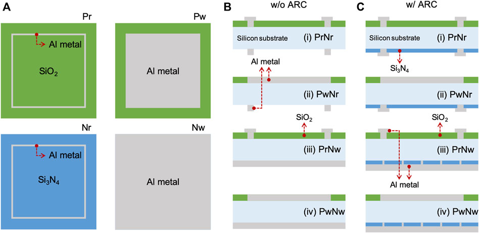
FIGURE 1. (A) Simple schematics of four metal types; P- and N-side rings and whole metals and (B, C) cross-sectional views of their combinations; (i) PrNr, (ii) PwNr, (iii) PrNw, and (iv) PwNw depending on the existence of an ARC layer. In their schematics, sky blue represents the silicon substrate, green represents the passivation layer of SiO2, gray represents the Al metal layer, and blue represents the ARC layer of Si3N4. Pr had the SiO2 layer, and Nr may or may not have the Si3N4 layer depending on the ARC process. The implant region of Pw and Nw is covered by the Al metal layer.
The main purposes of the X-ray beam test with the fabricated PDs were to evaluate the effect of the metal thickness and ARC layer and compare the detection efficiencies of the fabricated PDs with that of the HPK-PD, depending on the light entrance and signal readout sides. Nine fabricated PDs were selected based on their electrical test results and categorized into Sets A (A-1 to A-5) and B (B-2 to B-5), to address the test objectives. The HPK-PD was designated B-1. The capacitance and leakage current of the PDs with good and similar electrical test results were measured using an LCZ meter (4277A, HP) and a picoammeter (6487, Keithley) (Figure 2). The measured capacitances at the full depletion voltage of 125.6 ± 4.9 V correlated with the calculated bulk capacitance of 20.7 ± 0.9 pF/cm2. The leakage currents of the PDs except A-4 and A-5 were below 10 nA/cm2 at the full depletion voltage. A printed circuit board (PCB) for detecting high intensity beams in the photoconductive mode was used to mount the PDs. The pads of the PCB were wire-bonded to the electrodes of the PDs for signal readout and biasing.
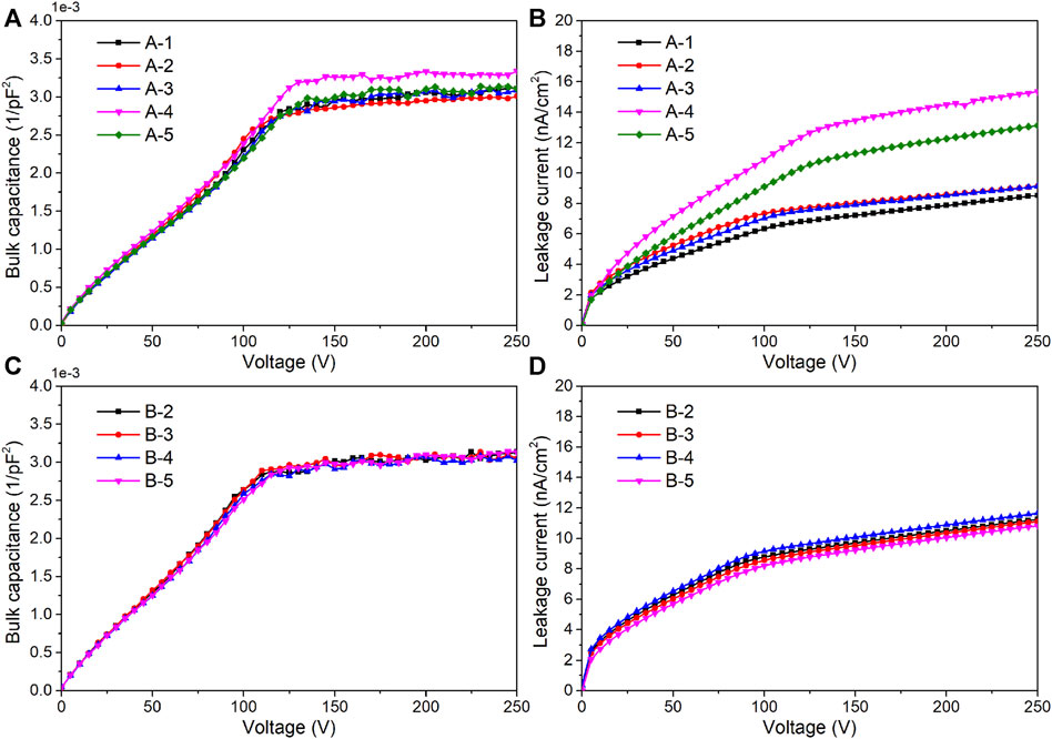
FIGURE 2. Electrical characteristics of fabricated PDs. (A, C) Capacitances and (B, D) leakage currents of Sets A and B.
Set A was used to evaluate the effects of the metal thickness and ARC layer on the N-side. Set A PDs were the Pw type and shared a common light entrance and signal readout configuration (X-ray entrance to the N-side and signal readout from the P-side). Table 1 lists the fabrication parameters of the metal and ARC layers of Set A. A-1 was of the Nr type, with no metal or ARC layers on its N-side (Figure 1B(ii)). A-2 and A-3 both had 150 nm-thick TiW layers and Al layers of 100 and 200 nm, respectively, on their N-sides (Figure 1B(iv)). The average thickness of the ARC layer on A-4 (Figure 1C(ii)) and A-5 (Figure 1C(iv)) was 48.3 ± 0.5 nm, as measured at five points on the wafer (top, bottom, left, right, and center). A-5 was of the Nw type with a metal stack of 150 nm-thick TiW and 400 nm-thick Al. The thicknesses of the Al layers were determined by measuring the sheet resistance of the Al at five points on the wafer, using the average sheet resistance and resistivity of Al (2.735 × 10⁻⁸ Ω⋅m). Set B comprised the HPK-PD (B-1) and four fabricated PrNr type PDs without metal or ARC layers (Figure 1B(i)), to examine the effects of the light entrance and signal readout sides on charge collection and rising time. Table 2 defines the light entrance and signal readout sides of each PD. B-1 and B-2 had the light entrance and signal readout on the P-side, whereas B-3 had the light entrance and signal readout on the P- and N-sides, respectively. B-4 was the opposite of B-3, and B-5 had the light entrance and signal readout on the N-side.
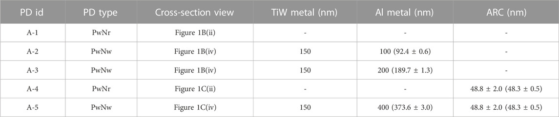
TABLE 1. Evaluating the effect of Al and ARC layers on the N-side. Set A comprised PwNr and PwNw structures, with cross-sectional views depicted in Figure 1B(ii), Figure 1C(ii), Figure 1B(iv), and Figure 1C(iv), respectively. The fabrication parameters for the Al metal and ARC layers in Set A, as well as the target and measured values are presented. Set A has light entrance on the N-side and signal readout on the P-side.
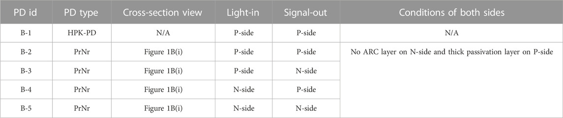
TABLE 2. Investigating the effect of light entrance and signal readout sides. Set B consisted of the HPK-PD and four fabricated PrNr type PDs, with cross-sectional views depicted in Figure 1B(i). Definitions of light entrance and signal readout sides of Set B are presented.
The X-ray beam test was performed at the SX beamline of the PAL-XFEL. Figure 3 shows the layout of the experimental hall of the SX beamline. A vacuum test chamber was installed between a resonant soft X-ray scattering (RSXS) endstation and an X-ray absorption and emission spectroscopy (XAS/XES) endstation. An X-Y manipulator was assembled on the test chamber, and Sets A and B were assembled in a holder and successively tested. Charge signals from the PDs were processed using a current amplifier (DHPCA-100, FEMTO) and a digitizer (PXIe-5160, National Instruments) synchronized with the PAL-XFEL event timing system. Figure 4 shows the vacuum test chamber installed on the SX beamline, with the PDs. Prior to the data acquisition, the PD holder was aligned, and the center position of each PD was recorded using the X-Y manipulator.
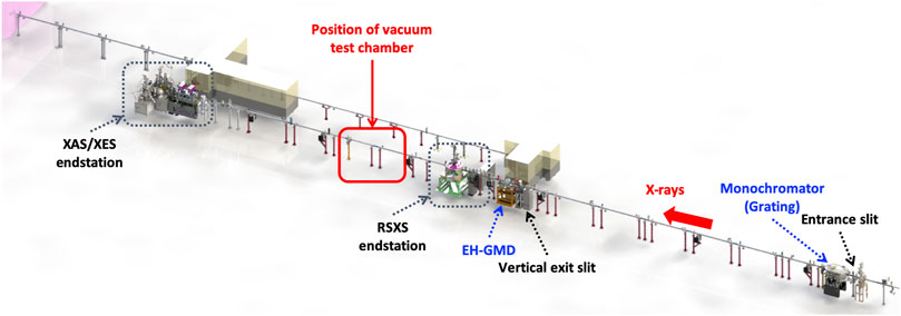
FIGURE 3. Layout of the experimental hall of the SX beamline.
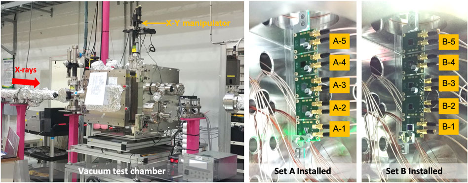
FIGURE 4. Vacuum test chamber installed downstream of the RSXS endstation with PDs from Sets A and B assembled inside.
Monochromatic photons with energies of 400, 500, 700, 900, and 1,100 eV were used. The size of the vertical exit slit was 0.1 mm, except for 400 eV photons, which used a larger slit with a size of 0.2 or 0.25 mm. As a result of previous X-ray beam test, we decided to apply the under-bias voltage which showed similar signal charge compared to the full depletion or over-bias voltages [15]. Therefore, at each energy, the reverse bias voltages of the fabricated PDs (HPK-PD) were varied from 10 to 50 V (30 V), with steps of 10 V, applied to the opposite side of the signal readout for Sets A and B. The waveforms of all the PDs, as well as the waveforms of photo-ions and photo-electrons from the GMD at the experimental hall (EH-GMD), were saved for each setting. A total of 1,200 pulses were collected for each setting at a repetition rate of 60 Hz. No attenuators were used, and the X-ray photon flux was adjusted by changing the sizes of the entrance and vertical exit slits for Set B at 900 eV.
The charges of the PDs and EH-GMD were obtained by integrating the saved waveforms. The PD charges correlated better with the EH-GMD photo-electron charges than the photo-ion charges. Thus, the PD charges were normalized using the EH-GMD photo-electron charges according to the following equation:
where qi(PD) is the ith charge of the PD, qi(EH-GMD) is the ith charge of the EH-GMD photo-electrons, and n is the total number of X-ray pulses.
Figure 5 shows the averaged signal waveforms of the PDs in Set A depending on applied bias voltages for 900 eV monochromatic X-rays. The PDs in Set A exhibited similar waveform shapes. With an increase in the bias voltages, the waveforms exhibited increasing heights and rapidly rising times. However, the peak heights were dependent on the thickness of the metal layer and the presence of an ARC layer. Figure 6 shows the averaged charges, amplitudes, and times as a function of bias voltages for Set A at each photon energy. The charges were calculated by integrating the waveforms. The amplitudes were the maximum heights of the waveforms, and the times were those at which the waveforms reached their maximum heights. The data from 1,200 pulses were averaged for each setting, and the averages and standard deviations were plotted. The facts that the charges were not affected by the bias voltage, the amplitudes increased, and the times decreased as the bias voltage increased were clearly shown over all photon energies. However, the charges varied from A-1 to A-5. Contrary to expectations that the ARC layer of Si3N4 would function as an attenuator, A-4 and A-5 with ARC layers offered better responses than A-1 and A-2–3, respectively. This suggested that the ARC layer, which had a medium refractive index, played an anti-reflection role on the silicon and metal surfaces even for X-rays. Thus, A-4 exhibited the largest charges and amplitudes at all photon energies because of the absence of the metal layer and the effect of the ARC layer. A-5, with the thickest metal layer, exhibited slightly larger charges than A-2 and A-3, particularly at higher photon energies, probably because metal attenuation decreased at higher energies. The signal charges of A-1 and A-4 were sufficiently large such that their rising times were unaffected by photon energy. Contrarily, the signal charges of A-2, A-3, and A-5 were small at 400 and 500 eV because of their metal layers, resulting in short rising times with large errors (Figure 6).
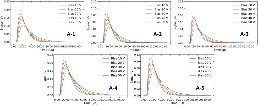
FIGURE 5. Signal waveforms of fabricated PDs in Set A under applied biases from 10 to 50 V for a photon energy of 900 eV.
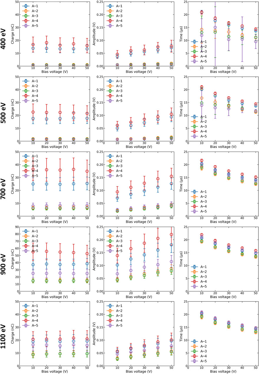
FIGURE 6. Signal charge, amplitude, and time of Set A at photon energies of 400, 500, 700, 900, and 1,100 eV.
The PD charges were normalized to the charges of the EH-GMD photo-electrons using Eq. (1) for each experimental parameter. Considering that the PDs were always saturated at high incident flux in the correlation plot between the PDs and EH-GMD photo-electron charges, the normalized charges of the PDs were obtained after the cuts were applied. The cuts were determined to be 2.0 × 10⁻⁸ C and 3.0 × 10⁻⁸ C for 400 eV and the other energies, respectively. Figure 7 shows the normalized charge distributions as a function of bias voltages for each PD and photon energy, with and without cuts applied. For A-1 and A-4, particularly at a photon energy of 900 eV, which had the highest intensity, the signal charges of the PDs were sufficiently large to be saturated. Thus, the normalized charges significantly increased after the cuts were applied. The detection efficiency of A-4 improved by 55.4% (36.6%) over that of A-1 at 900 eV (on average for all the photon energies). The large errors of 1,100 eV shown in Figure 7 were due to the poor signal-to-noise ratio of the EH-GMD signal. To address this challenge, the gain of the EH-GMD was increased at 1,100 eV for Set B.
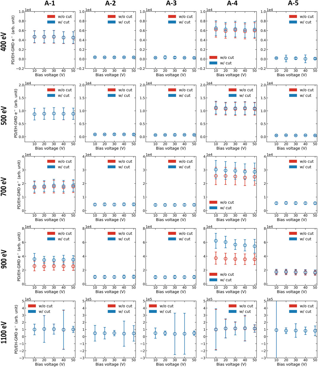
FIGURE 7. Normalized charge distributions as a function of applied bias depending on cuts applied, for A-1–A-5 (left to right) and 400–1,100 eV (top to bottom).
To examine the thickness of the Al metal layer, the ratios of the normalized charges,
Figure 8 shows the averaged signal waveforms of Set B. B-1, B-2 and B-3, which used their P-side for light entrance, had similar sharp rising shape of waveforms. Because B-3 used its N-side for reading the signals, the waveforms were inverted. For the same reason, B-4 and B-5, which used their N-side for light entrance, showed the similar gradual rising shape of waveforms with an opposite sign. B-1, B-2, and B-4 read signals from the P-side, similar to Set A, and B-4 had the same light incident direction as Set A. Thus, their behavior as a function of bias voltages was similar to Set A; increased heights and shorter rising times were observed with an increase in the bias voltage (Figure 9). B-3 and B-5 used their N-side to read the signals; therefore, their waveforms were inverted. Additionally, the waveforms of B-3 and B-5 appeared unaffected by changes in the bias voltage, resulting in minimal change in amplitude and rising time across all the photon energies (Figure 9). Technology CAD (TCAD) simulation [17] was performed to understand the difference in the signal readouts of the P- and N-sides. The simulation revealed that the electric field on the P-side increased and the depletion depth expanded as the bias voltage increased while the electric field on the N-side remained constant (Figure 10). This explains why the N-side signal readout exhibited different waveform characteristics, in terms of the amplitudes, and rising time, compared with the P-side signal readout.
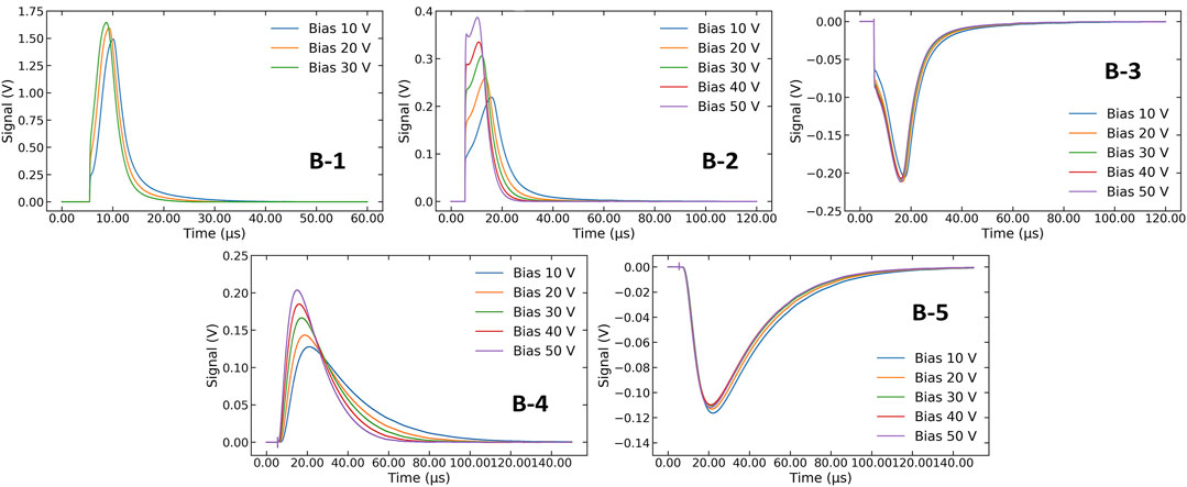
FIGURE 8. Signal waveforms of the HPK-PD (B-1) and fabricated PDs (B-2–B-5) with applied biases from 10 to 30 V or 50 V at 900 eV.
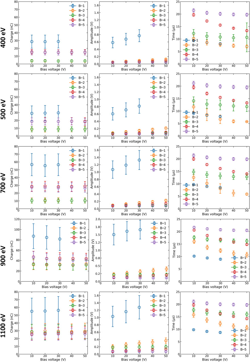
FIGURE 9. Signal charge, amplitude, and time of Set B at photon energies of 400, 500, 700, 900, and 1,100 eV.
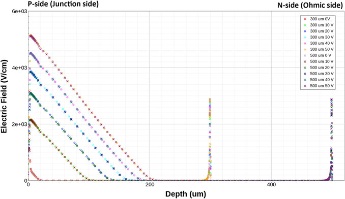
FIGURE 10. TCAD simulation results of the electric field distribution of PDs with thicknesses of 300 and 500 μm.
Among Set B PDs, B-1 had the highest charges and amplitudes at all photon energies. The rising times of B-2 were close to or shorter than those of B-1 at photon energies below 700 eV, which were results of the same cause for the shorter rising times of A-2, A-3, and A-5 within the same energy range. A thick SiO2 passivation layer on the P-side significantly attenuated the incident X-ray flux at a lower energy. The charges of B-2 and B-3, which used the P-side for X-ray entrance, were slightly lower than those of B-4 and B-5, which used the N-side for light entrance, except at 1,100 eV. This was consistent with the normalized charge distributions as a function of bias voltage shown in Figure 11. The effect of the SiO2 was investigated by comparing the ratios of normalized charges
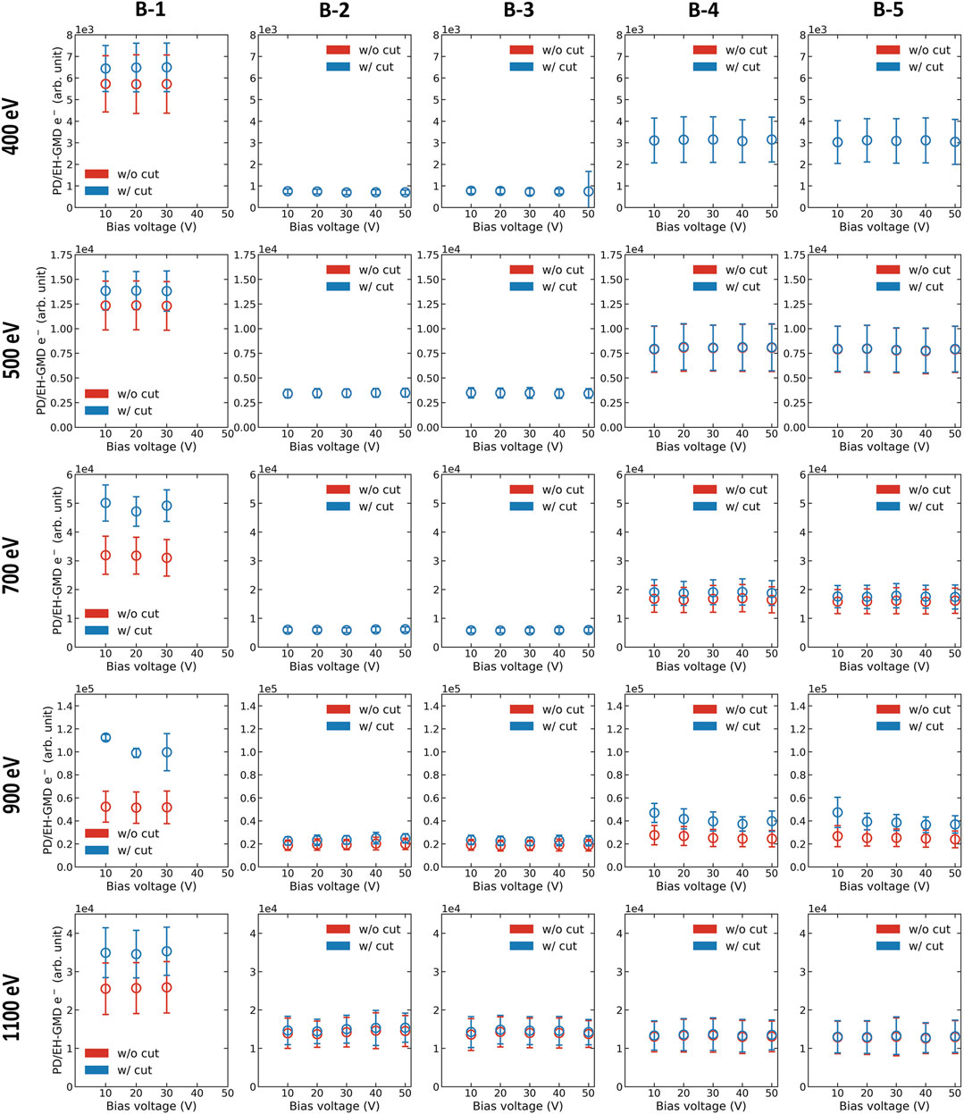
FIGURE 11. Normalized charge distributions as a function of applied bias depending on whether cuts were applied or not, for B-1–B-5 (left to right) and 400–1,100 eV (top to bottom).
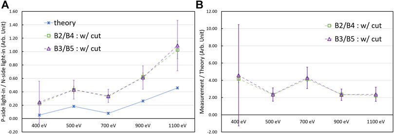
FIGURE 12. (A) Ratios of normalized charge of B-2 (B-3) to that of B-4 (B-5) after cuts were applied and the theoretical values as a function of photon energy. (B) Ratios of the measured to the theoretical values as a function of photon energy with cut.
To compare the fabricated PD with commercial PD, we calculated the ratios of normalized charges
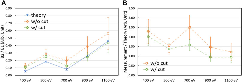
FIGURE 13. (A) Ratios of normalized charge of B-2 to that of B-1 and the theoretical values as a function of photon energy. (B) Ratios of the measured to the theoretical values as a function of photon energy, depending on whether cuts were applied or not.
B-2 and B-4 had a higher amplitude and shorter rising time than B-3 and B-5, respectively. This implied that reading signals from the P-side was appropriate when fast reading was required in case of partial depletion. At 900 eV, the rising times of B-1 to B-5 at maximum bias voltage were 8.9 ± 0.3, 10.7 ± 1.0, 16.2 ± 0.8, 14.8 ± 0.4, and 20.5 ± 0.5 μs, respectively. B-1 and B-2, which used the P-side for light-in and signal-out, had the best rising times, and B-2 was comparable to B-1.
The incident flux was adjusted to three by changing the sizes of the entrance slit and vertical exit slit at a photon energy of 900 eV. At the standard slit setting, all the Set B PDs exhibited different normalized charge distributions depending on whether or not cuts were applied (Figure 11), although there were differences between the PDs. The difference between the normalized charge distributions depending on the existence of cuts for each PD decreased as the incident flux decreased with smaller slit sizes. It was within 1σ for B-1 and disappeared for B-2 to B-5 at the smallest incident flux.
We designed and fabricated PDs for use as diagnostic devices at the PAL-XFEL for detecting X-rays or optical lasers. The PDs were manufactured with different Al metal thicknesses and ARC layers to evaluate the feasibility of fabricating thin metal PDs and assess their functionalities. The electrical characteristics, leakage current and capacitance, of the fabricated PDs were measured, and nine PDs with good electrical characteristics were selected for X-ray beam testing. The X-ray beam test was performed at the soft X-ray beamline of the PAL-XFEL with photon energies ranging from 400 to 1,100 eV. The under-bias voltages were applied to the PDs, and the PD charges obtained integrating waveforms were normalized using EH-GMD charges. Due to saturation observed in the PDs when exposed to unattenuated strong X-ray pulses, the normalized charges were compared after applying cuts to the data. The five PDs with different Al metal thickness and the presence or absence of ARC layers on their N-side were initially tested to evaluate the effect of the metal and ARC layers. The temporal and amplitude characteristics of signal waveforms were modulated by the bias voltage while maintaining a constant normalized charge. The PDs with ARC layers exhibited the better detection efficiency, and particularly the PD with only ARC layer, indicating that the ARC reduced reflection at the silicon surface, even for X-rays. When the ARC and metal layers were present, the anti-reflection effect was evident at photon energies above 700 eV and minimal at the low energy of 500 eV. The estimated transmissions by the metal layers were 1–4 times lower than the theoretical predictions, and this discrepancy widened as the photon energy decreased. These could have been due to the thickness of the TiW layer exceeding the target thickness, unexpected additional layers stacked during other fabrication processes, or reflections at the interfaces of the metal and silicon layers. To investigate the effect of light entrance and signal readout side configurations and compare with a commercial PD, we assembled PDs onto the PCB in four distinct arrangements. The signal waveforms exhibited varying behavior depending on the signal readout side. For the P-side signal-out configurations, the signal waveforms were affected by the bias voltage, as the increasing bias voltage resulted in an enhanced electric field and expanded depletion depth from the P-side. The charge discrepancies between the N-side light-in and the P-side light-in configurations were examined, taking into account the 1,350 nm-thick SiO2 passivation layer on the P-side. Interestingly, the SiO2 layer appeared to serve not only as an attenuating layer but also as an anti-reflection layer, similar to the Si3N4 ARC layer. The P-side light-in and signal-out PD exhibited rapid signal rise times, comparable to the commercial PD which was achieved the highest charge and amplitude values across all photon energies. Accounting for the thick passivation layer of the PD, the normalized charge ratios of the commercial PD and the PD were consistent with the theoretical values at 900 and 1,100 eV. Moreover, the use of an optimized SiO2 layer could potentially enhance the performance of the PD below 700 eV, surpassing that of the commercial PD. Based on the beam test results, we will optimize PDs with different metal and ARC layer parameters, and readout types for various detection purposes.
The original contributions presented in the study are included in the article/Supplementary Material, further inquiries can be directed to the corresponding author.
SL: Formal Analysis, Methodology, Writing–original draft, Writing–review and editing. HH: Formal Analysis, Methodology, Project administration, Writing–original draft, Writing–review and editing. JB: Methodology, Writing–review and editing. SH: Methodology, Software, Writing–review and editing. HJ: Methodology, Resources, Writing–review and editing. JK: Methodology, Writing–review and editing. SK: Methodology, Resources, Writing–review and editing. HP: Supervision, Writing–review and editing.
The author(s) declare financial support was received for the research, authorship, and/or publication of this article. This research was supported by the Korean Government MSIT (Grant No. RS-2022-00164805, Accelerator Application Support Project), the National Research Foundation of Korea (NRF) funded by the Ministry of Education (Grant No. 2022R1I1A1A01068225), and the Ministry of Science and ICT (Grant No. 2018R1A6B4023605, RS-2023-00237194). The EDA tool was supported by the IC Design Education Center (IDEC), Korea.
The authors declare that the research was conducted in the absence of any commercial or financial relationships that could be construed as a potential conflict of interest.
All claims expressed in this article are solely those of the authors and do not necessarily represent those of their affiliated organizations, or those of the publisher, the editors and the reviewers. Any product that may be evaluated in this article, or claim that may be made by its manufacturer, is not guaranteed or endorsed by the publisher.
1. Ko IS, Kang HS, Heo H, Kim C, Kim G, Min CK, et al. Construction and commissioning of PAL-XFEL facility. Appl Sci (2017) 7(5):479. doi:10.3390/app7050479
2. Kang H, Min CK, Heo H, Kim C, Yang H, Kim G, et al. Hard X-ray free-electron laser with femtosecondscale timing jitter. Nat Photon (2017) 11:708–13. doi:10.1038/s41566-017-0029-8
3. Kondratenko AM, Saldin EL. Generating of coherent radiation by A relativistic electron beam in an ondulator. Part Accel (1980) 10:207.
4. Bonifacio R, Pellegrini C, Narducci LM. Collective instabilities and high-gain regime in a free electron laser. Opt Commun (1984) 50:373–8. doi:10.1016/0030-4018(84)90105-6
5. Nam I, Min CK, Oh B, Kim G, Na D, Suh YJ, et al. High-brightness self-seeded X-ray free-electron laser covering the 3.5 keV to 14.6 keV range. Nat Photon (2021) 15:435–41. doi:10.1038/s41566-021-00777-z
6. Park J, Eom I, Kang TH, Rah S, Nam KH, Park J, et al. Design of a hard X-ray beamline and end-station for pump and probe experiments at Pohang Accelerator Laboratory X-ray Free Electron Laser facility. Nucl Instrum Methods Phys Res A (2016) 810:74–9. doi:10.1016/j.nima.2015.11.147
7. Park SH, Kim M, Min CK, Eom I, Nam I, Lee HS, et al. PAL-XFEL soft X-ray scientific instruments and X-ray optics: first commissioning results. Rev Sci Instrum (2018) 89(5):055105. doi:10.1063/1.5023557
8. Jang H, Kim HD, Kim M, Park SH, Kwon S, Lee JY, et al. Time-resolved resonant elastic soft x-ray scattering at Pohang Accelerator Laboratory x-ray free electron laser. Rev Sci Instrum (2020) 91(8):083904. doi:10.1063/5.0016414
9. Dong PT, Cheng JX. Pump-probe microscopy: theory, instrumentation, and applications. Spectroscopy (2017) 32:24.
10. FMB OXFORD. Quadrant beam position monitor (2023). Available from: https://fmb-oxford.com/products/detectors-diagnostics/beam-position-monitors/qbpms/ (Accessed October, 2023).
11. Tono K, Kudo T, Yabashi M, Tachibana T, Feng Y, Fritz D, et al. Single-shot beam-position monitor for x-ray free electron laser. Rev Sci Instrum (2011) 82:023108. doi:10.1063/1.3549133
12. Tiedtke K, Sorokin AA, Jastrow U, Juranić P, Kreis S, Gerken N, et al. Absolute pulse energy measurements of soft x-rays at the Linac Coherent Light Source. Opt Express (2014) 22(18):21214. doi:10.1364/oe.22.021214
13. Lee SC, Baek JM, Hwang SM, Hyun HJ, Kim JY, Kim SH, et al. Development of photo-diodes for Pohang-Accelerator-Laboratory X-ray free-electron laser. Nucl Instrum Methods Phys Res A (2023) 1045:167598. doi:10.1016/j.nima.2022.167598
14. Hamamatsu. Hamamatsu Si PIN photo-diode (2023). Available from: https://www.hamamatsu.com/jp/en/product/optical-sensors/photodiodes/si-photodiodes/S3590-09.html (Accessed October, 2023).
15. Baek JM, Hwang SM, Hyun HJ, Jang H, Kim JY, Kim SH, et al. Performance measurements of photodiodes for X-ray detection. IEEE Trans Nucl Sci (2022) 69:1953–9. doi:10.1109/tns.2022.3186481
16. Center for X-Ray Optics. X-Ray interaction with matter of the center for X-ray optics (2023). Available from: https://henke.lbl.gov/optical_constants/ (Accessed October, 2023).
17. Silvaco. TCAD simulation software (2023). Available from: https://silvaco.com/ko/tcad/ (Accessed October, 2023).
Keywords: PIN photo-diode, fabrication, metal thickness, anti-reflective coating, signal readout, X-ray beam test, Pohang-Accelerator-Laboratory X-ray free-electron laser (PAL-XFEL)
Citation: Lee SC, Hyun HJ, Baek JM, Hwang SM, Jang H, Kim JY, Kim SH and Park H (2024) X-ray beam test of fabricated photo-diodes for Pohang-Accelerator-Laboratory X-ray free-electron laser. Front. Phys. 11:1328639. doi: 10.3389/fphy.2023.1328639
Received: 27 October 2023; Accepted: 08 December 2023;
Published: 04 January 2024.
Edited by:
Jiaguo Zhang, Paul Scherrer Institut (PSI), SwitzerlandCopyright © 2024 Lee, Hyun, Baek, Hwang, Jang, Kim, Kim and Park. This is an open-access article distributed under the terms of the Creative Commons Attribution License (CC BY). The use, distribution or reproduction in other forums is permitted, provided the original author(s) and the copyright owner(s) are credited and that the original publication in this journal is cited, in accordance with accepted academic practice. No use, distribution or reproduction is permitted which does not comply with these terms.
*Correspondence: H. J. Hyun, aGpoeXVuQHBvc3RlY2guYWMua3I=
†Present addresses: J. M. Baek, Department of Physics, University of Illinois at Chicago, Chicago, IL, United States
J. Y. Kim, Capacitor Institute of Technology, Sungho electronics, Gyeonggi, South Korea
Disclaimer: All claims expressed in this article are solely those of the authors and do not necessarily represent those of their affiliated organizations, or those of the publisher, the editors and the reviewers. Any product that may be evaluated in this article or claim that may be made by its manufacturer is not guaranteed or endorsed by the publisher.
Research integrity at Frontiers
Learn more about the work of our research integrity team to safeguard the quality of each article we publish.