
95% of researchers rate our articles as excellent or good
Learn more about the work of our research integrity team to safeguard the quality of each article we publish.
Find out more
ORIGINAL RESEARCH article
Front. Phys. , 20 November 2023
Sec. Radiation Detectors and Imaging
Volume 11 - 2023 | https://doi.org/10.3389/fphy.2023.1285379
This article is part of the Research Topic Pushing Frontiers - Imaging For Photon Science View all 19 articles
 Nord Andresen
 Christos Bakalis
 Peter Denes
 Azriel Goldschmidt*
 Ian JohnsonJohn M. JosephArmin Karcher
 Amanda KriegerCraig Tindall
Resonant Inelastic X-ray Scattering (RIXS) is a powerful spectroscopic technique to study quantum properties of materials in the bulk. A novel variant of RIXS, called 2D RIXS, enables concurrent measurement of the scattered X-ray spectrum for a wide range of input energies, improving on the typically low throughput of 1D RIXS. In the soft X-ray domain, 2D RIXS demands an X-ray camera system with small pixels, large area, high quantum efficiency and low noise to limit the false detection rate in long duration exposures. We designed and implemented a 7.5 Megapixel back-illuminated CMOS detector with 5 μm pixels and high quantum efficiency in the 200–1,000 eV X-ray energy range for the QERLIN 2D RIXS spectrometer at the Advanced Light Source. The QERLIN beamline and detector are currently in commissioning. The camera noise from in-situ 3 s long dark exposures is 7e− or less and the leakage current is 6.5 × 10⁻³ e−/(pixel ∙ s). For individual 500 eV X-rays, the expected efficiency is greater than 75% and the false detection rate is ∼1 × 10⁻⁵ per pixel.
Resonant Inelastic X-ray Scattering (RIXS) is a technique useful to study quantum properties of materials in the bulk [1]. In its simplest and most common implementation, a focused monochromatic X-ray beam impinges on the material under study with an energy very near a chosen element’s atomic electronic transition. When an atom of the specific element in the sample absorbs a beam photon and de-excites through the same atomic transition (resonant condition), the emitted outgoing photon can have the same energy as the beam photons (elastic scattering) or slightly smaller energy (inelastic scattering). In the inelastic case, the outgoing X-ray photon spectrum, which is intrinsically sharp because the final state of the emitting system is the ground state of the atom, carries information about the intrinsic excitations of the molecule/material in which the atom is embedded. In a typical RIXS experiment a spectrometer collects a fraction of the outgoing photons and disperses them by energy, with energy resolving gratings, and a camera captures the image at the end of a long free-flight spectrometer arm to measure the photon-out spectrum.
The cross section for resonant inelastic scattering is small and so is the typical angular acceptance of the spectrometers’ optics due to the mirrors’ dimensions. The dispersing gratings have less than 5% efficiency. These three factors make RIXS, comparatively, a photon-starved technique. Bright light sources, such as synchrotrons and free electron lasers, along with optimized optics designs and efficient X-ray detectors help mitigate this limitation. Still, typical RIXS experiments require exposure times of tens of minutes to obtain a spectrum for a single beam energy value and many such spectra, captured at varying beam energies, are required to produce a full RIXS map.
The novel 2D RIXS concept [2] further addresses the throughput of RIXS. In this variant of RIXS the input X-ray beam is broad spectrum in order to measure the full range of input energies of interest simultaneously. An optical element disperses the input X-ray beam by energy in one dimension (e.g., y). This results in an illuminated segment of a line on the sample such that adjacent points have slightly different X-ray energy photons impinging on them. Like in normal 1D RIXS, optical elements, in this case elliptic and hyperbolic mirrors, focus a fraction of the outgoing scattered X-rays and a grating disperses them in the orthogonal dimension (e.g., x) by their outgoing energy. The mirrors and gratings are arranged such that the 2D pixelated camera at the focal plane measures the full RIXS map. The x-dimension of the image encodes the scattered, outgoing, photon energy while the y-dimension encodes the incoming photon energy. Figure 1 shows the 2D RIXS beam/spectrometer/detection scheme.
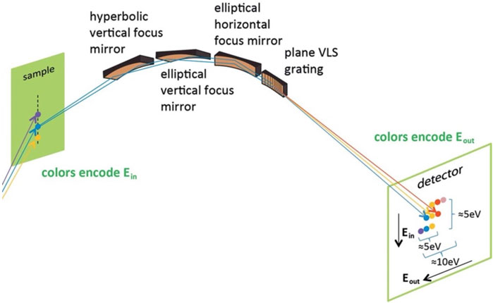
FIGURE 1. 2D RIXS spectrometer scheme. Reproduced with permission from the Journal of Synchrotron Radiation. The monochromator that disperses the incoming photon energies before impinging on the sample is not shown. An (x,y) point on the detector image encodes the impinging X-ray energy (y-coordinate) and the scattered X-ray energy (x-coordinate), thus providing a full RIXS map in one exposure [3].
The concept of 2D RIXS led to the design of the new QERLIN [3] beamline at the Advanced Light Source (ALS) with a RIXS spectrometer. The space-constrained 4.5 m photon flight path length, the targeted spectrometer resolving power of λ/Δλ = 30,000, and the 5–10 eV range of in/out photon energies around the atomic excitation level, constrain the requirements for key dimensions of the camera sensor. In particular, the sensor pixel needs to be 5 μm or less. Furthermore, the requirements of a high quantum efficiency in the 200–1000 eV X-ray energies of interest and of the ability to detect individual X-rays with a fake rate (false positives) negligible with respect to the RIXS signal level constrain the sensor technology, sensor post-processing, temperature of operation and electronic readout noise.
Because of the lack of commercially available cameras that could fulfill all the requirements at the time when the QERLIN system was developed, the design of the custom QERLIN sensor and camera was co-designed with the QERLIN beamline and the spectrometer. Very recently, cameras with similar specification have become commercially available [4].
In this paper, we describe the QERLIN camera system, including the custom built sensor, readout electronics, camera/sensor cooling, mechanical and vacuum components, data acquisition, and image post-processing. We show the camera performance in bench-top testing, including dark images and 5.9 keV soft X-rays response and sensitivity results from a dedicated measurement at the ALS metrology beamline with 500 and 900 eV X-rays.
At the time of this writing, the QERLIN spectrometer is being commissioned and the camera has not yet seen first spectrometer light. We show, however, the camera performance in dark images as installed at the end of the spectrometer and measure the expected fake rate as a function of X-ray energy based on the real dark images and on the expected and partly characterized X-ray signal response.
The QERLIN sensor consists of a 2,048 rows by 3,840 columns array of 5 μm × 5 μm pixels that satisfies the spectrometer resolving power requirements and in and out energy ranges given the 4.5 m long QERLIN spectrometer arm and its optics. It is a thinned back-illuminated CMOS Active Pixel Sensor with a 4T architecture [5]. As such, there are 4 transistors per pixel. Charge is collected in a pinned photodiode structure in the pixel. A transfer gate moves the charge to the output node (also referred to as the floating diffusion) which is previously cleared by means of a reset transistor. A third transistor, in a source-follower configuration, outputs a voltage proportional to the collected charge. The fourth transistor, in a switch configuration, selects the pixel for readout.
The QERLIN sensor is segmented into 16 regions of 2048 (rows) by 240 (columns) pixels, where each region has an independent analog output. The fourth in-pixel transistor selects the row, while a multiplexer at the bottom of the columns selects the column to be presented at the analog output for each channel. Externally provided signals control in-chip logic that can a) turn on the transfer gate transistors for all the pixels or only for the selected row b) reset the floating diffusions for all the pixels or only for the selected row c) select the next row d) select the next column and e) reset the digital logic to select the first row and first column of each channel. The sensor logic supports both global shutter and rolling shutter operation, the latter by resetting the previous row’s pixels automatically.
Besides digital power, the sensor requires externally supplied DC voltages, 1.8 V and 3.3 V, and bias currents for its operation: a reset voltage, a pixel source follower voltage, rails for the transfer gate and for the reset transistor gate, along with a voltage and two currents for the bottom-of-column circuitry and a voltage for the output stage.
The QERLIN sensor has 16 analog outputs along the bottom edge of the chip. Voltage supplies to power the bottom-of-column (BOC) and for the output stage are also along the bottom side along with bias currents for the BOC analog circuitry. On the top side there are pads to supply the voltage for the sensor columns and the voltage for pixel reset. On the left side are pads for LVDS clocks and for other LVDS digital signals that control sensor timing and reset/exposure/readout sequencing.
Fabrication of the sensor was done using a UMC 180 nm CMOS image sensor process. The starting material is a p-type silicon substrate with a moderate resistivity (with type p-) epitaxial (EPI) layer. The EPI layer, which functions as the sensitive volume of the sensor, is 4 μm thick.
Soft X-rays in the 200–1,000 eV have attenuation lengths in silicon from 63 nm to 2.7 μm. The passivation, metal and oxide layers on the transistor-implanted/patterned side of the sensor are several micrometers thick. Thus, illumination from the non-patterned side, often referred to as back-illumination, is required for efficient detection of X-rays in this energy range. Furthermore, the silicon substrate material, where charge carriers readily recombine, needs to be removed. This process, referred to as thinning, exposes the sensitive EPI layer to the X-ray illumination.
In order to maintain the sensor’s mechanical rigidity, only the imaging area of the QERLIN sensor was thinned to the EPI (by an outside vendor) after dicing, leaving a full thickness frame around it. The picture in Figure 2 shows the back side of the fully post-processed QERLIN sensor.
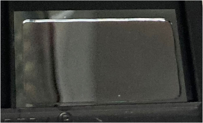
FIGURE 2. Picture of back side of the thinned QERLIN sensor. A full thickness frame is left for rigidity and ease of handling.
The etched surface of the thinned sensor has a relatively high number of microscopic defects left over from the etching process. These defects produce an unacceptable level of thermally generated leakage current. Therefore a high quality, p-type layer on the entrance side of the device is needed to isolate these defects from the electric field of the device and prevent them from injecting current into the active volume of the detector. No explicit contact to ground of the back surface is made but the conductive implanted layer is effectively grounded on the edges of the sensor.
Since thinned devices cannot be further processed at the foundry, it is necessary to have a contact fabrication process that can be performed on fully metallized chips. This means that the maximum processing temperature that can be used has to be low enough to avoid damaging the aluminum metallization and the interlevel dielectric layers (ILD). Temperatures that are too high can alloy the metal with the underlying silicon or crack the ILD, either of which will destroy the chip. The exact temperature at which this happens is highly dependent on the particular foundry process used to make the sensor.
For the QERLIN sensor, we chose to use a process that we have developed to fabricate contacts at low temperatures. This process uses ion implantation followed by annealing to electrically activate the dopant. This process produces high quality contacts that are ∼100 nm thick. Contacts fabricated using this method effectively suppress the leakage current to a level that is acceptable for this application.
We have developed an additional contact fabrication process based on molecular beam epitaxy (MBE) that produces high quality contacts of 10 nm thickness or less. With such thin contacts the efficiency at the low end of the soft X-ray energy range can be increased four-fold. For instance, for 200 eV X-rays the attenuation length in silicon is 63 nm and the 10 nm dead layer absorbs a very small fraction of the photons. We plan to replace the sensor in the QERLIN camera with an MBE contact device in the near future.
Even in a thinned detector, leakage current is significant at room temperatures. Therefore, cooling the sensor is important. Cooling, in turn, enables the long exposure times useful in a soft X-ray spectrometer due to its low photon flux. In addition, long exposure times (without saturation from X-ray signal or from dark current) are desirable in order to increase the signal level with a fixed readout noise contribution.
The thermal design has two main requirements: to cool the sensor to a stable temperature between −20°C and −50°C and to prevent the overheating (<60°C) of the in-vacuum electronics (pre-amps, etc.). The sensor is glued to a silicon carbide (SiC) thermal-bus with a thin film of thermally conducting epoxy around the non-thinned frame of the sensor. Besides being a good thermal conductor, SiC has a similar coefficient of thermal expansion to the silicon sensor. The cold sides of the two three-stage solid-state thermoelectric coolers (TECs) are glued to the SiC thermal-bus with thermally conductive epoxy. The hot surface of the TECs is likewise glued to a thick copper plate. When operating at full power, the TECs dissipate about 45 W each and are the main thermal load on the system. The picture in Figure 3 shows the sensor/SiC/TECs/thick-copper-plate assembly. The picture shows the side of the sensor where the wire bonds are made, while the X-rays impinge from the bottom thinned-side. Two PT-100 thermistors monitor the SiC/sensor cold temperature and the thick-copper-plate (near room) temperature. The wires to power the TECs and to measure the PT-100 resistances come out of the vacuum enclosure through a dedicated 9-pin feedthrough.
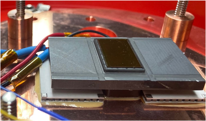
FIGURE 3. The internal thermal/mechanical assembly: The 1.2 cm × 2.0 cm QERLIN sensor is in the center (soft X-rays entrance is from the bottom of the image -the thinned back side of the sensor-), glued to a SiC which in turn is glued to the cold-end of 2 TECs.
The in-vacuum electronics board is a flex-circuit board with discrete components for pre-amplifiers, current sources, and voltage sources for the sensor operation. The flex-circuit board is glued to a backing of thin copper sheet. This sheet is mechanically attached and thus thermally coupled to the externally cooled thick-copper-plate. A thin Vespel frame around the sensor thermally isolates the flex-circuit board from the SiC to minimize the heat load on the TEC’s cold-side. Figure 4 shows the in-vacuum assembly right before wire-bonding of the sensor.
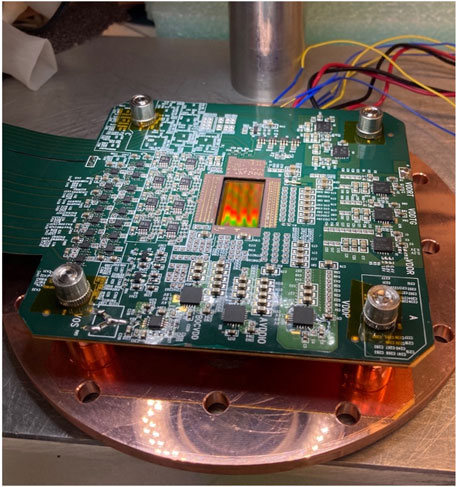
FIGURE 4. In-vacuum electronics. While the sensor is operated at −50°C, the in-vacuum electronics is thermally isolated from the cold side of the TECs and is kept near room temperature.
The thick-copper-plate with the sensor assembly is sandwiched between a clamping ring and the aluminum-body which, in turn, is mated to a 2.5″ Conflat flange at the center of the main 8″ camera vacuum flange. The aluminum-body accepts, from the air-side, a tightly fitting stainless steel cold-probe. Coolant flows through the internal manifold of this cold-probe to facilitate the room-temperature cooling circuit. The nearly 100 W of power dissipated in-vacuum is thus removed by the coolant loop of the cold-probe and maintains the temperature of the thick-copper-plate and electronics to less than 40°C and the QERLIN sensor (via the TECs) near −50°C. Figure 5 shows the design of the thermal components around the sensor and the in-vacuum electronics and Figure 6 shows the fully assembled QERLIN camera mounted on the main 8” flange. The rectangular cutout in the thick-copper-plate is the entrance window for the X-rays from the spectrometer to the back-side of the sensor. The sensor is recessed with respect to the copper plate but this has no impact on the camera X-ray acceptance because the incident rays are nearly perpendicular to the sensor. The two circular openings, adjacent to the entrance-window, contain reed-valves (movable flaps of polyamide film). These reed-valves prevent a large pressure differential (during system pump-down, venting and vacuum failures) between the backside and the front-side of the highly fragile thinned sensor. The sensor and reed-valves act as a vacuum barrier to isolate the non-VHV (very-high-vacuum), internal camera components operating at high-vacuum from the main system operating at VHV.
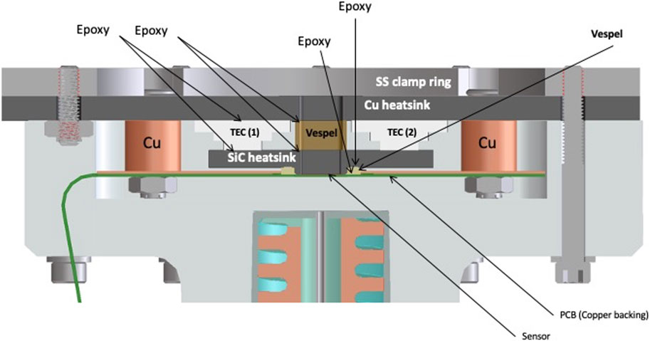
FIGURE 5. Details of the thermo-mechanical design of the QERLIN camera. X-rays come from the top side and the layers before the sensor have cut-outs.
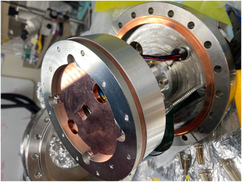
FIGURE 6. Flange-mounted in-vacuum components of the QERLIN camera. The rectangular opening in the copper plate is the entrance port for the X-rays.
The camera readout hardware is organized as follows: 1) the in-vacuum flex board that connects to the main flange vacuum feedthroughs with two 51-pin connectors, 2) an in-air electronics box that connects to the air-side of those feedthroughs and delivers digital data through an optical fiber and 3) a Linux server that receives the digital data via a 10 GigE optical fiber network.
The in-vacuum flex board has single-ended preamplifiers and single-ended-to-differential amplifiers for the 16 analog output channels of the QERLIN sensor. The 16 differential analog outputs come out through one of the 51-pin feedthroughs. A single adjustable voltage controls the offset level of all the sixteen channels. Linear regulators on the board provide the DC voltages required for the sensor operation. Three current mirror circuits provide the DC currents needed and are powered with regulated voltages. All digital control signals and clocks come through one of the feedthrough interfaces as LVDS pairs. On the board, some of the signals (e.g., two non-overlapping clocks) are just passed through to the sensor, while others are converted to single-ended signals (like the global reset) as required by the sensor design.
The in-air electronics box has a simple pass-through motherboard, a power board, a transfer gate pulser board and the main DAQ board (ADAQ). This ADAQ board has 16 channels of differential amplifiers, 4xQuad ADS5263 16-bit ADC chips capable of 100 mega-sample per second per channel, an Enclustra KX1-325 FPGA module and two 10GigE network interfaces. The custom FPGA code orchestrates the sensor signaling, through a set of 16 LVDS signals, and the output digitization. It organizes the digital output as full physical image frames. It presents the organized digitized data through the 10GigE network interface as UDP packages. Control of the FPGA DAQ cycle is through a set of about 30 control registers that are accessible from the Linux server through a dedicated network port opened by the FPGA on the 10GigE connection.
The QERLIN sensor supports both global shutter and rolling shutter readout modes. In addition, the device provides a large degree of operational flexibility because most of its control signals are externally supplied. As discussed above, the 2D RIXS application benefits from as low a noise figure as possible and the required and desirable frame rate is from slow O(Hz) to very slow O (mHz). In what follows we describe the default readout cycle for the QERLIN camera with rolling shutter with pause, sample/reset averaging and correlated double sampling. This readout cycle was used to take the characterization data presented in the next sections. Figure 7 shows a simplified timing diagram of the readout sequence.
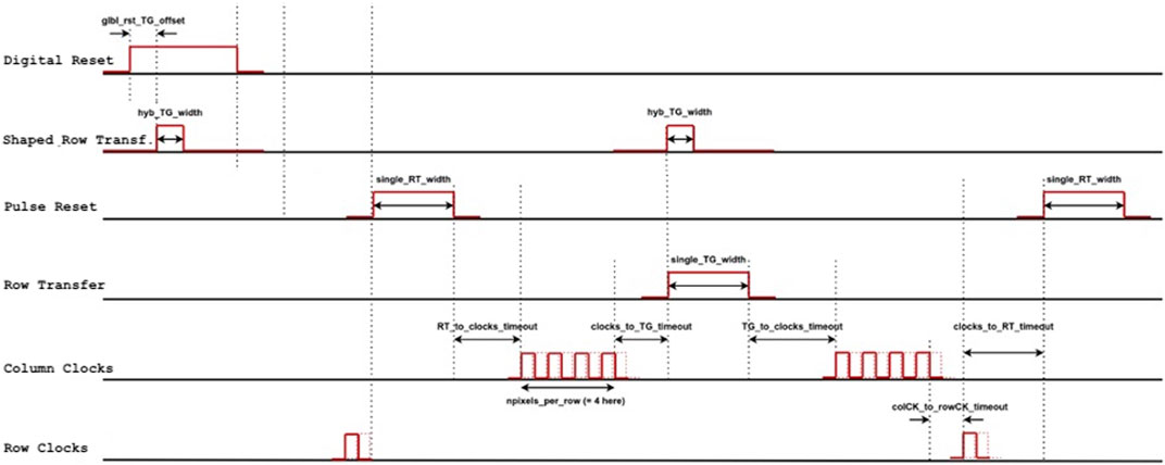
FIGURE 7. Simplified timing diagram of the default readout sequence.
A Digital Reset signal prepares the device for selection of the first physical row of pixels. Then a Row Clock signal selects the next (first) row. A Pulse Reset signal then resets the voltage on the output node (floating diffusion) of all the pixels in that row. A Column Clock signal then selects the next (first) column in the channel (or super-column). Eight consecutive ADC samples (for the same reset pixel) are acquired to be averaged in the FPGA to reduce the readout thermal noise component. A new Column Clock signal then selects the following column in the super-channel followed by the corresponding 8-sample read. This is repeated until the averaged reset samples from all 240 columns of the channel have been acquired. Next, the charges stored in the pixels’ photodiodes of the selected row are transferred to the output nodes. This is achieved by issuing a Row Transfer signal. After the charge transfer is completed the pixels are read out analogously to the reset read sequence (i.e. 8 ADC samples per pixel that are then averaged). After the readout of the entire row, a new Row Clock signal selects the next row for corresponding reset/signal readout. While the next row is being read out, the previous row is (automatically) fully reset by having its transfer gate on while the reset is issued (thus resetting both the output nodes and the photodiodes). After the last row of the sensor is read out and reset, an arbitrary duration pause of all signals extends the pixels’ integration time to the desired total frame exposure time. At the pause’s end the cycle restarts with a new Digital Reset signal. In this fashion, all the pixels in the sensor have equal (although not fully contemporaneous) exposure time.
The entire cycle takes about 3.2 s when the pause between frames is removed. With the ADCs clocked at 12.5 MHz the ADC sampling (8 + 8 samples per pixel) takes only 0.6 s (80 ns per sample × 240 columns per channel × 2048 rows × 16 samples per pixel). The bulk of the additional time, 2 out of the remaining 2.4 s, is used for the charge transfer operation between the photodiodes and the output nodes which takes 950 μm (for each of the 2,048 rows). Efficient charge transfer can be achieved in 10–100 ns. However, it was found that, in order to obtain the best noise performance, a pulse with a long decay time to turn off the transfer gate is needed. This long and shaped pulse is provided by the transfer gate pulser board in the in-air electronics box. We hypothesize that the additional noise we observe when the transfer gate is abruptly turned off, approximately 20e−, is due to a charge partition effect [6, 7] by which a more or less constant charge from under the switched-on transfer gate can end-up stochastically in the photodiode or the floating diffusion as the transfer gate is switched off.
A multi-threaded data acquisition software program runs on a Linux server. It establishes a private network connection with the in-air electronics through an optical fiber 10 GigE link. At startup it sets up the parameters for the image frames’ acquisitions (readout mode, internal/external trigger, exposure time, duration of the various steps in the readout cycle, base ADC clock speed, etc.) by setting the FPGA registers.
The FPGA logic supports all the readout modes of the sensor. The logic is implemented in a Xilinx/AMD Kintex-7 FPGA that is hosted by the Enclustra KX1-325 board. The FPGA implements a 10G UDP Ethernet interface with the back-end Linux-based server. It also interfaces with the ADS5263 ADCs, and establishes a high-speed link between them upon startup. A dedicated block deserializes the digitized sensor data outputted by the ADCs, and drives them to the back-end 10G Ethernet interface that in turn forwards the data to the DAQ software server. The firmware also supports different readout modes of the sensor, and can also perform an on-the-fly rolling average pre-processing of the data before shipping them to the DAQ server; it can also temporarily store one single image frame to an external RAM module, and then subtract its values from the next one that is acquired, thus performing a correlated double-sampling to remove the reset noise component. A block diagram of the FPGA firmware and its surrounding hardware modules can be viewed in Figure 8.
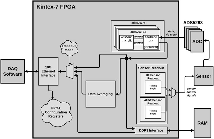
FIGURE 8. FPGA firmware block diagram, depicted alongside its associated peripherals.
In the software side, the main thread of the DAQ program listens for UDP packages from the camera and accumulates entire frames in a memory buffer. Each image frame consists of 2 × 2,048 × 3,840 16-bit (unsigned) samples, or 30MBytes. The rows are interleaved such that an entire row’s reset values (already 8x averaged) is followed by the row’s signal values. Data flow control is achieved by verifying that no consecutive data packet was missed and if packets are missing a software buffer and sensor/FPGA-flow reset is issued. In the default camera operation mode, with one frame every 3.2 s, the data flow rate is less than 100 Mb/s and no network or computer resources are significantly stressed.
Two additional threads move full buffers of frames to disk files for offline analysis and to a ZMQ-protocol network queue for online data monitoring.
The first step of image processing is to de-interleave the Reset and Signal data frames. Next, the correlated double sampling (CDS) image is computed, simply by calculating Signal-Reset for each frame. This step removes per-pixel and per-column readout offsets. It also removes the kTC noise from the opening of the in-pixel reset switch.
The next step is dark subtraction. The CDS images contain contributions from leakage current accumulated in the photodiodes during the exposure (readout time + pause) and from charge injection from the transfer gate operation. A dark data set is used to compute the per-pixel average (over multiple dark frames) of the dark CDS which is then subtracted frame-by-frame from the CDS (non-dark) frames. For data runs where the external illumination is very sparse (such as the 55Fe 5.9 keV X-ray calibration data sets described in the following section) the CDS dark image can be obtained from the illuminated data set by computing the per-pixel median over a set of CDS images. The per-pixel median is a very good approximation to the most-probable-value in these very sparsely illuminated images and is used for convenience.
Measurements of the camera response to 5.9 keV X-rays from a 55Fe source provide information on the conversion factor from ADU (arbitrary digital units) to ionization electrons, on the sensor response uniformity and on the effective point spread function of the camera.
The camera was first pumped to a 1 × 10⁻⁵ torr pressure and then the TECs were turned on to maximum power until a stable temperature of about −50°C was reached. A 12 mCi 55Fe source was placed outside the vacuum enclosure in front of a thin aluminized mylar window a few inches away from the back side of the QERLIN sensor.
In evenly illuminated dark-subtracted CDS frames almost point-like clusters of pixels from individual 5.9 keV X-rays are distributed uniformly over the entire sensor area. Figure 9 shows a random zoomed-in 100 × 100 pixel patch of an image. Typical 5.9 keV X-ray depositions have 1–4 pixels with a significant fraction of the X-ray induced charge depending on the exact location of the X-ray absorption within the pixel. Based on the roughly approximated experimental geometry, the source activity and the estimated X-ray absorption between the source and the sensor surface, the estimated impinging X-ray flux is ∼0.006 X-rays per pixel per second. At this X-ray energy only about 4.5% of those convert in the 2.5 micron thick sensitive volume, therefore, for 3.6 s long exposures we expect 9.5 X-rays detected in a 100 × 100 pixel patch, in reasonable agreement with our observations.
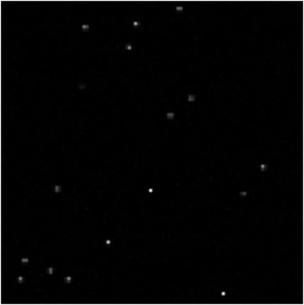
FIGURE 9. A random 100 × 100 pixel patch with several X-rays clusters. The image contrast is set such that the brightest X-ray pixels are white and it is not zero-suppressed.
Figure 10 shows the single pixel value distribution (after CDS and dark subtraction) from many frames. The Gaussian fitted peaks near 3000 ADU are due to “single-pixel” energy depositions from the Kα and Kβ lines of the 55Fe source. Their relative position matches to better than 1% the nominal 5.88 keV 6.49 keV source lines. These single-pixel depositions occur when the X-ray conversion happens in a fully depleted part of the pixel volume under the photodiode implant. The region below the peak in Figure 10 but above the residual noise near zero is due to pixel charge sharing from multi-pixel clusters. A calibration factor of 1.8 ADU/e− was deduced from the measured position of the single-pixel Kα peak and the average deposited energy to produce an e-h pair in silicon WSi = 3.6 eV.
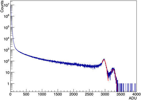
FIGURE 10. Single-pixel-value distribution for dark subtracted CDS images with 55Fe X-rays. The two peaks near 3,000 are due to the two X-ray lines at 5.9 and 6.4 keV from the source. The fitted FWHM of the peaks is 61 e, using the ADU to e− conversion derived from the peaks’ locations.
Since a large fraction of the X-ray hits deposit their charge over multiple pixels we perform a simple cluster analysis. Seed pixels are identified as local maxima with values greater than 3*σn, where σn is the standard deviation of the pixel values in dark images. For each seed pixel the sum of the pixel values in the 3 × 3 region around the seed is computed. Figure 11 shows the distribution of the 3 × 3 cluster charge (now in a linear plot). The peaks near 3,000 and 3,300 are from 3 × 3 clusters seeded on “single-pixel” depositions. The broader and much larger peak near 2,500 is from clusters with shared charge. For these the charge collection is incomplete, leaving about 15% of the charge unaccounted for. Larger cluster regions (5 × 5, 7 × 7) do not recover the missing charge. On the other hand, the spectrum of the 3 × 3 integrated signal is, as expected, much cleaner with far fewer entries between the noise peak and the iron peaks than the “single-pixel” distribution of Figure 10.
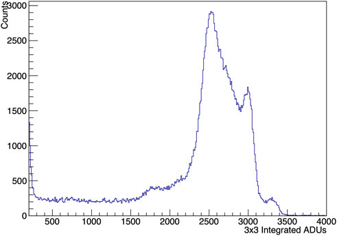
FIGURE 11. Distribution of the signal sum over 3 × 3 pixel clusters.
In order to study the camera response uniformity (excluding quantum efficiency effects), we select all clusters with a 3 × 3 integrated signal in a broad window around the peak (between 2,000 and 3,500 ADU). We re-bin the sensor area into patches of 16 × 24 pixels (to ensure enough statistics in each bin) and calculate the average value of the cluster charges. Figure 12 shows the sensor response to 5.9 keV X-rays. Within the statistical limit of the measurement the response is uniform. The dark corners are the result of the absence of clusters in those regions because the thinning process reached a slightly undersized region and the 5.9 keV X-rays are fully absorbed in the thick substrate of the un-thinned frame.
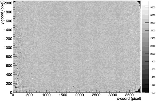
FIGURE 12. QERLIN camera response uniformity. The mean response is 2,650 ADU per X-ray and the RMS is 108 ADU. This corresponds to a 4% response uniformity (without any corrections to the data).
We took dark data using the standard detector configuration (e.g., −50°C and 3.2 s/frame) with the QERLIN detector installed at the end of the QERLIN spectrometer arm at the ALS. Figure 13 shows the residuals from the median subtracted CDS dark images. The central component of the residuals distribution is well fitted to a Gaussian (in the [−30,30] range) with 11.6 ADU sigma. Using the conversion factor from the X-ray data this corresponds to 6.5 e− noise. There is, however, a clear non-Gaussian tail to the noise residuals. We fit these noise tails in the [100, 300] range to a single exponential. Noise tails can be due to hot pixels with excess leakage current or other electronics effects. A correlation study between the dark current images (see next section) and noise images showed only a 0.13 correlation (where 0 is no correlation and 1 is full correlation) between those. This indicates that the bulk of the noise tail is not due to high leakage hot pixels.
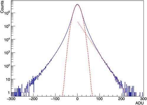
FIGURE 13. Noise residuals from a dark run (−50°C and 3.2 s exposure time).
Two dark data sets with per-frame exposure times of 50 s and 1,000 s were utilized to determine the dark current in standard operating conditions (−50°C). For each data set we compute the (per-pixel) median of the set of CDS frames. We then subtract pixel-by-pixel the median image of the 50 s exposure from the median image of the 1,000 s exposure. Figure 14 shows the pixel value distribution of the difference image. The distribution has a mean of 11.2 ADU. Accounting for the additional exposure time this corresponds to 6.5 × 10⁻³ e/(pixel ∙ s). This very low leakage component enables long up to 1,000 s exposure times without significantly increasing the overall noise. The distribution has a tail on the positive side due to ∼0.1% of all pixels that have higher dark current.
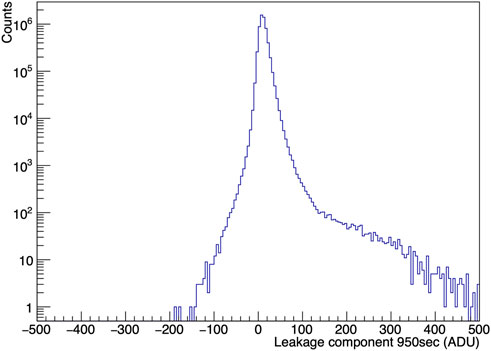
FIGURE 14. Raw dark current signal contribution from 950 s supplementary exposure. It corresponds to a very low 6.5 × 10⁻³ e−/(pixel ∙ s) leakage.
As described in the introduction, in the 2D RIXS application a point in the image corresponds to an energy-in energy-out pair. Some regions of 2D RIXS images may have very low photon flux but still carry important information. For this reason, it is important to have a fake hit rate negligible compared to the RIXS signal. A fake hit is the measurement of localized pixel values consistent with the signal expected from an individual X-ray detection in a region where no X-ray hit.
We estimate the expected fake hit rate using the dark data runs and the expected soft X-ray signal. To estimate the expected signal from 200–1,000 eV soft X-rays we use the measured detector response to individual 5.9 keV 55Fe X-rays and linearly scale the charge depositions by the X-ray energy. To find fake hits in the dark data set we use a two-threshold method. The first threshold requires that a local pixel maximum is greater than 3σ (like before, σ is obtained from the fit to the [−30,30] region of the noise residuals). For each local maximum, the sum of the four largest pixel values within a 3 × 3 pixel region around the maximum is calculated (q4). The second threshold is on the value of q4. The q4 threshold is scanned to compute, for each q4 threshold value, the fake hit rate from the noise images and the soft X-ray detection efficiency from the scaled 55Fe response. Figure 15 shows the calculated single X-ray detection efficiency versus the corresponding measured fake hit rate (the number of fake hits per image) as the q4 is varied and for multiple soft X-ray energies of relevance in RIXS. For example, for individual 500 eV X-rays, one can choose a threshold for which the expected efficiency is greater than 75% and the false detection rate is ∼1 × 10⁻⁵ per pixel.
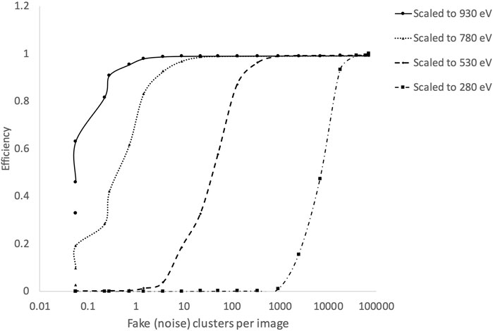
FIGURE 15. Calculated X-ray cluster detection efficiency vs. measured fake hit rate per image for various typical soft X-ray energies used in RIXS experiments. The tradeoff is controlled with a threshold on q4 (see text). The efficiency calculation assumes a fully efficient (like from an MBE) back contact.
This calculation assumes no significant inefficiency from the absorption of X-rays in the thin dead layer on the illuminated back-side of the sensor. For 530 eV X-rays on a dead silicon layer of 120 nm this reduces the efficiency by 22%, while the reduction is 65% at 280 eV and just 5% at 930 eV. A future version of the sensor with an MBE contact dead layer of less than 10 nm should show efficiencies similar to those plotted.
To understand the effect of the expected fake hit rate, it is useful to look at an example. Take the hardest case of 280 eV X-rays (a sensor with an MBE contact is assumed): for a suitably chosen threshold we expect >80% quantum efficiency and an estimated 10,000 fake hits per image (see Figure 15), randomly and uniformly distributed. On the other hand, the “true” signal component over the entire image would have millions to 100s of millions of X-ray hits. Thus the fake hits represent a small contribution, between 0.01% and 1%. Additionally, in 2D RIXS maps produced from series of 1D RIXS spectra, the typical features span contiguous regions of many pixels, typically 100s. As a consequence, the spatially uncorrelated fake hits have the effect of marginally reducing the overall signal-to-noise of those multi-pixel features by adding a dim and spatially flat component.
While most of the detector characterization was obtained from dark images and 55Fe X-rays, the QERLIN camera was also installed and briefly tested at the ALS 6.3.2 metrology beamline. Unfortunately, the geometry of the setup was constrained and the beam illuminated an area at the sensor’s edge, with partial coverage. Given those circumstances, no reliable quantum efficiency measurement could be obtained from that data. However, selecting the part of the images with a much dimmer beam halo we could identify and measure individual well-isolated X-rays at the two beam energies we used, 500 and 900 eV. From those, we verified the camera response linearity to ∼10% in the 500 eV–5.9 keV range.
At the time of this writing, the 2D RIXS QERLIN beam line and spectrometer at ALS are being commissioned. The QERLIN camera described in this article is installed and operational at the spectrometer. The camera data acquisition is fully integrated with the beam line and spectrometer controls. We demonstrated the camera performance in dark images as installed and measured the expected fake rate as a function of X-ray energy based on the real dark images and the expected and partly characterized X-ray signal response.
The raw data supporting the conclusion of this article will be made available by the authors, without undue reservation.
NA: Conceptualization, Investigation, Writing–review and editing. CB: Methodology, Software, Writing–review and editing. PD: Conceptualization, Funding acquisition, Investigation, Methodology, Project administration, Supervision, Writing–review and editing. AG: Data curation, Formal Analysis, Investigation, Methodology, Software, Validation, Visualization, Writing–original draft. IJ: Methodology, Software, Writing–review and editing. JJ: Conceptualization, Funding acquisition, Project administration, Resources, Supervision, Writing–review and editing. AKa: Investigation, Methodology, Writing–review and editing. AKr: Conceptualization, Investigation, Methodology, Writing–review and editing. CT: Conceptualization, Methodology, Writing–review and editing.
The author(s) declare financial support was received for the research, authorship, and/or publication of this article. This work was funded by the Advanced Light Source and by the U.S. Department of Energy, Office of Basic Energy Sciences, Scientific User Facilities Division, through grants from the Accelerator and Detector Research Program. Work was performed at the Lawrence Berkeley National Laboratory, which is supported by the U.S. Department of Energy under contract no. DE-AC02-05CH11231.
We thank Yi-De Chuang, Harold Barnard and Alastair McDowell for their help throughout the camera development, installation and commissioning at the ALS QERLIN spectrometer. We thank Martin Keller for his work on the integration of the camera with the beam and spectrometer control and monitoring. Braeden Benedict designed and built the camera temperature controller. Michael Holmes performed finite element analysis of the in-vacuum thermal design. We thank Terry Mcafee and Eric Gullikson for their help with the camera measurements at the ALS 6.3.2 metrology beam line.
The authors declare that the research was conducted in the absence of any commercial or financial relationships that could be construed as a potential conflict of interest.
All claims expressed in this article are solely those of the authors and do not necessarily represent those of their affiliated organizations, or those of the publisher, the editors and the reviewers. Any product that may be evaluated in this article, or claim that may be made by its manufacturer, is not guaranteed or endorsed by the publisher.
1. Ament LJP, van Veenendaal M, Devereaux TP, Hill JP, van den Brink J. Resonant inelastic X-ray scattering studies of elementary excitations. Rev Mod Phys (2011) 83(2):705–67. doi:10.1103/RevModPhys.83.705
2. Strocov VN. Concept of a spectrometer for resonant inelastic X-ray scattering with parallel detection in incoming and outgoing photon energies. J Synchrotron Radiat (2010) 17(1):103–6. doi:10.1107/S0909049509051097
3. Warwick T, Chuang Y, Voronov DL, Padmore HA. A multiplexed high-resolution imaging spectrometer for resonant inelastic soft X-ray scattering spectroscopy. J Synchrotron Radiat (2014) 21(4):736–43. doi:10.1107/S1600577514009692
4. Marana-X sCMOS. Examples of these are the Marana-X sCMOS cameras, with slightly bigger 11 or 6.5 μm pixels and >90% quantum efficiency in the soft X-ray regime along with <2 e- noise and fast readout (2023).
5. Lee P, Gee R, Guidash M, Lee T-H, Fossum ER. An active pixel sensor fabricated using CMOS/CCD process technology, Proceedings of the presented at the IEEE Workshop on Charge-Coupled Devices and Advanced Image Sensors, Dana Point, California, April 1995. 1995.
6. Teranishi N, Mutoh N. Partition noise in CCD signal detection. IEEE Trans Electron Devices (1986) 33(11):1696–701. doi:10.1109/T-ED.1986.22730
Keywords: RIXS, x-ray, CMOS sensor, spectrometer, back-illumination, low noise, synchrotron, light source
Citation: Andresen N, Bakalis C, Denes P, Goldschmidt A, Johnson I, Joseph JM, Karcher A, Krieger A and Tindall C (2023) A low noise CMOS camera system for 2D resonant inelastic soft X-ray scattering. Front. Phys. 11:1285379. doi: 10.3389/fphy.2023.1285379
Received: 29 August 2023; Accepted: 26 October 2023;
Published: 20 November 2023.
Edited by:
Jiaguo Zhang, Paul Scherrer Institut (PSI), SwitzerlandReviewed by:
Andrea Castoldi, Polytechnic University of Milan, ItalyCopyright © 2023 Andresen, Bakalis, Denes, Goldschmidt, Johnson, Joseph, Karcher, Krieger and Tindall. This is an open-access article distributed under the terms of the Creative Commons Attribution License (CC BY). The use, distribution or reproduction in other forums is permitted, provided the original author(s) and the copyright owner(s) are credited and that the original publication in this journal is cited, in accordance with accepted academic practice. No use, distribution or reproduction is permitted which does not comply with these terms.
*Correspondence: Azriel Goldschmidt, YWdvbGRzY2htaWR0QGxibC5nb3Y=
Disclaimer: All claims expressed in this article are solely those of the authors and do not necessarily represent those of their affiliated organizations, or those of the publisher, the editors and the reviewers. Any product that may be evaluated in this article or claim that may be made by its manufacturer is not guaranteed or endorsed by the publisher.
Research integrity at Frontiers
Learn more about the work of our research integrity team to safeguard the quality of each article we publish.