 Edwin Sebastian Barrera-Mendivelso
 Arturo Rodríguez-Gómez
- Instituto de Física, Universidad Nacional Autónoma de México, Ciudad de México, Mexico
Silicon nitride’s excellent electronic and optical properties have positioned it as an indispensable element in silicon-based photonic platforms and photonic quantum computing. Chemical Vapor Deposition (CVD) and Plasma Enhanced CVD (PECVD) techniques predominate in high-performance silicon nitride thin film manufacture. Unfortunately, Chemical Vapor Deposition and Plasma Enhanced CVD are expensive techniques that use hazardous gases and very high substrate temperatures. In this work, we used the sputtering technique to grow α-Si3N4 thin films at room temperature. We identified that by applying radiofrequency powers between 30 and 50 W combined with deposition times below 120 min, we could achieve the growth of silicon nitride (SiNX) films with uniformly distributed crystalline particles, limited formation of clusters, and minimal alterations in atomic ordering. The Volmer-Weber model governs the film’s growth, which favors its continuity and surface roughness. The optical bandgaps of our SiNX films ranged from 2.3 to 3.9 eV, and their RMS roughness never exceeded 4 nm. We observed a quasi-linear deposition rate concerning radiofrequency power and deposition time, whereby we were able to grow SiNX films controllably and reproducibly with thicknesses ranging from 45 to 500 nm.
1 Introduction
Silicon nitride (SiNX) is a relevant material for the scientific and industrial community. SiNX is an inert ceramic material recognized for its high hardness as a bulk material (9 Mohs) [1]. As a thin film, SiNX has values of hardness, tensile strength, compressive stress, and Young’s modulus of elasticity that range from 8–30 GPa [2, 3], 135–235 MPa [3], 0–1.6 GPa [2] and 100–360 GPa [1, 2] respectively. Likewise, SiNX thin films exhibit a dielectric constant between 6 and 9, bandgap energy (
To obtain SiNX thin films, chemical vapor deposition (CVD) techniques predominate, requiring high substrate temperatures [1, 2]. Substrate temperatures above 350°C favor the diffusion of incident species on the surface, thus promoting the morphological, optical, and electronic properties that allow SiNX films to be incorporated into different functional devices. Unfortunately, not all substrates of interest can withstand high temperatures [3]. To solve the problem of high substrate temperatures, the community has used Plasma Enhanced CVD (PECVD) because it allows working with temperatures below 400°C. However, using low temperatures in PECVD causes an increment in the content of polluting hydrogen from the precursor gases, significantly affecting the films’ properties [1, 2]. Even with research focused on optimizing CVD and PECVD processes to work with lower temperatures and reduce hydrogen contamination [6–8, 17], the substrate temperatures continue to be high enough to limit the variety of useable substrates. In this vein, one of the greatest interests in working with low substrate temperatures is that this could favor the fabrication of devices that monolithically integrate SiNX with temperature-sensitive materials [3, 16].
Sputtering techniques have some advantages over CVD techniques; therefore, they are a potential alternative to grow SiNX thin films at low temperatures and without hydrogen contamination [16, 23, 26–31]. The sputtering techniques do not need toxic or volatile gases to deposit different materials. They present low deposition rates (
Various research groups have studied the influence of parameters such as pressure [26], gas flow [14, 16, 18, 27, 28, 32], bias voltage, and electrical or radiofrequency power (RF-P) [14, 26, 29, 34, 35] on the optical and electrical properties of SiNX thin films grown with diverse substrate temperatures. In all these studies, it has been observed that the final properties of SiNX films strongly depend on the deposition parameters used [16, 26, 28, 29, 33]. However, the influence of radiofrequency power on the optical and microstructural properties of silicon nitride films is a poorly explored field, especially when using a Si3N4 target without reactive gases and at room temperature.
In this work, we present a study of the influence of radiofrequency power (RF-P) on the growth of SiNX thin films by non-reactive magnetron sputtering at room temperature grown on glass, fused silica, and monocrystalline silicon substrates. It was determined that the deposited films present polycrystalline silicon nitride particles in their α phase (α-Si3N4) when RF-P ≤ 50 W and deposition time (
2 Materials and methods
2.1 Deposition procedure
In this work, we deposited SiNX thin films by non-reactive magnetron sputtering-RF at room temperature. We used glass, fused silica, and high-resistance monocrystalline silicon (100) substrates to perform a complete optical and microstructural characterization of the films. Previous to the depositions, we cleaned the glass and fused silica substrates with our methodology, which consists of a cycle of 4 ultrasonic baths at room temperature and sequentially immersed for 5 min in 1) trichloroethylene to remove any grease, 2) methanol to remove trichloroethylene residues, 3) acetone to remove organic particles and 4) again methanol to remove acetone residue. As a final step, we use high-pressure carbon dioxide (CO2) gas to dry and remove dust particles from the substrates prior to use [36, 37]. The films were also deposited on copper grids of 600 mesh to make an exhaustive nanostructural characterization using transmission electron microscopy.
We used high-purity argon (99.9%) as the working gas to pulverize a one-inch diameter silicon-rich α-Si3N4 (98% α-Si3N4) target. With a preliminary analysis, which we will explain in Section 3.1, we determined that we could obtain films with lower optical absorbance using a working pressure of 40 mTorr; therefore, this was the pressure we used for all our growth presented in this paper. Radiofrequency power (RF-P) was applied in multiples of 10 W within a range of 10–100 W to evaluate the influence of RF-P on our films’ optical, structural, and microstructural properties. The power density (
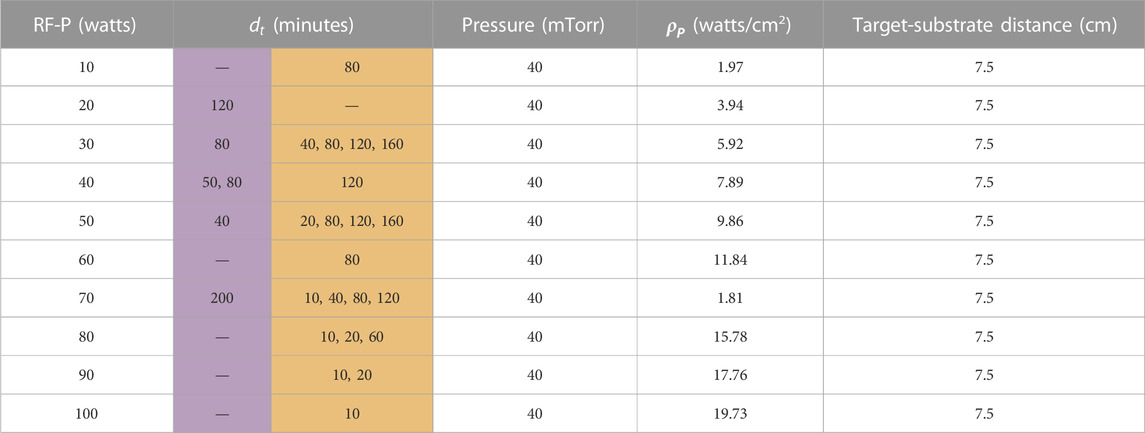
TABLE 1. Deposition parameters used to grow our SiNX thin films. The orange column indicates the
2.2 Sputtering and characterization equipment
Our RF magnetron sputtering equipment was built by the silicon photonics research group of the UNAM Institute of Physics (IFUNAM). As main characteristics, it has a small 4-L spherical deposition chamber that contains a circular cathode coupled to a 1-inch diameter flat magnetron with a NdFeB magnetic arrangement, a shutter, and a non-rotating substrate holder that allows the target distance to be varied. The equipment has a 13.56 MHz SEREN R301 radio frequency power source optimized with the combination of the SEREN AT3 Automatic Matching Network system and the SEREN MC2 Matching Network controller. This combination allows exceptional control of the RF-P, creating stable plasmas as low as 1 W and working pressures of 1 mTorr.
A JEOL JEM-2010F FastTEM transmission electron microscope (TEM) was used to characterize the structure of our films grown on copper grids. We obtained clear, high-resolution images (HRTEM) and electron diffraction patterns by operating the TEM with an accelerating voltage of 200 kV. Meanwhile, the meso- and microstructural characterization was made with our films grown on glass and monocrystalline silicon substrates. On the one hand, the morphology was studied using a JEOL-JSM-7800F ultra-high resolution scanning electron microscope (SEM) with Schottky field emission and operated with an accelerating voltage from 1 to 15 kV. The SEM was also used to cross-sectionally measure the thickness of our films grown on glass substrates and to qualitatively analyze the elemental composition of the films by energy-dispersive X-ray spectroscopy (EDS) using an X-ray detector adapted to the equipment and an accelerating voltage of 10 kV. On the other hand, the topography of our films was analyzed with a JEOL JSPM-4210 atomic force microscope (AFM) in tapping mode and a high-resolution Mikromasch NSC15 silicon tip with a radius of curvature <10 nm.
The optical transmittance/absorbance spectrum of films grown on glass and fused silica substrates was measured with an Agilent Cary UV-Vis-NIR spectrophotometer equipped with a deuterium lamp and a tungsten lamp that emits radiation in the ultraviolet regions (UV) and visible-near infrared (Vis-NIR) respectively. The instrument has a lamp and detector switch that automatically switches in 350 and 800 nm, respectively. All optical absorbance measurements were made with a normal angle of incidence, an optical range of 200–3,000 nm, and a resolution of 1 nm. The thickness and optical refractive index of our films grown on monocrystalline silicon substrates were measured with a Gaertner L117 nullity ellipsometer equipped with a λ = 632.8 nm Helium-Neon laser and a laser incidence angle of 70° with respect to the normal of the film.
Additionally, we deposited a film with RF-P = 70 W and
2.3 Specimens nomenclature
Each SiNX thin film was named sequentially with the RF-P, the type of substrate, and the
3 Results and discussion
3.1 Determination of the optimal chamber pressure
We first needed to establish a constant working pressure to investigate RF-P’s influence on our films’ properties. To determine what constant pressure we would use, we made three preliminary depositions at RF-P = 50 W and
Figure 1 presents the morphologies of the films observed by TEM and HRTEM. The favored formation of crystalline nanometric particles is evidenced at the highest pressure of 40 mTorr, being lower at the two lower pressures. We believe this is because higher pressure enhances plasma densification by generating more Ar ions, increasing the number and possibly the energy of SiNX “nano-chunks” ejected from the target and promoting their orderly interaction in the substrate, thus allowing a better diffusion of the energetic chunks, giving rise to a greater atomic ordering in the film.
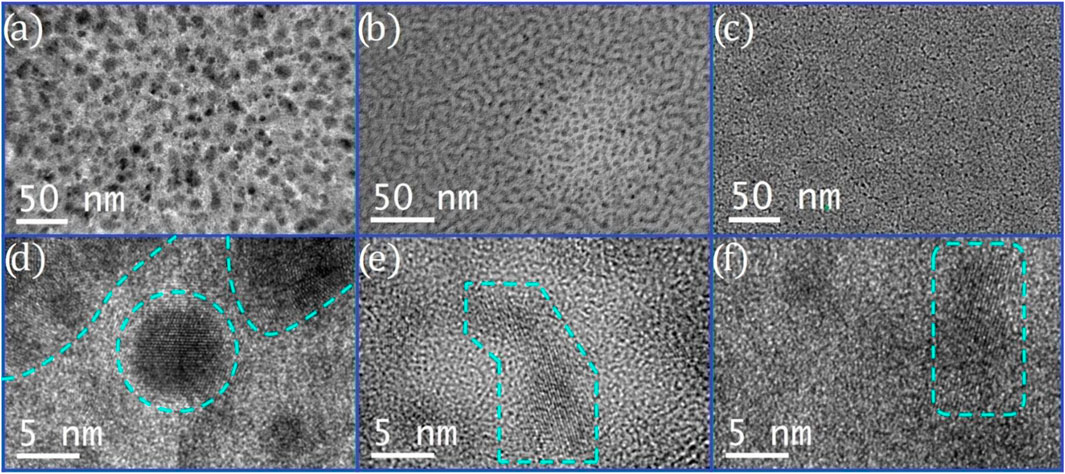
FIGURE 1. Structural morphology characterized by TEM and HRTEM of preliminary films. 50SiN80-40 (A,D), 50SiN80-20 (B,E), and 50SiN80-9 (C,F). Higher magnification micrographs (D–F) demonstrate the presence of crystalline particles in the films, which is quite and easily noticeable in the 50SiN80-40 film.
Figure 1 micrographs were complemented with diffraction patterns obtained exclusively from the 50SiN80-40 film, which show a superposition of rings and points, as shown in Figure 2. These points show the existence of large particles that diffract in the same crystalline plane and have the same crystallographic orientation. On the other hand, the rings denote that the entire film is polycrystalline. Each ring represents a group of particles that diffract in crystal planes belonging to the same family but with different crystallographic orientations. The intense points on the rings indicate that some orientations are preferential. These diffraction patterns were indexed using the crystallographic information reported by Yang et al., determining that the crystalline structure of the particles in the film corresponds to the α phase of silicon nitride (α-Si3N4) [44]. The structural results of these films are both interesting and relevant since it has been widely reported in the literature that SiNX thin films obtained by sputtering techniques at room temperature are amorphous [2, 18, 26, 29, 35], and the possibility that there may be a slight formation of crystalline Si3N4 particles on an amorphous matrix has been overlooked [34].
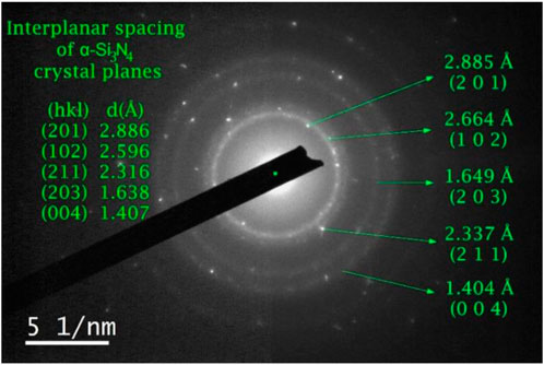
FIGURE 2. Indexed diffraction pattern of 50SiN80-40 film. The distance associated with each ring or point chosen corresponds to the reciprocal of the radius of the ring or the distance between the point and the center of the spot (green point) and represents the interplanar distance in real space of the crystalline planes that diffracted said ring or point. Each calculated distance was compared with the interplanar distances reported for the crystal planes of the α-Si3N4 and β-Si3N4 phases [38], found to be quite approximate to the interplanar distances of some α-Si3N4 planes highlighted to the left of the pattern. Below each calculated distance, we present the crystalline plane of the closest interplanar distance.
Figure 3 presents the optical absorbance of the three preliminary films. The 50SiN80-40 film shows the lowest absorbance, which we attribute to the presence of crystalline particles. Crystalline Si3N4 particles may not contribute to allowed energy states within the band gap of the film, helping to reduce its level of structural disorder and minimize the broadening of its valence (VB) and conduction (CB) band tails caused by a disordered structure and the presence of silicon and nitrogen dangling bonds. A structural disorder and dangling bonds increase the optical absorbance of the film, decrease its bandgap energy (
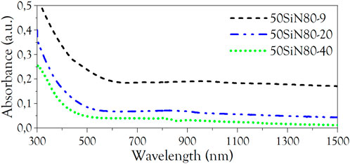
FIGURE 3. Optical absorbance spectra ranging from 300 to 1,500 nm of the three preliminary SiNX thin films.
3.2 Microstructural characterization
Various SiNX thin films were grown on glass substrates, following the deposition parameters indicated in Table 1. We TEM analyzed the structural morphologies of these films. Micrograph Figure 4A reveals the presence of uniformly distributed crystalline particles with diameters less than 15 nm in the 30SiN80 film. A similar pattern is observed in the 30SiN120 film, but with larger particles not exceeding 30 nm in diameter. When deposition time (
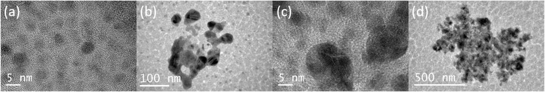
FIGURE 4. Morphological micrographs of the films (A) 30SiN80, (B) 30SiN160, (C) 50SiN80, and (D) 50SiN120. Micrograph (C) shows that the coalescence of smaller particles forms large particles. Hence, when working with a higher
Similar growth was observed in films grown with RF powers of 40 and 50 W. The 50SiN80 film did not present conglomerates but did show very close particles of variable sizes, all less than 40 nm in diameter. Micrograph Figure 4C shows that some of these particles meet at their boundaries and grow together. The 40SiN120 film showed similar behavior; only isolated particles with sizes up to 70 nm in diameter were formed. HRTEM micrographs indicate that these are also made up of smaller particles, similar to what is shown in micrograph Figure 4C. In the 50SiN120 and 50SiN160 films, the evaluation of polycrystalline particles by HRTEM was impossible due to their thicknesses reported in Table 3. Only conglomerates smaller than 1.2 μm were observed, larger in the 50SiN160, as shown in the Figure 4D micrograph. We used the Selected Area Diffraction (SAD) technique in the 50SiN120 and 50SiN160 films. The films showed diffraction patterns of their conglomerates, not individual particles, confirming crystalline particles’ absence or scant presence.
These preliminary results suggest that the formation of clusters is favored in two scenarios: 1) with the same RF-P but increasing the
Both situations can perturb the crystallinity of the particles that make up the final film because the prolonged (case 1) or abundant (case 2) arrival of nobs can cause them to accumulate on each conglomerate or at its boundaries and not have enough energy or time to spread and adopt stable periodic positions, resulting in disorderly growth. The latter justifies why the 30SiN160 and 50SiN120 films stand out for the random presence of conglomerates in a matrix that is observed to be primarily amorphous, unlike the 30SiN120 and 50SiN80 films, and why in the 30SiN120, 40SiN120 and 50SiN120 films, in the order mentioned, a decrease in the presence of uniformly distributed particles is evidenced as the presence of conglomerates and the formation of an amorphous matrix increase.
In the films obtained with RF-P greater than 50 W and
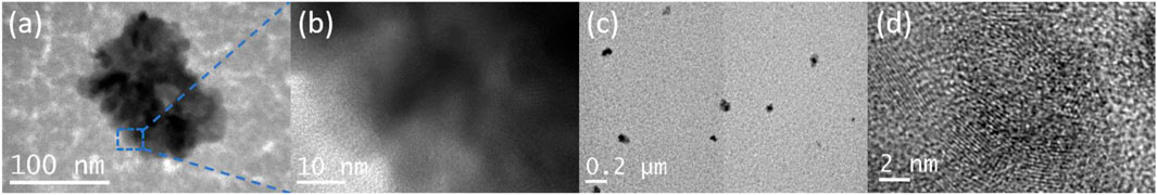
FIGURE 5. Morphological micrographs of the 60SiN80 (A,B), 70SiN80 (C), and 80SiN20 (D) films. Micrograph (B) is an HRTEM image of the in-box section in the 60SiN80 film conglomerate shown in micrograph (A). Micrograph (C) shows the distribution of clusters formed on the 70SiN80 film, and micrograph (D) shows nucleation zones with atomic ordering.
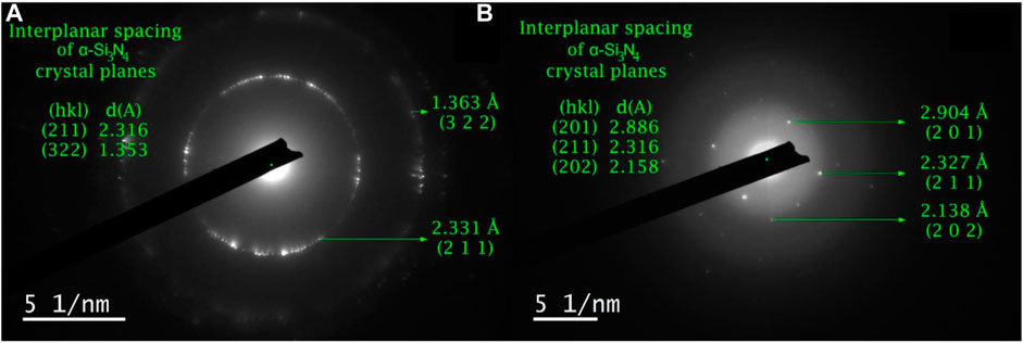
FIGURE 6. Indexed diffraction patterns of the (A) 30SiN80 and (B) 60SiN80 films are used as references to demonstrate the α-Si3N4 crystalline structure of the particles and conglomerates formed in the films of this investigation. The distance associated with each ring or point chosen is the reciprocal of the radius of the ring or the distance between the point and the center of the spot (green point) and represents the interplanar distance of the crystalline planes that diffracted said ring or point. They were pretty close to the interplanar distances of some α-Si3N4 planes highlighted to the left of the pattern [38]. Each calculated distance is associated with a crystalline plane whose interplanar distance is the one it most closely approximates.
Using HRTEM, films grown with RF-P > 50 W exhibited particles with diameters less than 5 nm and distant from clusters, as shown in micrograph Figure 5D. However, those particles were challenging to observe, especially on films grown with RF-P ≥ 80 W. We suspect this is because many ejected SiNX nobs acquire high energy, embedding near their incidence positions or accumulating on the surface without having the possibility of diffusion to acquire stable positions. This phenomenon could inhibit the atomic ordering at the boundaries of already grown particles or the formation of new particles, which is why an amorphous structure prevails in these films.
Finally, a balance between RF-P and
3.3 Chemical and elemental composition analysis
The infrared (IR) optical absorbance spectrum of the 70SiNsm200 film was obtained by FTIR spectroscopy and is shown in Figure 7. Two predominant IR absorption bands are observed; the first, with a maximum peak at 880 cm−1, corresponds to the asymmetric stretching vibration mode of the chemical bonds between silicon and nitrogen (Si-N). The amplitude of this band is related to the film’s amorphicity level, and the number of dangling Si and N bonds generated, especially when a high RF-P is applied [41, 45]. A small shoulder at 965 cm−1 is associated with Si-O bonds which may result from slight oxygen contamination due to environmental exposure or oxygen residue in the deposition chamber, even after high vacuum cleaning [39, 40]. It is known that silicon has high reactivity with oxygen, and surfaces exposed to the environment usually form native oxide layers [16].
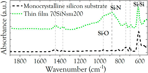
FIGURE 7. Infrared absorbance spectrum of the 70SiNsm200 film, the broad absorption band peaking at 880 cm−1 corresponds to Si-N chemical bonds. The tall and narrow band centered at 610 cm−1 is a contribution from the Si-Si bonds present in the silicon substrate.
On the other hand, the 70SiNsm200 film is not thick enough (530.7 nm) to minimize the contribution of the substrate to the absorbance spectrum obtained with this technique. For this reason, the second narrow absorption band, centered at 610 cm−1, coincides with the IR absorption of the Si-Si bonds of the substrate [16]. The small bands that coincide in the spectra of the substrate and the film are caused by humidity inside the measurement chamber of the equipment. This chemical analysis complements the structural results, as it demonstrates that our films are indeed SiNX by determining the presence of Si-N bonds in the film.
Table 2 summarizes the EDS measurements of the elemental composition of various films. Measurements of a pristine glass substrate and the magnetron anode are included to identify their constituent elements and correlate them with the film measurements. The N readings correspond to the films, and the presence of oxygen was confirmed, one part due to the substrate being glass, and the other as a contaminant, a result of the deposition process and the exposure of the film to the environment.
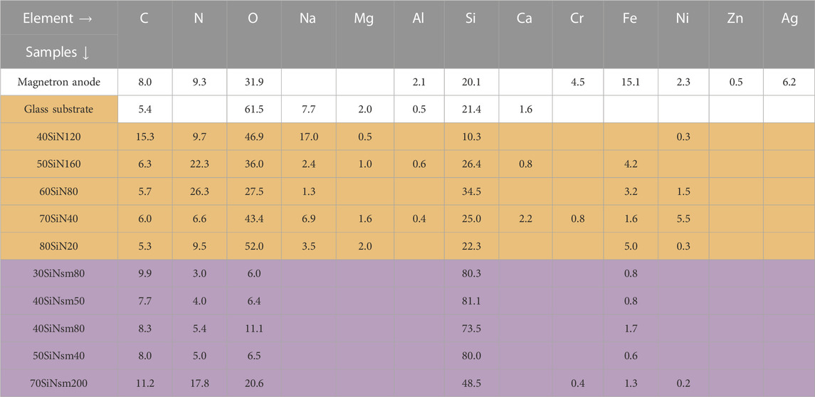
TABLE 2. Atomic percentages of the elements detected by EDS in various SiNX thin films, a glass substrate, and the magnetron anode. The anode has an N reading because it was measured after making the first depositions. N was deposited on its surface by the nearby pulverization of the target. Films grown on glass or monocrystalline silicon with their detected elements are highlighted with ocher or purple color, respectively.
In our measurements, the elements of the glass substrate appear in addition to Si (C, O, Na, Mg, Al, and Ca) because the electron beam passes through the film and excites the atoms on the surface of the substrate due to the low thicknesses of our films (less than 530.7 nm) and the high acceleration voltage applied. A slight contaminating presence of Fe, Cr, or Ni from the anode was detected since it is prone to pulverization, especially when working with high RF-P values. Since the substrates contain Si in their composition, this element is included in the measurement, which makes it impossible to determine the exact percentage of Si present in the film. This situation does not happen with N since this element is absent in the composition of the substrates and the anode of the magnetron.
The presence of silicon in all substrates limits the determination of exact values for the amount of Si and the stoichiometry in our films. However, given the low percentage of N compared to that of Si in almost all the samples and the tendency of various investigations to obtain predominantly Si-rich SiNX thin films, even using a reactive environment with Ar and N2 gases [16, 26, 27, 31, 32], we consider highly probable that our films grown in a non-reactive environment are also silicon-rich.
3.4 Morphological and topographic analysis
The morphology of all the films grown in this study is similar. The SEM observations present a uniform and granular surface formed by nanometer particles that grow together, as illustrated in Figure 8. The growth of the films is governed by the Volmer-Weber model, which is characterized by the formation of islands of material that coalesce at their borders, providing continuity and homogeneity to the film. From the zenithal plane, these islands are seen as particles.
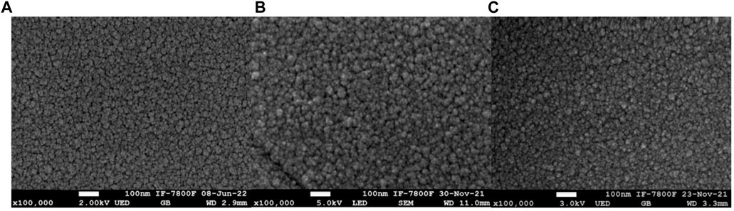
FIGURE 8. Superficial morphology of the films (A) 50SiN80-40, (B) 60SiN80, and (C) 70SiN40. In the lower-left part of the 60SiN80 micrograph, one can see a dark area that we associate with a ditch in the glass substrate reproduced on the film.
Glass is known to have surface defects that influence the growth and properties of a film [41, 42]. We observed these defects’ influence on our films’ growth by means of SEM and AFM techniques. The reproduction of glass surface defects was noted in films deposited with a RF-P of 30 W, even at a high
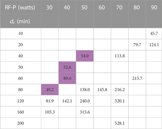
TABLE 3. Average thicknesses of the SiNX thin films measured by cross section in SEM or null ellipsometry (purple boxes). The thickness of the 70SiN200 film was very close to that of the 70SiNsm200 film (530.7 nm).
The morphology of the films formed on monocrystalline silicon substrates also presented granular continuous characteristics and no surface defects, results that were expected considering that they replicate the smooth surface of the substrate. The 30SiNsm80, 40SiNsm50, and 50SiNsm40 films, whose thicknesses are similar, 49.2, 52.6, and 54 nm, respectively, exhibited quite similar morphologies regarding continuity and grain size. Although it is likely that the surface roughnesses of these three films are also similar, it was not possible to characterize their topographies using AFM. We associate this with the possible low surface roughness that they may have due to the replica of the smooth surface of the substrate, which prevents an adequate interaction between the tip of the cantilever and the surface material to detect areas with significant height differences.
The topographies of our films, shown in Figure 9, show the presence of islands of material whose proximity, coalescence, and surface continuity are enhanced by increasing the RF-P. In fact, the growth of the films followed the Volmer-Weber model, as deduced from the morphological analysis. The RMS value of films decreases with increasing
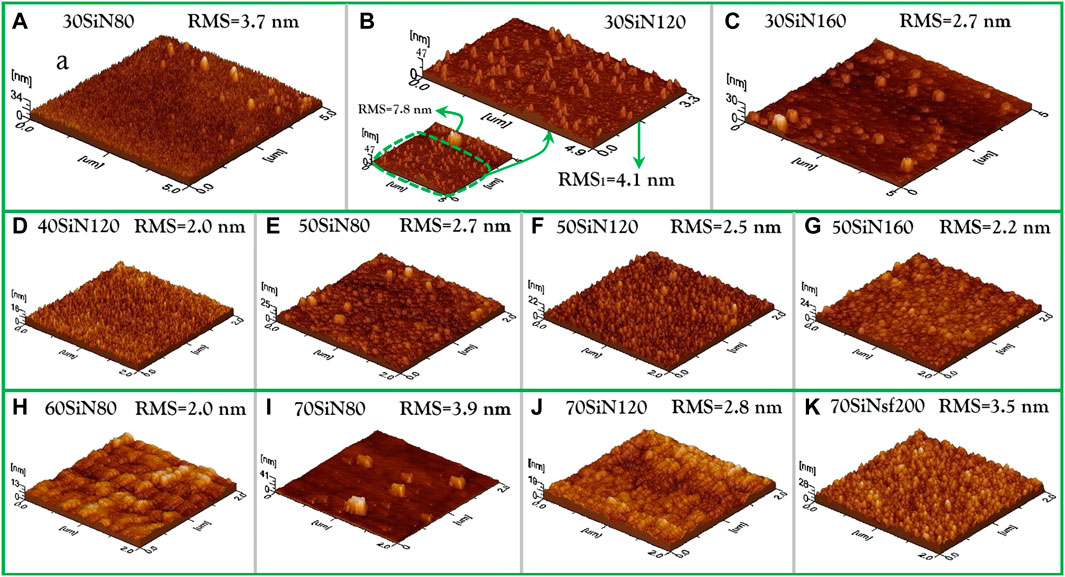
FIGURE 9. Topographic micrographs of several films grown in the investigation. The figure shows analysis areas of 4 and 25 μm2. Each micrograph specifies the film to which it belongs and its RMS roughness (A) 30SiN80, (B) 30SiN120, (C) 30SiN160, (D) 40SiN120, (E) 50SiN80, (F) 50SiN120, (G) 50SiN160, (H) 60SiN80, (I) 70SiN80, (J) 70SiN120, (K) 70SiNsf200. In (B), the rectangular area is magnified to discard the enormous mountain of material from the RSM measurement because it is considered a surface defect of the glass substrate imaged on the film.
The phenomenon of low surface roughness occurs thanks to the constant incidence of nobs with enough energy to diffuse and reach the deep zones generated by the coalescence of the islands’ borders, thus favoring a superficial continuity with low roughness. In contrast, when RF-P = 30 W is used, the reduced energy of the incident nobs promotes low mobility, leading to zonal island growth with poor coalescence and limiting film uniformity and continuity. The high RMS roughness values support the above. Furthermore, the low surface roughness phenomenon is influenced by the reproducibility of glass surface defects in these extremely thin films (<105.3 nm). As seen in micrograph Figure 9B, a large mountain of substrate material generates a considerable variation in the RMS roughness of the analyzed area. Films developed with RF-P ≥ 70 W also show high RMS values (>2.7 nm). We consider that this happens because the incident atoms are highly energetic. At the same time, some diffuse better, favoring the film’s continuity, and others adsorb near their arrival points, favoring an elongated growth of the islands of coalesced material, as seen in the micrograph of Figure 9K.
3.5 Film thickness and deposition rates
The thickness of the films was determined by measuring the cross-section in the Scanning Electron Microscope (SEM) to carry out the optical characterization as shown in Figure 10B. Table 3 shows the average thicknesses of each film.
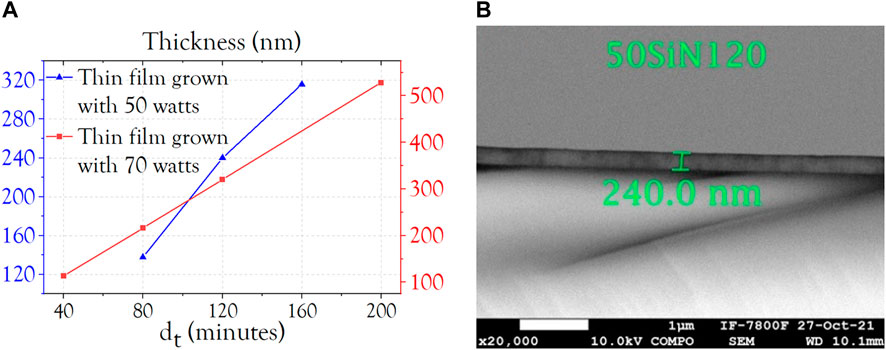
FIGURE 10. (A) Approximately linear relationship of the
It was observed that the deposition rates (
Given this finding, it was reasonable to assume that two films grown with 40 and 50 W could yield a similar result. Therefore, deposition times (
3.6 Optical properties
The optical absorbance of the films, measured by UV-Vis-NIR spectrophotometry, turns out to be low in the Vis-NIR region and is strongly influenced by the radiofrequency powers and the deposition times (
Figure 11A compares the absorbance spectra of films deposited with a
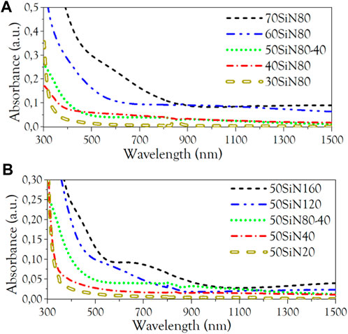
FIGURE 11. Optical absorbance spectra of SiNX thin films grown with (A) different RF-P and
Contaminants such as oxygen and silicon dangling bonds give rise to allowed energy states inside the bandgap of the film, while N dangling bonds broaden the tails of their valence (VB) and conduction bands (BC). The above leads to a shift of the absorption edge towards the NIR, increasing the optical absorbance and decreasing the film’s bandgap energy (
On the other hand, while the optical transmittance (T) is the product of a ratio between the transmitted (
By comparing the absorbance spectra, as shown in Figure 11B, it is evident that the absorbance of the films also increases, and their absorption edge shifts towards the NIR when working with higher
By using the absorbance and thickness of a film, it is possible to calculate the spectrum of its absorption coefficient (
In this regard, Zanatta proposed a simple and efficient method to estimate the
In this study, we use the model proposed by Zanatta. The calculated bandgap energies (
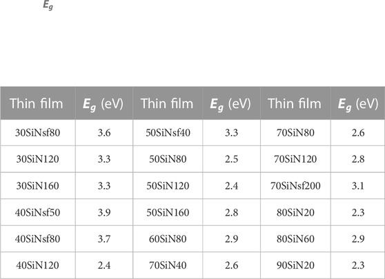
TABLE 4.
A slight downward trend of the
4 Conclusion
In this study, we examined the growth of SiNX thin films by radiofrequency-assisted non-reactive magnetron sputtering at room temperature using an almost stoichiometric Si3N4 target. We determined that it is possible to obtain silicon-rich SiNX films with the formation of particles or polycrystalline conglomerates of α-Si3N4 that increase in size, either maintaining or losing atomic ordering, depending on the combination of RF-P and
We have identified a threshold between RF-P and
On the other hand, the thickness of the films increases with the increase of the RF-P and the
The increase in optical absorbance and the enhancement of the shift of the absorption edge towards the NIR are directly related to the density of dangling Si and N bonds, the stoichiometry, and the structural disorder of the film, and they occur when higher RF-P or
Data availability statement
The original contributions presented in the study are included in the article/Supplementary material, further inquiries can be directed to the corresponding author.
Author contributions
EB-M: Data curation, Formal Analysis, Investigation, Methodology, Writing–original draft. AR-G: Data curation, Formal Analysis, Investigation, Methodology, Writing–original draft, Conceptualization, Funding acquisition, Project administration, Resources, Supervision, Validation, Visualization, Writing–review and editing.
Funding
The author(s) declare financial support was received for the research, authorship, and/or publication of this article. All funding for the realization and publication of this research work came from the projects: a) PAPIIT-UNAM, project number: IN109020, b) PAPIIT-UNAM project number: IN111723, and c) CONACYT—Apoyos para Adquisición y Mantenimiento de Infraestructura en Instituciones y Laboratorios de Investigación Especializada 2019, project number: 299881 which are under the technical administration of Arturo Rodríguez-Gómez.
Acknowledgments
The first author wants to acknowledge the Consejo Nacional de Humanidades, Ciencias y Tecnologías—México for the master’s in science scholarship, CVU No. 1091232. The authors would like to acknowledge the support provided by Roberto Hernández Reyes, Samuel Tehuacanero Cuapa, and Juan Gabriel Morales Morales for technical assistance in TEM, SEM, and sample preparation, respectively.
Conflict of interest
The authors declare that the research was conducted in the absence of any commercial or financial relationships that could be construed as a potential conflict of interest.
Publisher’s note
All claims expressed in this article are solely those of the authors and do not necessarily represent those of their affiliated organizations, or those of the publisher, the editors and the reviewers. Any product that may be evaluated in this article, or claim that may be made by its manufacturer, is not guaranteed or endorsed by the publisher.
References
1. Kaloyeros AE, Jové FA, Goff J, Arkles B. Review—silicon nitride and silicon nitride-rich thin film technologies: Trends in deposition techniques and related applications. ECS J Solid State Sci Technol (2017) 6:P691–P714. doi:10.1149/2.0011710jss
2. Kaloyeros AE, Pan Y, Goff J, Arkles B. Review—silicon nitride and silicon nitride-rich thin film technologies: State-of-the-Art processing technologies, properties, and applications. ECS J Solid State Sci Technol (2020) 9:063006. doi:10.1149/2162-8777/aba447
3. Hegedüs N, Balázsi K, Balázsi C. Silicon nitride and hydrogenated silicon nitride thin films: A review of fabrication methods and applications. Materials (Basel) (2021) 14:5658–21. doi:10.3390/ma14195658
4. Xiong W, Wang G, Li J, Zhao C, Wang W, Radamson HH. SiN-based platform toward monolithic integration in photonics and electronics. J Mater Sci Mater Electron (2021) 32:1–18. doi:10.1007/s10854-020-04909-z
5. Liao C, Wang W, Wang J, Han L, Qiu S, Song L, et al. Magnetron sputtering deposition of silicon nitride on polyimide separator for high-temperature lithium-ion batteries. J Energ Chem (2021) 56:1–10. doi:10.1016/j.jechem.2020.07.046
6. Beck RB, Giedz M, Wojtkiewicz A, Kudła A, Jakubowski A. PECVD formation of ultrathin silicon nitride layers for CMOS technology. Vacuum (2003) 70:323–9. doi:10.1016/S0042-207X(02)00665-6
7. Gleskova H, Wagner S, Gašparík V, Kováč P. Low-temperature silicon nitride for thin-film electronics on polyimide foil substrates. Appl Surf Sci (2001) 175–176:12–6. doi:10.1016/S0169-4332(01)00050-2
8. Sazonov A, Nathan A, Striakhilev D. Materials optimization for thin film transistors fabricated at low temperature on plastic substrate. J Non Cryst Sol (2000) 266:1329–34. doi:10.1016/s0022-3093(99)00946-1
9. Singh J, Johnson J, Singh G, Bhatia A, Barnwal RP, Kaur IP. Fluorescent quantum dots (QDs): A theranostic tool for breast cancer management. Biomed Translational Res (2022) 371–93. doi:10.1007/978-981-16-4345-3_23
10. Rodríguez-Gómez A, Moreno-Rios M, García-García R, Pérez-Martínez AL, Reyes-Gasga J. Role of the substrate on the growth of silicon quantum dots embedded in silicon nitride thin films. Mater Chem Phys (2018) 208:61–7. doi:10.1016/j.matchemphys.2018.01.032
11. Muñoz-Rosas AL, Rodríguez-Gómez A, Arenas-Alatorre JA, Alonso-Huitrón JC. Photoluminescence enhancement from silicon quantum dots located in the vicinity of a monolayer of gold nanoparticles. RSC Adv (2015) 5:92923–31. doi:10.1039/C5RA19114A
12. Rodríguez A, Arenas J, Pérez-Martínez AL, Alonso JC. Role of ammonia in depositing silicon nanoparticles by remote plasma enhanced chemical vapor deposition. Mater Lett (2014) 125:44–7. doi:10.1016/j.matlet.2014.03.144
13. Rodríguez-Gómez A, Escobar-Alarcón L, Serna R, Cabello F, Haro-Poniatowski E, García-Valenzuela A, et al. Modeling of the refractive index and composition of luminescent nanometric chlorinated-silicon nitride films with embedded Si-quantum dots. J Appl Phys (2016) 120:145305. doi:10.1063/1.4964812
14. Wang Y, Qu H, Wang Y, Dong F, Chen Z, Zheng W. Radio frequency plasma-enhanced reactive magnetron sputtering deposition of α-SiNx on photonic crystal—laser diodes for facet passivation. ACS Omega (2019) 4:20205–11. doi:10.1021/acsomega.9b02452
15. Muñoz-Rosas A, Rodríguez-Gómez A, Alonso-Huitrón J. Enhanced electroluminescence from silicon quantum dots embedded in silicon nitride thin films coupled with gold nanoparticles in light emitting devices. Nanomaterials (2018) 8:182. doi:10.3390/nano8040182
16. Signore MA, Sytchkova A, Dimaio D, Cappello A, Rizzo A. Deposition of silicon nitride thin films by RF magnetron sputtering: A material and growth process study. Opt Mater (Amst) (2012) 34:632–8. doi:10.1016/j.optmat.2011.09.012
17. Santana G, Morales-Acevedo A. Optimization of PECVD SiN:H films for silicon solar cells. Sol Energ Mater Sol Cell (2000) 60:135–42. doi:10.1016/S0927-0248(99)00078-1
18. Kulczyk-Malecka J, Kelly PJ, West G, Ridealgh JA. Diffusion studies in magnetron sputter deposited silicon nitride films. Surf Coat Technol (2014) 255:37–42. doi:10.1016/j.surfcoat.2013.11.027
19. Sommer T, Mange N, Wegmann P, Poot M. Efficient adiabatic-coupler-based silicon nitride waveguide crossings for photonic quantum computing. Opt Lett (2023) 48:2981. doi:10.1364/OL.491869
20. Richter LJ, Ihlemann J. Photoluminescence enhancement of silicon nanocrystals by excimer laser implanted gold nanoparticles. Appl Phys A (2022) 128:764. doi:10.1007/s00339-022-05906-1
21. Porcel MAG, Hinojosa A, Jans H, Stassen A, Goyvaerts J, Geuzebroek D, et al. [INVITED] Silicon nitride photonic integration for visible light applications. Opt Laser Technol (2019) 112:299–306. doi:10.1016/j.optlastec.2018.10.059
22. Wilmart Q, El Dirani H, Tyler N, Fowler D, Malhouitre S, Garcia S, et al. A versatile silicon-silicon nitride photonics platform for enhanced functionalities and applications. Appl Sci (2019) 9:255. doi:10.3390/app9020255
23. Ding B, Yu X, Lu H, Xiu X, Zhang C, Yang C, et al. Third-order optical nonlinearity in silicon nitride films prepared using magnetron sputtering and application for optical bistability. J Appl Phys (2019) 125. doi:10.1063/1.5085234
24. Frigg A, Boes A, Ren G, Abdo I, Choi D-Y, Gees S, et al. Low loss CMOS-compatible silicon nitride photonics utilizing reactive sputtered thin films. Opt Express (2019) 27:37795. doi:10.1364/oe.380758
25. Dutt A, Salinas RA, Martínez-Tolibia SE, Ramos-Serrano JR, Jain M, Hamui L, et al. Silicon compound nanomaterials: Exploring emission mechanisms and photobiological applications. Adv Photon Res (2023) 4:2300054. doi:10.1002/adpr.202300054
26. Dergez D, Schneider M, Bittner A, Pawlak N, Schmid U. Mechanical and electrical properties of RF magnetron sputter deposited amorphous silicon-rich silicon nitride thin films. Thin Solid Films (2016) 606:7–12. doi:10.1016/j.tsf.2016.03.029
27. Vila M, Prieto C, Ramírez R. Electrical behavior of silicon nitride sputtered thin films. Thin Solid Films (2004) 459:195–9. doi:10.1016/j.tsf.2003.12.082
28. Rodríguez-López R, Soto-Valle G, Sanginés R, Abundiz-Cisneros N, Águila-Muñoz J, Cruz J, et al. Study of deposition parameters of reactive-sputtered Si3N4 thin films by optical emission spectroscopy. Thin Solid Films (2022) 754:139313. doi:10.1016/j.tsf.2022.139313
29. Mustafa MK, Majeed U, Iqbal Y. Effect on silicon nitride thin films properties at various powers of RF magnetron sputtering. Int J Eng Technol (2018) 7:39. doi:10.14419/ijet.v7i4.30.22000
30. Baptista A, Silva F, Porteiro J, Míguez J, Pinto G. Sputtering physical vapour deposition (pvd) coatings: A critical review on process improvement and market trend demands. Coatings (2018) 8:402. doi:10.3390/COATINGS8110402
31. Takeyama MB, Sato M, Nakata Y, Kobayashi Y, Nakamura T, Noya A. Characterization of silicon nitride thin films deposited by reactive sputtering and plasma-enhanced CVD at Low temperatures. Jpn J Appl Phys (2014) 53:05GE01–5. doi:10.7567/JJAP.53.05GE01
32. da Silva Zambom L, Domingues Mansano R, Paula Mousinho A. Low-temperature deposition of silicon oxide and silicon nitride by reactive magnetron sputtering. Microelectronics J (2009) 40:66–9. doi:10.1016/j.mejo.2008.07.017
33. Gudmundsson JT. Physics and technology of magnetron sputtering discharges. Plasma Sourc Sci Technol (2020) 29:113001. doi:10.1088/1361-6595/abb7bd
34. De Luca D, Di Gennaro E, De Maio D, D’Alessandro C, Caldarelli A, Musto M, et al. Tuning silicon nitride refractive index through radio-frequency sputtering power. Thin Solid Films (2021) 737:138951. doi:10.1016/j.tsf.2021.138951
35. Liang HY, Zhao QN, Gao F, Yuan WH, Dong YH. Effect of RF sputtering power on the structural, optical and hydrophobic properties of SiN<sub>x</sub> thin film. Adv Mater Res (2011) 194–196:2340–6. doi:10.4028/www.scientific.net/AMR.194-196.2340
36. Cisneros-Contreras IR, López-Ganem G, Sánchez-Dena O, Wong YH, Pérez-Martínez AL, Rodríguez-Gómez A. Al-doped ZnO thin films with 80% average transmittance and 32 Ohms per square sheet resistance: A genuine alternative to commercial high-performance indium tin oxide. Physics (College Park Md) (2023) 5:45–58. doi:10.3390/physics5010004
37. León-Guillén R, Muñoz-Rosas AL, Arenas-Alatorre JA, Alonso-Huitrón JC, Pérez-Martínez AL, Rodríguez-Gómez A. Experimental study of the influence of CH 4 and H 2 on the conformation, chemical composition, and luminescence of silicon quantum dots inlaid in silicon carbide thin films grown by remote plasma-enhanced chemical vapor deposition. ACS Omega (2022) 7:19640–7. doi:10.1021/acsomega.2c01384
38. Yang P, Fun H-K, Rahman IA, Saleh MI. Two phase refinements of the structures of α-Si3N4 and β-Si3N4 made from rice husk by Rietveld analysis. Ceram Int (1995) 21:137–42. doi:10.1016/0272-8842(95)95885-L
39. Sanginés R, Abundiz-Cisneros N, Hernández Utrera O, Diliegros-Godines C, Machorro-Mejía R. Plasma emission spectroscopy and its relation to the refractive index of silicon nitride thin films deposited by reactive magnetron sputtering. J Phys D Appl Phys (2018) 51:095203. doi:10.1088/1361-6463/aaa8d4
40. Kim JH, Chung KW. Microstructure and properties of silicon nitride thin films deposited by reactive bias magnetron sputtering. J Appl Phys (1998) 83:5831–9. doi:10.1063/1.367440
41. Gupta PK, Inniss D, Kurkjian CR, Zhong Q. Nanoscale roughness of oxide glass surfaces. J Non Cryst Sol (2000) 262:200–6. doi:10.1016/S0022-3093(99)00662-6
42. Khachatryan H, Lee S-N, Kim K-B, Kim H-K, Kim M. Al thin film: The effect of substrate type on Al film formation and morphology. J Phys Chem Sol (2018) 122:109–17. doi:10.1016/j.jpcs.2018.06.018
43. Zanatta AR, Chambouleyron I. Absorption edge, band tails, and disorder of amorphous semiconductors. Phys Rev B (1996) 53:3833–6. doi:10.1103/PhysRevB.53.3833
44. Attaf A, Benkhedir ML, Aida MS. Influence of substrate bombardment on sputtered a-Si:N thin film properties. Phys B Condens Matter (2005) 355:270–9. doi:10.1016/j.physb.2004.11.004
Keywords: silicon nitride thin films, silicon quantum dots, RF-sputtering, HRTEM, α-Si3N4
Citation: Barrera-Mendivelso ES and Rodríguez-Gómez A (2023) Thin films of silicon nitride deposited at room temperature by non-reactive magnetron sputtering: radiofrequency power and deposition time influence on the formation of α-Si3N4 and its optical properties. Front. Phys. 11:1260579. doi: 10.3389/fphy.2023.1260579
Received: 18 July 2023; Accepted: 09 August 2023;
Published: 22 August 2023.
Edited by:
Stefanos Papanikolaou, National Centre for Nuclear Research, PolandReviewed by:
Francisco Javier Dominguez Gutierrez, National Center for Nuclear Research, PolandJianbao Zhao, Canadian Light Source, Canada
Copyright © 2023 Barrera-Mendivelso and Rodríguez-Gómez. This is an open-access article distributed under the terms of the Creative Commons Attribution License (CC BY). The use, distribution or reproduction in other forums is permitted, provided the original author(s) and the copyright owner(s) are credited and that the original publication in this journal is cited, in accordance with accepted academic practice. No use, distribution or reproduction is permitted which does not comply with these terms.
*Correspondence: Arturo Rodríguez-Gómez, YXJvZHJpZ3VlekBmaXNpY2EudW5hbS5teA==