 Jianwei Wang1
 Zhenjun Fan
 Haifeng Liu
- 1School of Science, China University of Geosciences, Beijing, China
- 2State Key Laboratory of Integrated Optoelectronics, Institute of Semiconductors, Chinese Academy of Sciences, Beijing, China
- 3Beijing Huairou Instruments and Sensors Co., Ltd., Beijing, China
We realize a tunable narrowband and broadband coexisting absorber based on a simple step-shaped all-metal grating structure. The absorber presents an ultra-narrow absorption band of 1.5 nm and a relatively broad absorption band of 29.8 nm, both with nearly 100% absorption in the infrared region. The mechanism underlying the dual-band perfect absorption is the interaction between two diffraction coupled surface plasmon polariton (SPP) modes with one of them modulated by a cavity resonance. Influences of structure parameters on the absorption performance are numerically investigated. It is found that the positions of the two perfect absorption peaks can be easily tuned both independently and together by changing the structural parameters. In addition, the designed grating structure presents excellent sensing performance with sensitivity and figure of merit as high as 2,514 nm/RIU and 1,600 RIU−1, respectively. The excellent sensing performance, flexible tenability and simple structure design endow this grating absorber with great potential in high-precision biochemical sensing applications.
1 Introduction
Perfect plasmonic absorbers have been rapidly developed due to their applications such as energy harvesting [1–3], thermal emitting [4,5], structural color [6], stealth devices [7,8] and biochemical sensing [9–11]. A basic method to obtain perfect absorptions is to bring about electromagnetic resonances, for example, metallic structures patterned at subwavelength scales give rise to various resonances and the absorption band linewidths enabled by which are generally tens to hundreds of nanometers. In practical applications, some special absorption bandwidths, such as ultra-broad band with several microns and ultra-narrow band with several nanometers even sub-nanometer are also of great desire. For example, broadband uniform absorption in the visible to infrared spectral range has wide applications in thermophotovoltaics and solar harvesting. In contrast, in fields of optical sensing, modulation, and thermal emission tailoring, it is desired to realize absorption within an extremely narrow spectral range. Plasmonic resonant absorption based on different physical mechanisms is the foundation for achieving broad and narrow band absorbers. Boadband absorbers usually rely on combinations of multiple closely located resonant absorption bands [12,13] while narrowband absorbers depend on the coupling and hybridization among different resonant modes, for example, Fano resonance [14,15], electromagnetically induced transparency (EIT) [16,17], bound states in the continuum (BIC) [18,19], surface lattice resonances (SLR) [20,21] and so on.
In recent years, with the demand for high sensitivity sensing in biochemistry, extremely narrow band absorbers are of great importance and have attracted increasing attention. To date, various platforms have been proposed to realize high-performance narrowband absorption. For example, utilizing high quality factor characteristics of a BIC resonance, by introducing a graphene layer into an all-dielectric compound grating, a quasi-BIC resonance was excited and a perfect absorption peak with full width at half maximum (FWHM) as narrow as 5.7 nm was obtained [22]. By exciting a quadrupolar plasmonic lattice resonance in a horizontal metal–insulator–metal (MIM) grating, a bandwidth of 1.2 nm resonant absorption peak was obtained [23]. By optimizing structural parameters of a thin sliver grating, an ultra-narrow band absorber with linewidths as narrow as 0.4 nm was obtained [24]. By making use of surface plasmonic mode with a small dissipation rate propagating in an asymmetric metagrating structure, a perfect optical absorption with a bandwidth of 0.28 nm was obtained [25]. Despite extensive researches have been conducted to reduce the absorption band linewidth and some of them have been successfully reduced to sub-nanometer scale, most of the works focused on a single resonant peak. Nowadays, with the widespread use of artificial intelligence and machine learning, improving the accuracy of a single detection signal is far from enough. Increasing the number of the detection signals and improving their diversity and flexibility have become an effective route to further improve the detection sensitivity. Some multiple absorption peaks with narrow bands have also been reported and they are usually obtained through exciting of and coupling between several different resonant mechanisms in complex structures. For example, when SPP, localized surface plasmon resonance (LSPR), Fabry-Perot (F-P) resonance and Wood’s anomalies are simultaneously excited in a double-layer metal grating, three absorption peaks were obtained through the interactions between the resonances [26]. By introducing a nano-slit arrays into a photonic film, combination effect of nano-slit cavity resonances and photonic waveguide resonances can be realized and four different ultra-narrow band absorption peaks were obtained [27]. By simultaneous excitation SPP mode and Wood’s anomalies in a square-patch-based MIM structure, a dual narrow-band absorber was obtained [28]. However, through detailed investigation, it is found that the absorption peaks in these absorbers are often interrelated, and their positions cannot be adjusted independently. In addition, these structures are usually complex multilayer structures composed of both dielectrics and metals, which makes them not convenient enough in manufacturing and applications. More importantly, when these absorbers are used as refractive index (RI) sensors, the fields localized in the dielectric layers will limit the overlap of the field distribution with analyte and further decrease their detection sensitivity.
In this paper, we design and propose a simple step-shaped all-metal grating as shown in Figure 1A, which can achieve perfect absorption peaks including both an ultra-narrow bandwidth as narrow as 1.5 nm and a broad bandwidth of tens of nanometers in the near infrared region. Besides, these two perfect absorption peaks can be easily tuned either individually or together via varying the geometric parameters. This feature makes it possible to better meet the measurement requirements of versatile complex scenarios. More importantly, the absorber is an all-metal structure, therefore its resonant field can be fully distributed in the analyte. Together with the ultra-narrow absorption band enabled by the elaborately designed resonant mechanism, this grating absorber exhibits excellent RI sensing performance. While remaining nearly 100% absorption, the sensing sensitivities of its two absorption peaks can still reach over 2,000 in both air and solution environments. To our knowledge, this is currently an excellent sensitivity value for RI sensors.
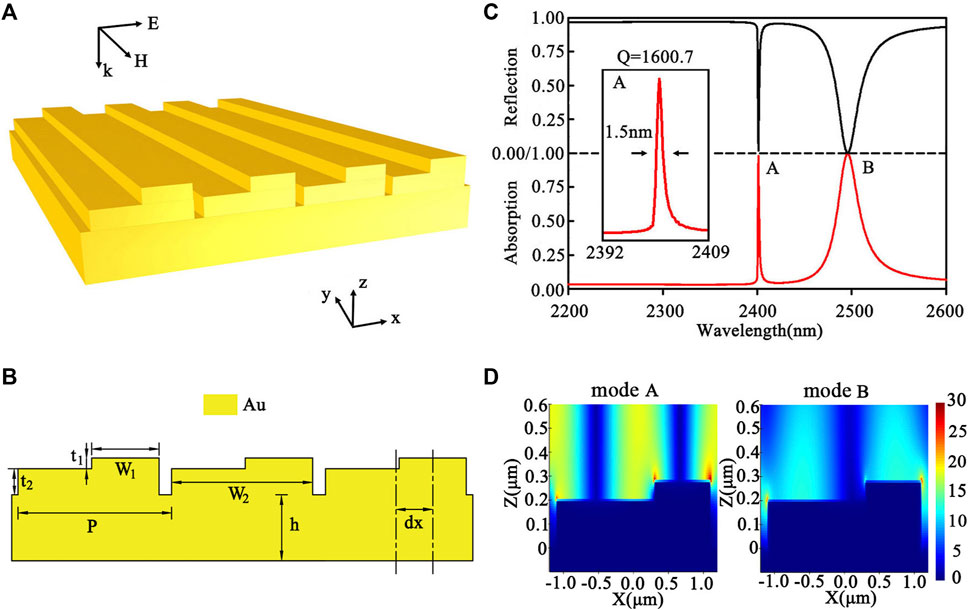
FIGURE 1. (A) Schematic of the proposed Au step-shaped grating structure. (B) Cross-sectional view of the proposed grating structure. (C) Reflection and absorption spectra of the Au step-shaped grating structure with P = 2,400 nm, w1 = 800 nm, t1 = 80 nm, w2 = 2,200 nm, t2 = 200 nm, dx = 700 nm and h = 500 nm. (D) Electric intensity distributions within one grating period at the resonant wavelengths of mode A and mode B.
2 Structure design, absorption properties and mechanism analysis
2.1 Structure and results
The schematic geometry of the proposed step-shaped all-metal grating structure is shown in Figure 1A. For clarity, a coordinate system is also established, in which the grating surface is arranged in the x-y plane. It is a one-dimensional grating and each unit cell of the grating consists of two Au strips with different sizes stacked together. The lower one is wider and the upper one is narrower. In order to demonstrate their geometries more clearly, a cross-sectional view of this structure is also given in Figure 1B. The period of the grating is indicated by P. The widths and thicknesses of the two strips are represented by w1, t1, w2 and t2, respectively. These two strips also have offset in horizontal direction and the lateral shift between them (center to center distance in the x direction) is described by dx. The whole grating is supported by a thick Au substrate with thickness of h. A commercial software (Lumerical, FDTD Solutions) is employed to simulate the interaction between incident wave and the step-shaped grating structure. A linearly polarized light with an electric component in the x-direction (TM polarized) is normally incident to the structure along the backward direction of the z-axis. In the simulation, one period of the grating is chosen to stand for the whole structure, then periodic boundary conditions are used in the x-direction and y-direction, and perfectly matched layer conditions are used in the z-direction. The permittivity of Au is chosen from the material bank of FDTD Solutions as Au (gold)-Palik, which was obtained from Palik’s handbook [29]. As the Au substrate is thick enough, the incident wave will be effectively blocked and absorption is only determined by its reflection, i.e., A (absorption) = 1–R (reflection).
Figure 1C gives the calculated reflection and absorption spectra of the above step-shaped grating. In calculation, the geometric parameters are set as follows: P = 2,400 nm, w1 = 800 nm, t1 = 80 nm, w2 = 2,200 nm, t2 = 200 nm, dx = 700 nm, h = 500 nm. As illustrated by the red solid line in Figure 1C, there are two remarkable perfect absorption peaks (marked as peaks A, and B, respectively) exhibited in the absorption spectrum, which is equivalent to two resonant reflection dips due to the opaque Au film at the bottom of the structure. One can see that these two resonant peaks show obviously different linewidths and spectral positions. The narrower absorption peak A exhibits an obvious asymmetric Fano-type which indicates that it may be generated by coupling of different resonances. It appears at the position of λ = 2,401 nm (near the value of the gating period P), and its FWHM is only about 1.5 nm, resulting in a high quality factor of up to 1600.7. The enlarged illustration of the absorption peak A shows its ultra-narrow resonant linewidth more clearly. In contrast, the absorption peak B in the long-wavelength range possesses a relatively broad linewidth of 29.8 nm. Although this linewidth is dozens of times wider than that of peak A, it is still narrower than those of most plasmonic resonances. Moreover, both the linewidths and the spectral positions of the two peaks can be further optimized and adjusted if needed which will be demonstrated later.
Figure 1D gives the electric intensity distributions within one grating period at the resonant wavelengths of peak A and peak B. It is seen that the electric intensity of mode A is slightly stronger than that of mode B. As for the spatial distribution, the electric field of mode A is mainly distributed above the metal grating, while that of mode B is not only distributed above the metal grating, a small part of it is also distributed in the grating air grooves. These differences imply that the resonance mechanisms of the two resonant modes may be different. The specific reason why the field distribution has such different distribution properties and the absorption characteristics brought by these field distributions will be discussed in detail in the next section.
2.2 Mechanism discussions
It is known that metagratings can support various resonant mechanisms. For example, even in a single-layer grating, there can be up to five or even more resonant mechanisms: SPPs excited on the top and bottom boundaries of the gratings [30,31], LSPR supported by each individual grating strip, cavity mode resonance occurring in the grating slits or grooves [30,31], Rayleigh anomalies that occur when one of the diffraction orders grazes the grating surface [32], phase resonance caused by the destructive interference between radiative light from different slits or grooves [33,34]. Furthermore, coupling and hybridization between these resonant modes will also generate various novel resonances [20,21]. To reveal the cause of the dual resonant absorption peaks given above, we first investigate a simple grating consists of single-layer of periodic Au strips. Figure 2A gives its spectral evolution of the reflection spectra with changing of the strip width, w. In calculation, the period of the single-layer grating still takes value of P = 2,400 nm and the thickness of the Au strip is set to be 80 nm, sitting on an Au substrate with thickness of h = 500 nm. From Figure 2A, it can be seen that there is always a resonant reflection dip appearing around the position λ = P = 2,400 nm. As the width of the Au strip increases, the reflection dip first moves right and then returns back to the position λ = P = 2,400 nm, but always locating at the right side of λ = 2,400 nm. Besides, the linewidth also varies gradually with the positions of the reflection dips. As the resonant wavelength approaches the period of the grating, its linewidth becomes narrower and narrower. While when it deviates from the period of the grating, its linewidth becomes slightly broader. Within the entire evolution process, the linewidth can reach a maximum of 11 nm at w = 1,600 nm and a minimum of 0.9 nm at w = 600 nm. It can be seen that if only a single narrow band perfect absorption is desired, this single layer grating structure already meets the requirements. Its minimum bandwidth is only 0.9 nm which corresponds to a Q-factor as high as 2,700. These results are superior to most reported work using complex structures in the literature.
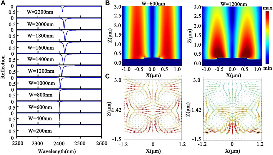
FIGURE 2. (A) Spectral evolution of the reflection spectrum of a single-layer thin Au grating with the width of the Au strips, where the period of the grating is P = 2,400 nm, thickness of the strips is t = 80 nm and thickness of the substrate is h = 500 nm. (B) Distributions of the electric field intensity at resonant wavelengths for w = 600 nm and 1,200 nm. (C) Distributions of the Poynting vector at resonant wavelengths for w = 600 and 1,200 nm.
In order to reveal the underlying physics of the reflection dips, the electric field intensity distributions at the resonant wavelengths are extracted. All the distributions for different strip widths have similar field distribution properties. Figure 2B gives the distributions for widths of 600 and 1,200 nm. One can see that most electric field is located above the grating surface, rather than appearing as a dipole resonance confined near the xy plane where the metal grating strips are located. It means that these resonant dips are not caused by SLR. In addition, if we further expand the field distribution area upwards, we find that the electric field distribution is a typical field distribution of SPP propagating on metal surfaces. It is worth noting that the field distribution of this SPP decays particularly slowly in the direction perpendicular to the grating surface, allowing its penetration depth in air to reach several micros. Besides, when we extract the Poynting vector near the grating surface, as shown in Figure 2C, it is found that at the resonant wavelengths there is no energy flow propagating along the grating surface. In contrast, the incident wave energy circulates within each individual period. This distribution characteristic of the energy flow is similar to that of a standing wave. It indicates that the field distribution is an SPP standing wave formed by the superposition of SPP waves propagating in two opposite directions along the grating surface.
It is known that to excite SPPs, the wave vector matching condition must be satisfied. For the thin grating above, its thin strips or shallow grooves formed between the strips can be regarded as small perturbations to the flat interface. Therefore, kspp formed along the grating surface is approximately equal to that formed at a flat interface between Au film and free space, i.e.,
As for the reason of the perfect absorption and small linewidth of the reflection dips, Rayleigh anomaly also plays an important role. When light is incident normally, within the wavelength range we calculated, when the ±1st diffraction orders propagate grazing the grating surface, Rayleigh anomaly of the grating will occur near the position of
Now the physical mechanism of the above reflection dips of a thin strip grating is clear. For convenience, we refer to it as a diffraction coupled SPP mode. Its absorption value, resonant wavelength, and absorption linewidth can be further tuned by another resonant mechanism. Here we design a cavity mode resonance to implement the modulation role. We select a broad grating strip width, if the width is wide enough, a narrow air groove will be formed between the adjacent strips and a cavity mode resonance will occur in it. The deeper the cavity, the longer the resonance wavelength. Figure 3A gives the spectral evolution of the reflection spectra changing with the strip thicknesses, where the grating period is still P = 2,400 nm and width of the strips is set to be w = 2,200 nm. It can be seen that under the modulation of the cavity mode, the value of the original reflection dip which does not reach 0, can be further reduced to 0. It means that changing the groove depth is able to enhance the absorption. Moreover, as the thickness of the grating strip increases, the depth of the cavity becomes deeper and deeper, as a result, the position of the resonant wavelength continuously redshifts. Because the linewidth of the cavity mode is much larger than that of the diffraction coupled SPP mode, the linewidth of their hybrid modes is also modulated and gradually increases with the increase of the strip thickness. Figure 3B shows the distribution of electric field intensity where the strip thicknesses are 140 and 200 nm, respectively. It is seen that the diffraction coupled SPPs are still excited. However, due to the deviations of the resonant wavelengths from the position of λ = p, the wave vector component in the z-direction increases accordingly and the field distribution becomes more localized towards the grating surface. The magnified field distributions on their right sides are the electric field intensity distributions in the grating grooves when resonance occurs. Obviously, the cavity mode resonance that was not excited for a thin strip grating becomes more and more apparent. It plays a modulation role in the diffraction coupled SPP mode, making the resonant peak redshift and the resonant linewidth increase gradually.
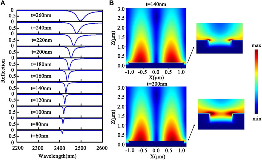
FIGURE 3. (A) Spectral evolution of the reflection spectra of a single-layer Au grating with the thickness of the Au strips, where the period of the grating is P = 2,400 nm, width of the strip is w = 2,200 nm and thickness of the substrate is d = 500 nm. (B) Distributions of the electric field intensity at resonant wavelengths for t = 140 and 200 nm and the magnified fields are their electric field distributions in the grating grooves.
In design of high-performance sensors, coupling and hybridization among different plasmonic modes is an effective strategy to generate new plasmonic resonances and adjust their linewidths and amplitudes. Here, we consider the interaction between two diffraction coupled SPP modes with one of them is designed to be modulated by a cavity mode. As shown in Figure 1A, we stacked two grating strips with different structure sizes (w1 = 800 nm, t1 = 80 nm, w2 = 2,200 nm, t2 = 200 nm) on an Au film, the lateral distance between them is dx. This structure enables it possible to arouse interaction between the two diffraction coupled SPP modes based on the vertical coupling between the two layers of gratings. Figure 4 shows the reflection spectra of the step-shaped grating for different dx. For comparison, the reflection spectra of the gratings consisting of only lower strips (w2 = 2,200 nm, t2 = 200 nm) and only upper strips (w1 = 800 nm, t1 = 80 nm) are also given in the lowest row. As can be seen, when there is no lateral shift between the two strips (dx = 0 nm), the whole structure can be regarded as a simple grating consisting of complex units. The original two split resonances of each grating layer, couple into a total one with a widened linewidth and a compromised deviation away from the position of λ = 2,400 nm. Due to the complex grating units, the scatter effect of the grating becomes more prominent. Besides, due to the enlarged mismatch of the resonant wavelengths between the Rayleigh anomaly and the SPP resonance, the effect of Rayleigh anomaly will also be weakened. As a result, the scattering of the incident light will become even stronger and the absorption cannot reach 100% any longer. At the same time, due to the enhanced scattering loss the linewidth of the resonant dip is accordingly widened. When the two grating strips gradually shift away from each other, the resonance characteristics of the individual single-layer grating start to appear. There are two separate resonance peaks appearing near their original resonant positions. However, the coupling of the two layers of gratings will bring about influences on their respective resonance. For example, as dx gradually increases, when the upper Au strip approaches the right edge of the lower one, the upper strip will also display the confine effect on the light waves, which is equivalent to enhancing the effective depth of the air groove formed between the adjacent lower strips. Therefore, under the influence of the cavity mode resonance, the second resonant wavelength becomes larger and larger. When dx is larger than 400 nm, both of the two resonances achieve nearly 100% absorption, and the space between them can be continuously adjusted, indicating that this step-shaped grating structure has potential to design tunable dual-band absorption sensors.
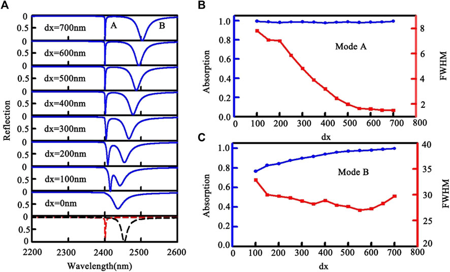
FIGURE 4. (A) Reflection spectral evolution of the step-shaped grating with changing lateral shift dx, where P = 2,400 nm, w1 = 800 nm, t1 = 80 nm, w2 = 2,200 nm and t2 = 200 nm. (B,C) are the absorption value and resonant linewidth varying with the lateral shift dx for mode A and mode B, respectively.
In order to make clear the detailed influences of the coupling effect on their respective resonance properties, Figures 4B, C give the absorption values and linewidths of the two resonant modes varying with the lateral shift dx, respectively. One can see that though the absorption and the resonant linewidth of the two absorption peaks exhibit different evolution trends, when dx increases, especially when the upper and lower strips are close to be aligned at their right ends, both resonant modes exhibit absorption values close to 100%. As for their linewidths, when dx increase, mode B does not display significant variation, however, the linewidth of the mode A decreases significantly. When dx increases to 700, the linewidth can be reduced to 1.5 nm and the corresponding Q-factor reaches 1,600.
For a biosensor, higher absorption and narrower linewidth of the resonance spectrum are essential. In the analysis above, we randomly selected two grating strip widths, 800 and 2,200 nm to investigate the absorption properties. In fact, the absorption and the resonant linewidths of the resonant peaks can be further optimized via adjusting other structural parameters. Here, in order to form an effective cavity with adjacent Au strips at the lower layer, the width of lower strip should be relatively long and the variation range of this width is limited. Therefore, w2 still takes a value of 2,200 nm. We choose w1 as an example to optimize the absorption and resonance performance. Figures 5A, B give the absorption and the linewidths changing with w1 for mode A and B, respectively. In calculation, dx also varies with w1 to maintain the alignment of the upper and lower strips at their right ends. It is seen that both the absorption and FWHM can be optimized individually. For mode A, when w1 is around 700 nm, its FWHM can be optimized to sub-nanometer scale, which is equivalent to obtaining a Q-factor of over 2000, at the same time, its absorption value is still larger than 90%. Moreover, when the absorption of the two modes both approaches 100%, there is still a wide overlap range of the w1 value. If high absorption and narrow linewidth for two resonant modes are both desired, the value of w1 should be selected between 700 and 800 nm.
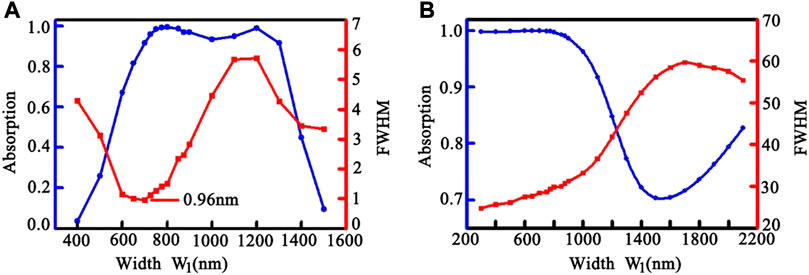
FIGURE 5. (A,B) are the absorption value and resonant linewidth varying with the parameter w1 for mode A and mode B, where P = 2,400 nm, w2 = 2,200 nm, d = 500 nm.
2.3 Tuning performance of the two resonant modes
In practical sensing applications, tuning flexibility between multiple operating wavelengths is crucial as it not only improves detection accuracy but also makes measurement more convenient. In our structure, the two reflection dips (mode A and mode B) of the proposed step-shaped grating structure can be tuned flexibly via changing different parameters. The positions of the two absorption peaks can be adjusted both separately and together. For example, the dependence of reflection spectra on structural period P is demonstrated in Figure 6A, where the other parameters remain unchanged from those used in Figure 1 except that w2 also changes with the period to maintain the air grooves formed between them is always 200 nm wide. One can see that the two resonant reflection dips both have obvious redshifts with the increase of P. The speeds of the redshifts of the two modes are similar, and the spectral spacing between them is almost unchanged. Besides, in the entire evolution process, the reflection of the two modes both remains nearly zero except that the resonance linewidths slightly decrease. This spectral evolution can be easily explained using the characteristics of the diffraction coupled SPPs supported by a thin grating.
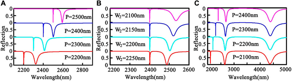
FIGURE 6. Tuning performance of the two reflection dips. (A) Influence of grating period P on the two resonant reflection dips of a thin grating with w1 = 800 nm, w2 = P-200 nm, t1 = 80 nm, t2 = 200 nm. (B) Influence of the lower grating strip width w2 on the reflection spectra with P = 2,400 nm, w1 = 800 nm, t1 = 80 nm, t2 = 200 nm. (C) Influence of grating period P on the two resonant reflection dips of a thick grating with w1 = 800 nm, w2 = 2,200 nm, t1 = 80 nm, t2 = 2,700 nm.
One significant advantage of our proposed absorber is that the two resonant modes can be tuned not only simultaneously, but also individually. There are several parameters that can be employed to adjust the position of the second resonant peak (mode B). According to the former analysis, increasing the value of t2 can directly deepen the grating grooves, thereby causing the mode B to redshift. Here, we selected another parameter w2 to tune its position while the other parameters remain identical to those used in Figure 1. As shown in Figure 6B, when w2 decreases from 2,250 to 2,100 nm, two near-zero reflection dips are always available in their reflection spectra. However, these dips have distinct tendencies of evolution. The position of dip A as well as its near-zero reflection almost remain unchanged. In contrast, for mode B, though its reflection also remains zero, its position exhibits obvious redshift. The reason is apparent: w2 has little influence on the diffraction coupled SPP mode supported by the upper layer of the grating while it affects that of the lower layer grating greatly. It changes both the width of the grating groove and the perturbation of the grating strip on the metal film.
To tune the position of the first reflection dip (mode A), the most effective method is to change the period of the grating. However, as shown in Figure 6A, for a thin step-shaped grating, the two resonant dips will shift simultaneously. Here, we can enhance the cavity mode effect by increasing the value of t2, so that the hybrid mode B is mainly influenced by the groove depth rather than the grating period. When we increase the thickness of the lower strip t2 to comparable to the grating period, for example, t2 = 2,700 nm, then we still change the period of the grating. The reflection spectrum exhibits significantly different characteristics from those of a thin grating, as shown in Figure 6C. As the depth of the grating increases, a new resonant dip with reflection also close to zero appears in the longer wavelength range. Mode A still redshifts with the period increase as its diffraction coupled SPP mode is almost unaffected by t2, while the other two broadband resonances remain almost unchanged because the positions of these two modes are mainly controlled by the grating depth. From the above analysis, it can be concluded that the positions of the two absorption peaks (mode A and mode B) of this step-shaped grating can be adjusted arbitrarily, either individually or simultaneously. This property is very useful for practical applications, especially for sensing measurements.
3 Sensing behaviors
In sensing applications based on resonance shifts, sensitivity and resolution are two most important metrics. Sensors with high sensitivity show large resonance shifts with a small IR change, which requires the resonant mode to have a large overlap with the analyte. Sensors with high resolution can resolve small resonance variations, which requires both a high sensitivity and a narrow linewidth of the resonant mode. We use sensitivity parameter S = ∆λ/∆n and figure of merit FOM = S/FWHM to characterize its sensitivity and resolution performance, respectively [24,35]. To elaborately evaluate and compare the sensing performance of the two resonant modes, we first consider their sensor performance in gas environments. The dependence of the reflection spectra on IR n is provided in Figure 7A. As the ambient IR changes from 1.00 to 1.06, the resonant modes A and B both have significant redshifts with their line shapes and the near-zero reflections remaining almost unchanged. Figure 7B plots the wavelengths of the reflection dips as a function of the ambient IR, showing an ideal linear relationship which is desired for sensing applications. Since the wave energy is almost trapped in the ambient medium for both of the resonant modes, these two dips should possess similar and high sensitivity. For mode A, its sensitivity is around 2,400 nm/RIU, which agrees well with the analysis in Ref. [36] because its working mechanism is mainly based on the SPP resonance supported by this metallic grating. Compared to mode A, mode B relies on two resonant modes for sensing and it also has an additional field distribution in the grating air grooves which is filled with analyte. Therefore, its sensitivity should be slightly higher than that of mode A and reaches 2508.0 nm/RIU. As for the FOM, because the bandwidths of mode A and mode B possess quite different values, their resolutions should also have distinct values, which reach 1600 RIU−1 and 84 RIU−1, respectively. The value of FOM up to 1,600 is higher than most of the recently proposed sensors [28,37]. Such high sensing metrics should be attributed to the poor field localization of the diffraction coupled SPP modes and the ultra-narrow band width of the absorption as well as the special all-metal structure.
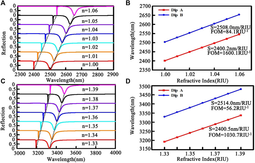
FIGURE 7. Sensing performance of the proposed step-shaped grating. Reflection spectra evolution with environmental IR (A) from 1.01 to 1.06, (C) from 1.33 to 1.39. Dependence of extracted resonant wavelengths of the two reflection dips on environmental IR (B) from 1.00 to 1.06, and (D) from 1.33 to 1.38.
Considering most chemical and biological sensors need to detect IR of a solution, we also investigated the grating sensor performance working in a solution environment. The whole device is immersed in a solution with a IR of n = 1.33 and Figure 7C is the simulated reflection spectra. As the ambient IR changes from 1.33 to 1.39, the two reflection dips still have an obvious shift and the maximal absorption still can reach near unity. Similar to working in a gas environment, the electromagnetic field is still trapped in the ambient solution above the Au grating or in the grating grooves. Therefore, this structure should still possess high sensitivity to the ambient IR change, which reach 2400.5 nm/RIU and 2514.0 nm/RIU for mode A and mode B, respectively. Figure 7D plots the reflection dips wavelength as functions of the ambient IR, it is seen that the ideal linear relationship still persists. Compared to the detection in air environments, the sensor sensitivity does not display obvious decrease. However, due to a little increase of the FWHM in the solution environments, the value of FOM slightly decreases. The specific values of the FOM for mode A and mode B are 1030.7 RIU−1 and 56.2 RIU−1.
For a direct comparison, the sensor performance (sensitivities, linewidths, FOMs and RI range) of some previously reported plasmonic nanostructure sensors [19,20,24–26,28,35,37–39] are summarized in Table 1. Obviously, the sensitivity and FOM as well as the RI range of mode A in our proposed step-shaped grating sensor outperform most previous studies. As for mode B, though the introduction of the cavity mode resonance results in a widened resonant linewidth, its FOM is not as high as that of mode A, it is still larger than many previous studies [35,37–39]. In addition, the sensitivity of mode B is even larger than that of mode A. More importantly, when the two dips work together, the modulation performance of this dual-wavelength sensor exceeds all the previous studies.
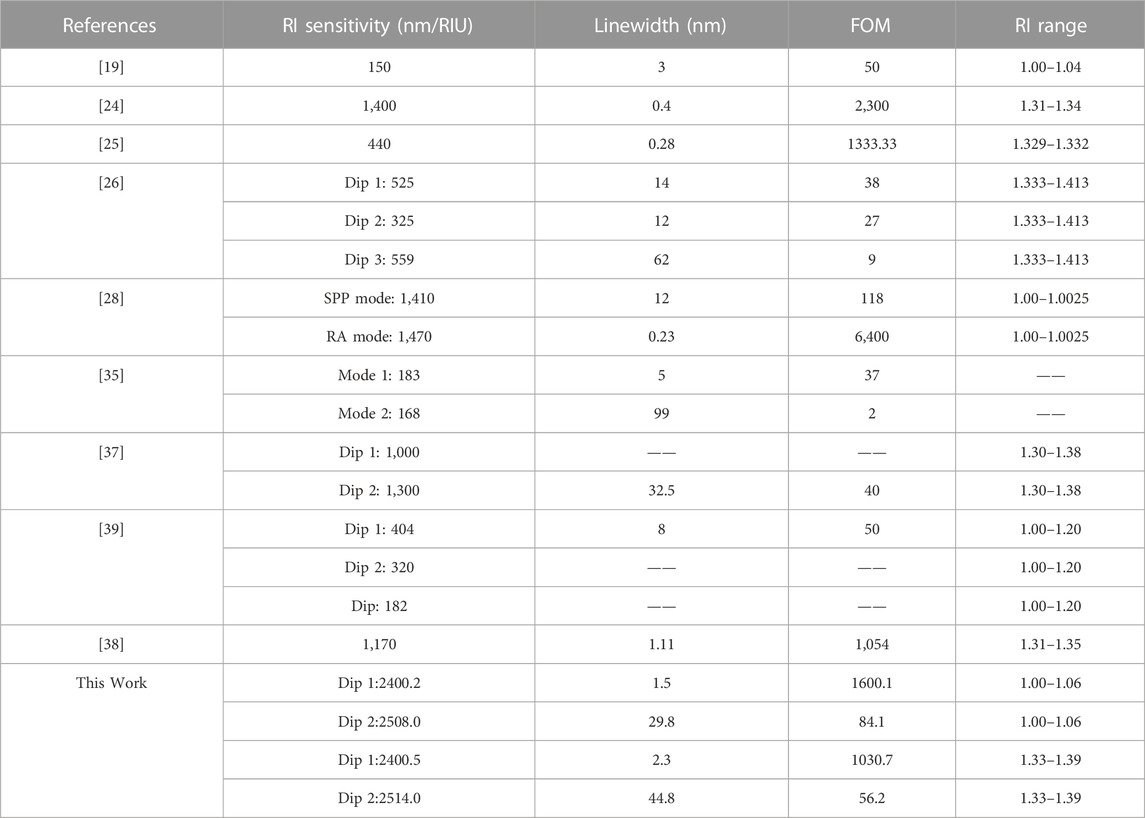
TABLE 1. Comparison of the sensing performances of plasmonic nanostructure sensors.
4 Conclusion
Based on the interaction between two diffraction coupled SPP modes, we have realized a narrowband and broadband coexisting perfect absorption effect in a simple step-shaped Au grating. The linewidth of the narrower absorption band is as small as 1.5 nm, and can be further optimized even to sub-nanometer. The linewidth of the broader absorption is tens of nanometer which is also smaller than most plasmonic resonances. The positions of the two absorption peaks can be adjusted flexibly. The two absorption peaks can both work as sensors for IR, and their sensitivities can reach over 2,000 nm/RIU without sacrificing their absorption. Unlike conventional plasmonic absorbers utilizing MIM structures, our absorber consists solely of single-layer metal, which can be easily fabricated using only one process of focused ion beam etching. As an alternative, to reduce the costs, indirect preparation methods such as electron beam grayscale exposure technology can also be used to first produce its reverse structure and through several processing procedures finally obtain the desired structure. In production, the thickness of the substrate does not need to be several hundred nanometers, slightly thicker than its skin depth is feasible in practice. Besides, other conventional metal materials such as Al can be used to replace the noble metal Au, and the similar absorption properties and sensing performances are still available. Therefore, our structure has great potential in versatile biological and chemical sensing.
Data availability statement
The original contributions presented in the study are included in the article/Supplementary Material, further inquiries can be directed to the corresponding authors.
Author contributions
ZF proposed the structural design of the absorber. JW and ZZ conducted all the simulation works. ZL and HTL produced all the figures in this article. HG conducted the physical mechanism analysis and HFL conducted the sensing performance analysis. All authors contributed to the article and approved the submitted version.
Funding
This research was supported by the National Natural Science Foundation of China (11504336).
Conflict of interest
Author HFL was employed by Beijing Huairou Instruments and Sensors Co., Ltd.
The remaining authors declare that the research was conducted in the absence of any commercial or financial relationships that could be construed as a potential conflict of interest.
Publisher’s note
All claims expressed in this article are solely those of the authors and do not necessarily represent those of their affiliated organizations, or those of the publisher, the editors and the reviewers. Any product that may be evaluated in this article, or claim that may be made by its manufacturer, is not guaranteed or endorsed by the publisher.
References
1. Atwater HA, Polman A. Plasmonics for improved photovoltaic devices. Nat Mater (2010) 9(3):205–13. doi:10.1038/nmat2629
2. Cheng C-W, Abbas MN, Chiu C-W, Lai K-T, Shih M-H, Chang Y-C. Wide-angle polarization independent infrared broadband absorbers based on metallic multi-sized disk arrays. Opt Express (2012) 20(9):10376–81. doi:10.1364/oe.20.010376
3. Zhou L, Tan Y, Ji D, Zhu B, Zhang P, Xu J, et al. Self-assembly of highly efficient, broadband plasmonic absorbers for solar steam generation. Sci Adv (2016) 2(4):e1501227. doi:10.1126/sciadv.1501227
4. Laroche M, Carminati R, Greffet J-J. Near-field thermophotovoltaic energy conversion. J Appl Phys (2006) 100(6):063704. doi:10.1063/1.2234560
5. Wu C, Neuner B, John J, Milder A, Zollars B, Savoy S, et al. Metamaterial-based integrated plasmonic absorber/emitter for solar thermo-photovoltaic systems. J Opt (2012) 14(2):024005. doi:10.1088/2040-8978/14/2/024005
6. Kim S-J, Choi H-K, Lee H, Hong S-H. Solution-processable nanocrystal-based broadband Fabry–Perot absorber for reflective vivid color generation. ACS Appl Mater Inter (2019) 11(7):7280–7. doi:10.1021/acsami.8b19157
7. Pendry JB, Schurig D, Smith DR. Controlling electromagnetic fields. Science (2006) 312(5781):1780–2. doi:10.1126/science.1125907
8. Chandra S, Franklin D, Cozart J, Safaei A, Chanda D. Adaptive multispectral infrared camouflage. Acs Photon (2018) 5(11):4513–9. doi:10.1021/acsphotonics.8b00972
9. Liu N, Mesch M, Weiss T, Hentschel M, Giessen H. Infrared perfect absorber and its application as plasmonic sensor. Nano Lett (2010) 10(7):2342–8. doi:10.1021/nl9041033
10. Reinhard B, Schmitt KM, Wollrab V, Neu J, Beigang R, Rahm M. Metamaterial near-field sensor for deep-subwavelength thickness measurements and sensitive refractometry in the terahertz frequency range. Appl Phys Lett (2012) 100(22):221101. doi:10.1063/1.4722801
11. Yong Z, Zhang S, Gong C, He S. Narrow band perfect absorber for maximum localized magnetic and electric field enhancement and sensing applications. Sci Rep (2016) 6(1):24063. doi:10.1038/srep24063
12. Cui Y, Fung KH, Xu J, Ma H, Jin Y, He S, et al. Ultrabroadband light absorption by a sawtooth anisotropic metamaterial slab. Nano Lett (2012) 12(3):1443–7. doi:10.1021/nl204118h
13. Ding F, Cui Y, Ge X, Jin Y, He S. Ultra-broadband microwave metamaterial absorber. Appl Phys Lett (2012) 100(10):103506. doi:10.1063/1.3692178
14. Zhang M, Fang J, Zhang F, Chen J, Yu H. Ultra-narrow band perfect absorbers based on Fano resonance in MIM metamaterials. Opt Commun (2017) 405:216–21. doi:10.1016/j.optcom.2017.07.007
15. Kim S, Hong D, Sattorov M, Kim S, Yoo YJ, Park SY, et al. Full manipulation of transparency and absorption through direct tuning of dark modes in high-Q Fano metamaterials. Opt Express (2022) 30(3):3443–54. doi:10.1364/oe.449968
16. Liu N, Langguth L, Weiss T, Kästel J, Fleischhauer M, Pfau T, et al. Plasmonic analogue of electromagnetically induced transparency at the Drude damping limit. Nat Mater (2009) 8(9):758–62. doi:10.1038/nmat2495
17. Wang T, Zhang Y, Hong Z, Han Z. Analogue of electromagnetically induced transparency in integrated plasmonics with radiative and subradiant resonators. Opt Express (2014) 22(18):21529–34. doi:10.1364/oe.22.021529
18. Nie J, Yu J, Liu W, Yu T, Gao P. Ultra-narrowband perfect absorption of monolayer two-dimensional materials enabled by all-dielectric subwavelength gratings. Opt Express (2020) 28(26):38592–602. doi:10.1364/oe.413032
19. Yan Z, Zhu Q, Wan M, Lu X, Pu X, Tang C, et al. Graphene ultraviolet ultrahigh-Q perfect absorption for nanoscale optical sensing. Opt Express (2020) 28(5):6095–101. doi:10.1364/oe.385658
20. Li Z, Butun S, Aydin K. Ultranarrow band absorbers based on surface lattice resonances in nanostructured metal surfaces. ACS Nano (2014) 8(8):8242–8. doi:10.1021/nn502617t
21. Kravets VG, Kabashin AV, Barnes WL, Grigorenko AN. Plasmonic surface lattice resonances: a review of properties and applications. Chem Rev (2018) 118(12):5912–51. doi:10.1021/acs.chemrev.8b00243
22. Wu F, Liu D, Xiao S. Bandwidth-tunable near-infrared perfect absorption of graphene in a compound grating waveguide structure supporting quasi-bound states in the continuum. Opt Express (2021) 29(25):41975–89. doi:10.1364/oe.446270
23. Fang X, Xiong L, Shi J, Li G. High-Q quadrupolar plasmonic lattice resonances in horizontal metal–insulator–metal gratings. Opt Lett (2021) 46(7):1546–9. doi:10.1364/ol.419364
24. Meng L, Zhao D, Ruan Z, Li Q, Yang Y, Qiu M. Optimized grating as an ultra-narrow band absorber or plasmonic sensor. Opt Lett (2014) 39(5):1137–40. doi:10.1364/ol.39.001137
25. Feng A, Yu Z, Sun X. Ultranarrow-band metagrating absorbers for sensing and modulation. Opt Express (2018) 26(22):28197–205. doi:10.1364/oe.26.028197
26. Li G, Shen Y, Xiao G, Jin C. Double-layered metal grating for high-performance refractive index sensing. Opt Express (2015) 23(7):8995–9003. doi:10.1364/oe.23.008995
27. Lu H, Liu X, Mao D, Wang G. Plasmonic nanosensor based on Fano resonance in waveguide-coupled resonators. Opt Lett (2012) 37(18):3780–2. doi:10.1364/ol.37.003780
28. Chen C, Wang G, Zhang Z, Zhang K. Dual narrow-band absorber based on metal–insulator–metal configuration for refractive index sensing. Opt Express (2018) 43(15):3630–3. doi:10.1364/ol.43.003630
30. Collin S, Pardo F, Teissier R, Pelouard J-L. Horizontal and vertical surface resonances in transmission metallic gratings. J Opt A: Pure Appl Opt (2002) 4(5):S154–60. doi:10.1088/1464-4258/4/5/364
31. Crouse D, Keshavareddy P. Role of optical and surface plasmon modes in enhanced transmission and applications. Opt Express (2005) 13(20):7760–71. doi:10.1364/opex.13.007760
32. Wood RW. On a remarkable case of uneven distribution of light in a diffraction grating spectrum. Lond Edinb Dublin Phil Mag J Sci (1902) 4(21):269–75. doi:10.1088/1478-7814/18/1/325
33. Skigin DC, Depine RA. Transmission resonances of metallic compound gratings with subwavelength slits. Phys Rev Lett (2005) 95(21):217402. doi:10.1103/physrevlett.95.217402
34. Hibbins AP, Hooper IR, Lockyear MJ, Sambles JR. Microwave transmission of a compound metal grating. Phys Rev Lett (2006) 96(25):257402. doi:10.1103/physrevlett.96.257402
35. Vala M, Ertsgaard CT, Wittenberg NJ, Oh S-H. Plasmonic sensing on symmetric nanohole arrays supporting high-Q hybrid modes and reflection geometry. ACS Sensors (2019) 4(12):3265–74. doi:10.1021/acssensors.9b01780
36. Chen Q, Liang L, Zheng Q, Zhang Y, Wen L. On-chip readout plasmonic mid-IR gas sensor. Opto-electron Adv (2020) 3(7):190040–1. doi:10.29026/oea.2020.190040
37. Chen J, Fan W, Zhang T, Tang C, Chen X, Wu J, et al. Engineering the magnetic plasmon resonances of metamaterials for high-quality sensing. Opt Express (2017) 25(4):3675–81. doi:10.1364/oe.25.003675
38. Luo S, Zhao J, Zuo D, Wang X. Perfect narrow band absorber for sensing applications. Opt Express (2016) 24(9):9288–94. doi:10.1364/oe.24.009288
Keywords: perfect absorber, ultra-narrow band absorption, step-shaped all-metal grating, diffraction coupled surface plasmon polariton, sensing performance
Citation: Wang J, Zhang Z, Lin Z, Li H, Gao H, Fan Z and Liu H (2023) Tunable narrowband and broadband coexisting absorber enabled by a simple all-metal grating for sensing applications. Front. Phys. 11:1234275. doi: 10.3389/fphy.2023.1234275
Received: 04 June 2023; Accepted: 03 August 2023;
Published: 16 August 2023.
Edited by:
Gagan Kumar, Indian Institute of Technology Guwahati, IndiaReviewed by:
Jitendra Prajapati, Shiv Nadar University, IndiaLong Wen, Jinan University, China
Jagan Mohan Rao S., Ulsan National Institute of Science and Technology, Republic of Korea
Copyright © 2023 Wang, Zhang, Lin, Li, Gao, Fan and Liu. This is an open-access article distributed under the terms of the Creative Commons Attribution License (CC BY). The use, distribution or reproduction in other forums is permitted, provided the original author(s) and the copyright owner(s) are credited and that the original publication in this journal is cited, in accordance with accepted academic practice. No use, distribution or reproduction is permitted which does not comply with these terms.
*Correspondence: Zhenjun Fan, ZmFuempAY3VnYi5lZHUuY24=; Haifeng Liu, bGl1aGFpZmVuZ0BzZW1pLmFjLmNu