 Houzhi Fei
 Dandan Sang
 Liangrui Zou1
 Cong Wang
 Qinglin Wang
- 1Shandong Key Laboratory of Optical Communication Science and Technology, School of Physics Science and Information Technology, Liaocheng University, Liaocheng, China
- 2Shandong Liaocheng Laixin Powder Materials Science and Technology Co., Ltd., Liaocheng, China
- 3College of Mathematics and Physics, Beijing University of Chemical Technology, Beijing, China
Diamond has a variety of unique characteristics, including integrates mechanics, electricity, heat, optics and other excellent properties, so that it is widely focus on the field of high and new technology, especially in the optoelectronic technology. Because diamond has the characteristics of high thermal conductivity, high breakdown field (10 mV/cm), high electron and hole mobility, it has a wide application prospect in high temperature, high power and high frequency photoelectric equipment. The wide bandgap (5.47 eV) makes diamond an ideal material in ultraviolet detectors (UV). Its high carrier mobility and breakdown field strength make it an ideal choice for field emission materials, which are expected to be used in high-power electronic devices in the next few years. At the same time, in addition to high hardness, it also has various of excellent physical properties, such as low coefficient of thermal expansion, low coefficient of friction, high acoustic propagation speed and high optical transmittance, so that it has broad application prospects in many fields such as machining, microelectronic devices, optical windows and surface coatings. In addition, diamond also has a high exciton binding energy (80 meV), which plays an important development in deep ultraviolet and high-energy particle detectors. In this article, the latest progress in the application of diamond-based optoelectronic devices is reviewed. A variety of advanced devices and physical phenomena are considered, for example, sensors, transistors, memory, Light-emitting diode (LEDs), ultraviolet detectors and field emission. This review will provide a new idea to promote the development of photoelectric applications based on diamond structure.
1 Introduction
Diamond has been recognized as one of the most promising materials for next-generation power electronics and optoelectronics devices because of its rich properties and attractive semiconductor properties. Diamond has many excellent physical and electrical properties. It is the hardest substance on Earth, with a high density, high melting point, extremely high thermal conductivity, and excellent corrosion resistance. At the same time, its insulation, wide forbidden bandwidth, high breakdown field strength, high electron mobility and high band migration make it promising in the field of optoelectronic devices. It can well overcome the limitations of typical previous generation semiconductor devices [1, 2]. Among them, because of its ultra-wide band gap, the ultraviolet detector using diamond structure has great spectral response and strong visible light blindness in the ultraviolet part shorter than 230 nm. Moreover, diamond structures in various forms (e.g., graphene/diamond heterojunction, hydrogen-terminated diamond (diamond: H), diamond Island wafer (DIW)) have been manufactured for various applications, including transistors [1], photoelectric storage [3], fiber optic sensors [4], light-emitting diodes [5], cathode field emission [6], and ultraviolet detectors [7]. So far, diamond structures have been combined with a variety of materials and dopants to manufacture optical and electronic devices, including B [8], Ti and Al [9]. However, to date, there has been no comprehensive discussion focusing particularly on diamond related material of optoelectronic device applications. In this review, we summarize the past research progress of diamond materials in various devices and applications, including field emission, sensors, memory, light-emitting diodes (LEDs), transistors, and ultraviolet detectors. From the current research progress, we put forward the existing problems and prospects in the research field of diamond-based optoelectronic devices, it provides theoretical basis and effective guidance for promoting the application and development of diamond related optoelectronic devices.
2 Field emission
Over the past few decades, diamond has attracted considerable interest as an alternative to conducting metals and semiconductor cold cathodes [10]. Diamond films exhibit stable planar electron emission characteristics under low electric field conditions because of their negative electron affinity, strong bonding structure, extreme hardness against nanomaterials, ion bombardment resistance and good thermal and electrical conductivity [11]. The researchers usually by looking for current density as a function of applied electric field to evaluate the field emission properties [12]. However, due to its lack of high conductivity, its potential application in electron emission devices is limited. However, p - or N-type dopants improve the situation [13]. For the sake of perfect the field emission properties of the films, Zhang et al. [6] sputtered metal Ni, Al, Mo, Ti on the diamond surface, and compared the field emission properties of various diamond/metal compound films. The prepared diamond film is uniform and the density of diamond particles is higher. They used DC magnetron sputtering equipment to sputter metal Ti, Al, Mo and Ni layers diamond film with high nucleation density, and deposited them on the diamond surface, forming metal-semiconductor contact interface on the diamond surface. It is known from the experimental data that depositing thin metal layers is a good way to reduce the effective work function, with the Ti metal layer playing the most significant role. Therefore, diamond/titanium composite films have good field emission performance, which has potential value in field emission flat panel displays and other electronic source applications. Chen et al. [14] improved the electron field emission (EFE) characteristics of UNCD films by undoped low pressure annealing. By increasing the annealing temperature to 900–1,000°C, they found that the conduction field of UNCD films decreased from 5.8 V/μm to 1.3 V/μm and then to 0.8 V/μm, the current density increases significantly to 7180 μA/cm2 at 1.3 V/μm and 3180 μA/cm2 at 0.8 V/μm. The films annealed at 900–1,000°C have good EFE properties. However, when the annealing temperature is further increased to 1,100–1,200°C, due to the high temperature of silica in the annealing chamber, silicon-oxygen bonds may be formed during the annealing process. They confirmed the existence of silicon-oxygen bonds based on the atomic ratios calculated from the XPS results. The silico-oxygen bond has a negative effect on the conductivity due to its insulation, resulting in the EFE property of the film completely disappearing. HRTEM (Figures 1A–F) and Raman (Figures 1G, H) spectroscopy results showed that annealed diamond particles were smaller and had fewer defects, resulting in continuously conducting graphene nanoribbons (GNRS), which also effectively improved EFE performance. This study provides a new prospect for the application of UNCD film based cold cathode emission devices. Ee Le Shim et al. [8] used AFM and SEM to observe the morphology of nano-diamond (BND) and Boron-doped Microcrystalline Diamond (BMD), and used MA-CVD to grow the films on Si substrates. By measuring the emission characteristics of BMD film and its corresponding BND film, the I-V diagram and F-N diagram analysis showed that BND was superior to BMD as a field emitter. Meanwhile, the long-term current stability of BND and BMD was measured and compared, discover BND is a more stable current emitter.
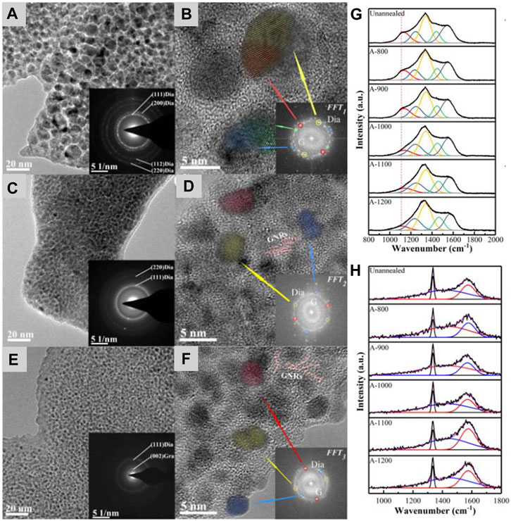
FIGURE 1. HRTEM image. (A) unannealed, (C) annealed at 900°C, (E) annealed at 1200°C. Illustration is SAED pattern. (B, D, F) Microstructure of HRTEM images obtained from the above three samples, illustrated in FFT mode. (G): Raman spectra fitted for all samples under 514 nm visible light excitation. (H): Raman spectra of all samples excited by 244 nm ultraviolet light.
Carbon nanowalls (CNWS) are vertically aligned nanostructures. Huang et al. [15] prepared CNWS by MPCVD method, and then modified ultra-nano diamond particles to improve field emission efficiency and stability. They control the high uniformity of nanodiamond density by using electrostatic self-assembly seed technology. The results of TEM, Raman spectroscopy, XPS and XRD show that the structure order and crystallinity of sp2 phase decrease and the ratio of sp3/sp2 increases for the diamond modified CNW prepared after the dispersion and short-term growth in MPCVD. In other words, the field emission efficiency of diamond-modified CNW is significantly improved, and the open field is reduced to 1.8 V/μm−1, which is entirely due to the greater field amplification. Ficek et al. [16] prepared edge-rich diamond-reinforced carbon nanowalls (D-ECNWs) and obtained excellent field electron emission (FEE) characteristics. The morphology and conductivity of D-ECNW observed by them through C-AFM are shown in Figures 2A, B. AFM measurements (illustration) indicate that the typical thickness of a single D-ECNW is less than 100 nm. By applying an applied electric field of 5.5 V μm−1, the structure was measured to have a low E0 value of 3.1 V μm−1 and a high Je of 2.6 mA cm−2 (Figure 2C). The illustration reveals the lifetime stability of the FEE with this structure. It can be seen from the slope of Figure 2D that the D-ECNW nanostructure also has a large β value. Figure 2E shows that the D-ECNW nanostructure as a cathode can ignite plasma at a low voltage of 330 V. Furthermore, when the applied electric field is 5000 V cm−1 (applied voltage is 500 V), the JPI reaches 1.2 mA cm−2 (Figure 2F). This study confirms that D-ECNWs has good properties under low threshold voltage and high ionization stability, and can be used as the cathode of microplasma devices.
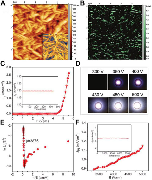
FIGURE 2. (A) Top view of the D-ECNW surface. (B) C-AFM cantilever beam (current logarithm I/V converter) image. (C) Function of emission current density (Je) and applied magnetic field I (the illustration shows the Je curve with respect to time, i.e., the FEE lifetime stability of the structure). (D) F-N diagram corresponding to the e-E characteristic curve. (E) Lighting characteristics of plasma. (F) Plasma current density in a microplasma cavity in relation to the applied field (illustration showing the plasma irradiated lifetime stability of these nanostructures) [16].
Sonali et al. [9] explored CVD diamond films and ZnO nanoneedles. They studied the relationship between emission current density and applied voltage and found that as the applied voltage increased, the emission current density increased faster. It is the negative electron affinity of CVD diamond that promotes electron tunneling through the ZnO-CVD diamond heterojunction, resulting in a faster increase in emission current density and better emission characteristics. The above results show that it is the joint action of diamond microcrystals and ZnO nanoneedles that makes the field emission characteristics of ZnO nanoneedles on CVD diamond surface better. Zhang et al. [17] first observed SEM images of diamond film at different magnification discover the diamond film is fine and uniform. By comparing AFM images of diamond film and diamond film deposited on Ti layer, they excluded the influence of surface topography changes on field emission characteristics. They carried out the electron emission of the simple film and found that the diamond/titanium composite film exhibited higher emission current characteristics. The conduction field is about 3V/µm and can reach 1400 μA/cm2 at 25 V/µm. Therefore, the diamond/titanium composite film has potential application value for field emission flat panel display and other electronic source applications. Li et al. [18] used two different deposition temperatures to grow diamond-graphite nanohybrid films, and found that microstructure and appearance of films changed significantly when the deposition temperature increased from 730°C to 830°C. The first film obtained is named DGN730, and the second film is named DGN830. Their electron field emission characteristics were measured (Figures 3A, B), and it was found that the emission current density of DGN830 film was 1.6 mA cm−2 when the electric field of 9.9 V was applied, which was 8 times that of DGN730 film. Therefore, the electron field emission on the DGN830 membrane is significantly enhanced. This study provides an ordinary method to effectively change the microstructure of sp2/sp3 nanohybrid films, which is extremely beneficial for the development of carbon based field emission cold cathodes with good function. Kolekar et al. [19] observed homogeneous nanodiamond films using scanning electron microscopy, and comparing these images with AFM images, it is found that only a few ND clusters contribute to field electron emission. The I-V measurement by C-AFM shows that the film has high insulation and can be used as a gate electrode in FET. The ln (J) vs. (1/E) plots showed a good linear relationship and the main mechanism of electron emission is F-N tunneling. Therefore, the results of the field emission microscope are very important in the potential application of ND as a field transmitter. For high brightness photocathodes operated by ultra-fast laser triggered laser, the tungsten tip of ND coating also has great application potential.
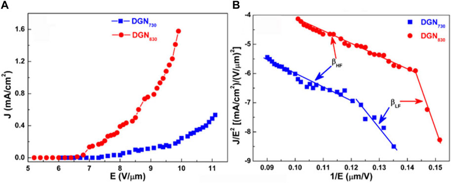
FIGURE 3. (A) is the E vs. J characteristic curve of different films. (B) is the corresponding Fowler-Nordheim graph (Je/E2 vs. 1/E curve) [18].
3 Sensor
Diamond is considered the ultimate material for semiconductors used in power electronics applications, with advantages over other wide-gap semiconductors [20]. For example: high electron drift rate, high bandgap energy and high electron saturation drift velocity. Sensor made using diamond have at least three times the radiation resistance, at least two times the charge collection and four times the thermal conductivity of their silicon counterparts, making them attractive materials for applications in new sensor [21]. At the same time, diamond has a promising prospect in the application of biochemical sensors because of its special chemical and mechanical properties [22]. Kosowska et al. [4] have studied the reflection applications of boron-doped NCD and nitrogen-doped NCD on the surface of doped nano-diamond (NCD) films, and built refractive index interference sensor for liquid measurement. They built an optical fiber device to measure the refractive index of the sample on the basis of Fabry-Perot interferometer (Figure 4A). Two will be used in this experiment superlight-emitting diodes operating at the central wavelength of 1290nm and 1560 nm respectively. The spectral separation between the refractive index and the maximum value was measured (Figures 4B–E), and the correlation coefficient R2 and sensitivity values of the sensors operating at 1290 nm and 1560 nm were calculated and determined. It is found that the R2 value achieved is in the range of 0.7–0.9 and some are greater than 0.9. There is a high negative correlation between the refractive index value of the fringe and the spectral resolution. This method ensures better chemical and chemical resistance to mechanical damage, extends the life of the sensor, and allows measurement of biological samples and corrosive chemicals.
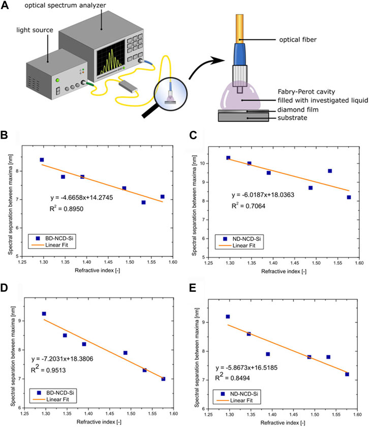
FIGURE 4. (A) Indicates the image of the measurement setup and a close measuring head. (B) The measurement results are shown: when the wavelength is 1,290 nm, the extreme value of spectral separation is used as a function of refractive index BD-NCD-Si. (C) The measurement results are shown: when the wavelength is 1,290 nm, the extreme value of spectral separation is used as a function of refractive index ND-NCD-Si. (D) The measurement results are shown: when the wavelength is 1,560 nm, the extreme value of spectral separation is used as a function of refractive index BD-NCIi. (E) The measurement results are shown: when the wavelength is 1,560 nm, the extreme value of spectral separation is used as a function of refractive index ND-NCD-Si [4].
Shen et al. [23] proposed the use of fluorine, hydrogen, nitrogen and oxygen terminated diamond (110) surfaces for nitrogen vacancy (NV) centers and studied their properties. Using density functional theory, they calculated that diamond (110) has interband states and surface electron spins on the surface of the oxygen sealing surface, interband states on the nitrogen sealing surface, and negative electron affinity on the hydrogen sealing surface. Therefore, they consider these three surfaces inappropriate. Fluorine sealed diamond (110) has a positron affinity, no surface-dependent band gap states, and no surface electron spin, so this is very promising for NV-based quantum sensors. Bahr et al. [24] designed and tested an integrated magnetic sensor that can only be accessed and read optically. Using this device, they found a non-optimal magnetic sensitivity of about 48 nA μT−1 in a DC magnetic field. In sensitive measurement environments, it can be easily integrated compared to other small sensor devices. Liu et al. [25] used nitrogen vacancy (NV) centers in diamond as quantum sensors to detect NMR signals. They first prepared alumina layers by depositing atomic layers, then chemically functionalized them with phosphates to form self-assembled monolayers. Surface NV-NMR techniques detect spatially resolved NMR signals from monolayers. In this way, they demonstrated that the NV quantum sensor is a surface-sensitive NMR tool with femtosecond sensitivity that can be used for in situ analysis in catalysis, materials and biological studies. This approach offers the advantages of NMR spectroscopy being non-invasive, and its functionality and low technical complexity in chemically relevant conditions also make it a practical technique for catalysis, materials science, biosensing, or two-dimensional materials research.
Salvatori et al. [26] deposited polycrystalline diamond films on silicon substrates by CVD and used them as thin films of pressure sensors by selective chemical etching of silicon (SEM diagram is shown in Figure 5A). They assessed the pressure by measuring the cavity length with an electro-optical system coupled to a single-mode fiber. When the pressure applied to the diamond film is compressed towards the fiber plane, the cavity length will decrease ∆d (Figure 5B). The photocurrent data of a film with a diameter of 360 μm at 430 kPa pressure is shown in Figure 5C, which is found to be proportional to the incident light power of PD. The repeatability of the sensor was also evaluated through several 0–300 kPa cycles (Figure 5D). Figure 5E shows the simulation of A2/A1 light intensity ratio with different values. When the A2/A1 ratio is greater than 0.8, the failure interference between beams produces a steeper response. Conversely, low-dynamic “sinusoidal” behavior occurs when the intensity ratio is below 0.4. The measurement results of samples with a membrane diameter of 380 ± 20 m under the pressure range of 0–3 MPa are shown in Figure 5F. The data observed when the minimum signal was given are collated in Figure 5G, where pretty good linear relationship is found over the study area. The sensor structure has been proved to be feasible through various measurements through, the proposed sensor system solves the problem better than the traditional solution and solves the shortcoming of electromagnetic interference caused by the tiny signal obtained by the standard piezoelectric sensor. Pettinato et al. [27] designed and tested a pressure sensor based on diamond films that can be used to measure gas pressures up to 6.8 MPa (part of the structure is shown in Figure 6A. As can be seen from Figure 6B, on the vertical axis, the displacement values normalized according to the applied pressure are displayed, in this case these values are consistent with the sensitivity of the sensor. Figure 6C shows preliminary results of diamond film samples with diameters of (400 ± 10) μm in the pressure range of 0–3.6 MPa, confirming the expected sinusoidal behavior. The dashed lines represent the best results fitted according to the above formula and are very consistent with the reported values for this diamond. Figure 6D highlights the diaphragm curvature at the center position and shows the simulation results of diaphragm displacement per unit of pressure. Figure 6E is the result of another sensor with a membrane diameter of (350 ± 10) μm. This measurement highlights the amplitude of the interference signal so that monotonic behaviour below 0.5 MPa can be well observed. They also systematically studied several membrane samples of different diameters. The new sensor is resistant to electromagnetic interference and can be used in harsh environments. Zhang et al. used H-type diamond as raw material and obtained part of O-type diamond by ultraviolet ozone treatment [28]. Then the diamond surface is modified, and finally the glucose concentration is determined by the displacement of the transfer characteristics. The biosensor has a wide linear response in the range of 10–5 to 10–1 M, with a sensitivity of −53 mV/log10 [glucose concentration]. At the same time, the sensor has good repeatability and stability through many experiments. Their proposed partial O-diamond biosensor could be an effective solution for glucose detection.
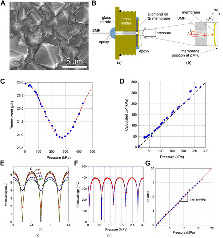
FIGURE 5. (A) SEM image of silicon surface of polycrystalline diamond film with thickness of 5.9 μm. (B) The left is the schematic diagram of sensor structure. (C) Photocurrent signals are obtained for films with a diameter of 360 μm at pressures up to 430 kPa. (D) The repeatability of the sensor is evaluated at several 0–300 kPaIcles. (E) The output signal of PD optical voltage is normalized as a function of the wavelength of incident light with the length of FP cavity under different A2/A1 intensity ratio of reflected beam. (F) Indicates the diameter of 380 μm the relationship between PD photovoltage output signal and pressure difference of PCD film. (G) For PCD film with a diameter of 380 μm, when the minimum value of the measured signal is 16.5 MPa, the film deflection is evaluated as a function of the pressure difference [26].
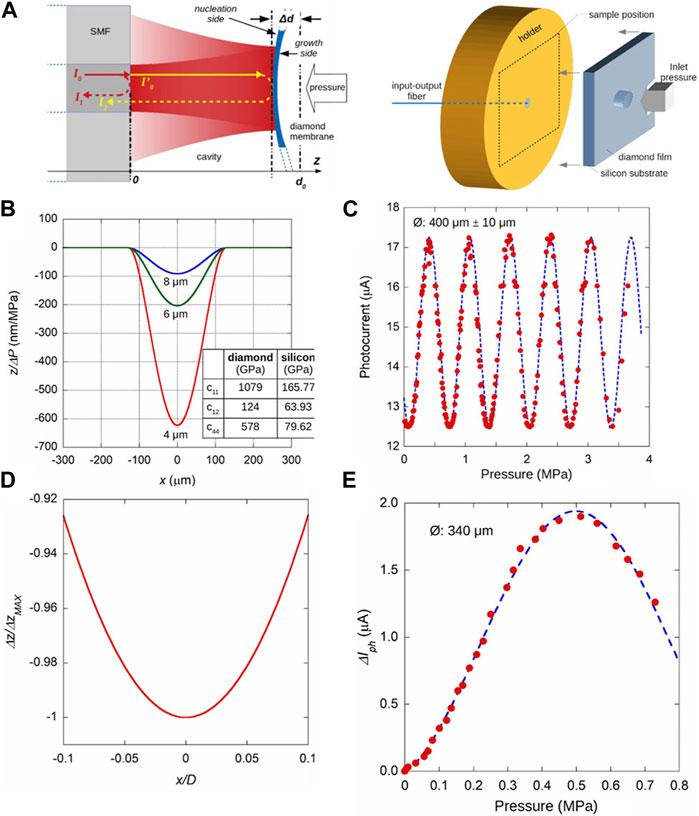
FIGURE 6. (A) Schematic diagram of sensor FP cavity structure and schematic diagram of sensor element structure. The cavity length is equal to the thickness of the silicon substrate. (B) Numerical calculations representing the normalization of deflection and inlet pressure for diamond films with diameters of 250 μm and thicknesses of 4, 6 and 8 μm. (C) represents the photocurrent signal obtained by a membrane with a diameter of about 400 μm at a pressure up to 3.6 MPa. (D) is the simulation normalized to the maximum displacement per unit pressure as a function of the normalization of the x position of the membrane Imeter D. (E) represents that for a membrane sensor with a diameter of about 350 µm, the variation of photocurrent amplitude with the obtained value at p = 0 is a function of the inlet pressure [27].
Guthoff et al. [29] discussed polycrystalline (pCVD) diamond sensors and silicon (Si) sensors. For the sake of measure the more durable stability and nonlinearity of the sensor, at the beginning and end of each LHC filling, perform a quick calibration scan in the nominal operation to obtain the calibration constant бvis. They investigated the respectively бvis in two different sensor as a function of the single beam instantaneous brightness (SBIL). The results show that the pCVD diamond sensor has higher reliability than the sCVD diamond sensor under high rate environment. The disadvantage of low charge collection does not indicate a problem. A slight nonlinearity was observed, and the efficiency of the peak luminosity was reduced by about 2%–3% compared to late stages of a typical LHC fill. The prototype silicon diode sensor shows good linearity. Belwanshi et al. [30] used the finite element simulation method to study the sensor response of silicon micromechanical membrane and diamond or silicon carbide oxide isolation piezoresistance. They first compared the output voltage change and input pressure of Wheatstone bridge of pressure sensor of silicon diaphragm with different piezoresistive materials, and found that SiC or diamond based piezoelectric resistor is combined on silicon diaphragm, and its sensitivity is 14 and 166 times lower than that of silicon piezoelectric resistor. They found that the stress of the silicon diaphragm is the highest and that of the diamond diaphragm is the lowest under the specific pressure. And increase in sensitivity if the diaphragm and piezoelectric resistor are made of SiC or diamond material. Their research provides a new idea for the development of pressure sensors in harsh environments.
4 Memory application
Quantum optical memory (QOM) is a device that can store optical quantum information and retrieve it on demand [31]. In recent years, the near-end nuclear spin of negatively charged single N-V center in diamond has become a good quantum memory for information storage [32]. In addition, single photons are challenging to create, manipulate, and measure, but are essential for a variety of quantum techniques, including cryptography, enhanced measurement, and information processing. Quantum memory will be a key supporting component for these future technologies [33]. Battistoni et al. [34] developed and studied an electronic device with memory performance based on titanic-doped CVD diamond (TiD). The characteristics of TiD samples are shown in Figures 7A, B. They evaluated the suitability of the TiD material for neuromorphic applications. The measuring device is shown in Figure 7C and found that the material performed well. Measuring the response of the device to a pulse stimulus (Figure 7D) shows that the device is able to adjust its internal conductivity when stimulated with a voltage pulse of appropriate amplitude and duration. They found that the response of the initial current to the stimulus varies depending on the polarity (Figure 7G) and pulse residence time (Figure 7F). That is, positive pulses increase the synaptic weight of the system, and negative inputs allow the system to reset back to the initial value. In addition, TiD devices exhibit some neuronal characteristics, such as the ability to store and integrate input (Figure 7E). Their research paves the way for the application of neuromorphic systems.
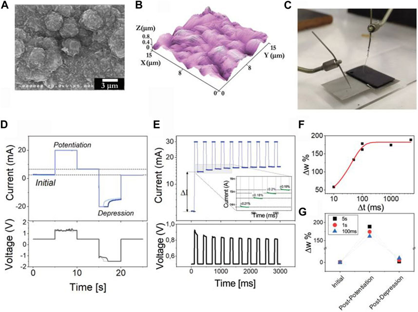
FIGURE 7. (A) SEM image of TiD; (B) 3D AFM images. (C) Image of measurement Settings. (D) Response of memristor devices (based on TiD) to enhanced and suppressed vIage pulses; (E) The response of the device to the enhanced stimulus sequence Δt = 100 ms. Illustration: The compliance used is 30 mA. (F) and (G) are the evolution of synaptic weight with pulse residence time [34].
Tuissi et al. [35] proposed a new method using shape memory alloy (SMA) as actuator based on the phenomenon of high-performance shape memory effect (HP-SME). The functional schematic diagram of HP-SME actuator and conventional SME actuator at constant pressure is shown in Figure 8A. They used a nickel-rich nickel-titanium alloy to build a diamond-like geometric device, and carried out laser processing and testing on it (Figures 8B, C), and found its good characteristics. It can be seen from Figure 8D that the thermal mechanical properties of the diamond elements treated by HP-SME are good. It is also verified that the new device has the ability to recover extremely high elongation value (about 30% of the length of the diamond) under the force of 0.7 N (Figure 8E). This provides a good idea and method for the realization of a new shape memory actuator that can work under higher working load and temperature. Ludmila et al. [36] studied the influence of diamond structure on its physical and chemical properties, and used its crystal structure to calculate the spatial sequence (The three-dimensional structures of the crystals were converted into interatomic distance histograms at a step of 0.01 Å (Figure 9A)). They estimated Hurst index H by using the DFA and PSD [Figures 9B, C are calculation examples of DFA and PSD], and found that the H values of diamond and graphite were 0.27–0.32 and 0.37–0.42, respectively. The data results show that the diamond spatial sequence has a long memory and there is a negative correlation between the sequence items. When studying the scale invariance region (Figure 9D), they found the inflection point position is related to the lattice parameters. The data obtained in this study have implications for computer-aided molecular design of new substances and materials.
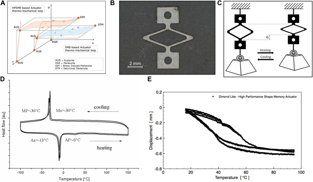
FIGURE 8. (A) Thermo-mechanical circuit diagram of the new brake. (B) Laser processing SMA diamond-like actuator. (C) Schematic diagram of diamond element under applied force. (D) DSC curve of SMA laserItting element. (E) Thermal circuit under dead load (0.7 N) [35].
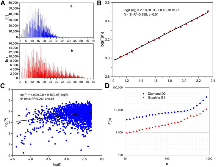
FIGURE 9. (A) Histogram of interatomic distance between diamond D2 (top) and graphite G1 (bottom). (B) Function F(n) vs. block size n for graphite G1. (C) Power spectrum of diamond D2. (D) Scale invariance region calculated from DFA data [36].
5 Light-emitting diodes
The development of electronic devices, especially those involving heterogeneous integration of materials, presents an even greater challenge in addressing their thermal operating temperature requirements [37]. Diamond has become a promising material for high power heat dissipation due to its high thermal conductivity (2200 W/mK) and low expansion coefficient [38]. The combination of diamond and LED can greatly improve the performance of LED, so that LED can be better used as a light source in chemical sensing and other field [39]. Sung et al. [5] found that diamond LEDs manufactured with various N-type dopants (such as nitrogen, lithium or phosphorus) have the problem that N-type dopants are not effective electron donors. However, they found that in the heat-treated diamond lattice, the substitution of nitrogen atoms for carbon atoms tended to leave nearby carbon atoms vacant, thus forming N-V pairs. If lithium atoms are implanted or thermally diffused into the diamond lattice, they may take up vacant positions near nitrogen atoms. Therefore, they believe that LiN pair may be a better N-type dopant for achieving diamond LED power. By depositing the cubic (B, Al) N slow-growing epitaxy on the cubic (100) surface of diamond crystal, the cubic nitride is also obtained without piezoelectricity, which provides a new idea and method for realizing the ideal LED crystal with high efficiency and high power.
Kyatam et al. [40] evaluated the effect of different circuit boards on LED lifetime. They installed high-power Cree LEDs on FR4, MCPCB and diamond circuit boards and measured the settling temperature. It was found that in the worst case, when applying 350 and 700 mA forward currents, junction temperatures with diamond would decrease by 19 and -24°C, respectively, compared to using MCPCB boards. The change of junction temperature has a great effect on the life of LED. Based on the activation energy of the aging process, they deduced that LEDs mounted on diamond boards aged 60%–90% slower than those mounted on MCPCBS at 350 mA forward current, and 90%–99% slower at 700 mA. The results show that diamond chip has broad application prospect. Chen et al. [41] investigated diamond coating as a thermal diffusion thin layer GaN LED chips. The I-V characteristic measured through the chip on both bare and diamond-coated Si substrates and it is found that the electrical properties of the chip are unaffected by the thermal diffusion layer of diamond. The temperature of the chips is also measured on both substrates and found that the maximum temperature (86.6°C) and the biggest difference in temperature (26.7°C) of the thin GaN chips Si substrate in the diamond coating were lower than those on the bare Si substrate, demonstrating that the diamond diffusion layer can improve the horizontal thermal diffusion and effectively disperse heat and achieve temperature uniformity. Under high current input, the junction temperature of a thin GaN LED with a diamond thermal diffusion layer was also 20°C lower than that of a thin Gan-LED chip with a bare silicon substrate. Xie et al. [42] proposed a new structure that can improve the modulation bandwidth of LED, and focused on the heat dissipation performance of this structure. They used COMSOL software to establish two heat dissipation models, one with diamond structure added to the new structure, and the other without it. And compare the two models. The maximum temperatures for diamond containing and diamond free structures are 356 K and 362 K, respectively. The results show that diamond structure can improve the heat dissipation performance of the device. The improvement of the heat dissipation performance also increases the upper limit of the injection current density of the LED, thus increasing the carrier concentration, reducing its composite life, and thus widening the modulation bandwidth. This study provides a favorable structure for the development of high bandwidth GaN-based LEDs.
Ke et. al [38]. studied the low nucleation density and cracking of nitrogen doped ultra nano diamond (N-UNCD) grown on InGaN based LED with concave nano pattern (CNP) structure. TEM double beam bright field (BF) captured from N-UNCD/CNP-LED samples is shown in Figure 10A). It is found that MPCVD system has excellent coverage capability on CNP-LED. However, there were many gaps between the N-UNCD and p-GaN layers, so they zoomed in on the red square in Figure 10A to further understand the growth mechanism of N-UNCD on the LED (Figure 10B). The I-V-T characteristics of Ni ohmic contact in the same plane on N-UNCD/CNP-LED are shown in Figure 10C. The linear behavior shows that Ni has good ohmic contact on N-UNCD. The schematic diagram of two carrier transmission paths is shown in Figure 10D. N-UNCD/CNP-LED exhibits a stable peak EL wavelength of about 447.1–447.3 nm in the injection current range of 10–100 mA (Figure 10E). Therefore, the blue shift of peak wavelength due to QCSE shielding is not obvious. It can be seen from Figure 10F that the emission of N-UNCD/CNP-LED is mainly radiation composite. The relief of QCSE results in a stable emission wavelength, and the radiation recombination proves that N-UNCD is an ideal conductive layer for InGaN based LEDs with CNP structure.
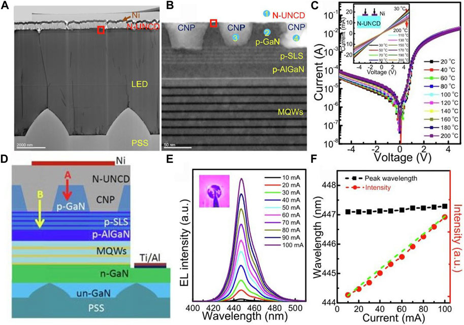
FIGURE 10. (A) TEM dual beam bright field image of Ni/N-UND/CNP-LED (profile [0 0 0 0 2]). (B) HRTEM cross-section image of N-UNCD/CNP-LED. (C) Ni/N-UND/CNP-LED I-V-T curve (Ni/N-UNI-V-T curve in the small box). (D) Possible injection current path diagram Ni/N-UND/CNP-LED. (E) EL spectrum of Ni/N-UND/CNP-LED; Illustration for CCD imaging (10 mA injection current). (F) Relationship between peak EL wavelength, integrated peak intensity and injection current of N-UNCD/CNP-LED. The green dotted line is the guide line as L approaches II [38].
6 Transistor
Diamond semiconductor has the highest room temperature thermal conductivity, high hole and electron mobility, high breakdown field and large band gap (5.47 eV) [43]. Becoming a promising material for transistors used in harsh environments [44, 45]. Diamond-based bipolar junction transistors (BJTS) offer much improved and more stable performance at high power levels [46]. In addition, diamond is an attractive material for bioelectronic systems due to its biocompatibility, chemical stability and excellent optical, mechanical and electrical properties [47]. Diamond-based solution gate field-effect transistors (SGFETs), for example, show great promise in biosensing and bioelectronics [48]. Ultra-sensitive, marker-free and sequence-specific DNA sensors have been introduced via diamond SGFET. The DNA sensor is expected to be used for electronic DNA arrays and rapid characterization of nucleic acid samples for pharmaceutical and in vivo diagnostic purposes [49]. In addition, it is possible to immobilize the aptamer PDGF on diamond SGFETs for high-resolution and marker-free potential sensing. By controlling the surface chemical properties of diamond SGFETs, the high-resolution detection of PDGF is realized [50].
Zhang et al. [51] prepared a novel hydrogen-terminated (H-terminated) diamond field effect tube containing CeB6. H-terminated diamond conduction is to use the special properties of diamond to achieve current conduction. The H-terminated diamond FET is composed of a layer of semiconductor diamond, and its surface is distributed with hydrogen atoms, which are closely connected with the crystal structure of the diamond, forming a sparse diamond, called the thin film FET, with a large gap insulation. Under the action of the thin film FET, electrons can easily enter the diamond from the surface of the diamond, because these electrons have a lower energy, and the electrons inside the diamond have a higher energy, so when the electrons enter the diamond from the surface, there will be a potential difference, resulting in a current. Its energy band diagram is shown in Figure 11A. So far, great progress has been made in the H-terminated diamond field-effect transistor (FET) with A breakdown voltage of 2 kV, a maximum oscillation frequency of 120 GHz, a power density of 3.8 W/mm, a cutoff frequency of 70 GHz, a current density above 12000 A/cm2, and a mobility of 680 cm2/V·s. They found that when the VTH is −0.46 V, the FET usually closes. The maximum drain-source current density (IDmax) is −83.8 mA/mm (Figures 11B, C show the output characteristics of the FET). The interfacial state density (Dit) is estimated to be 1.93 × 1012 cm−2·eV−1. This value may be due to the presence of pure interfaces in the grid. This study provides an effective idea for realizing normally closed H-end diamond Fets. Choi et al. [52] studied the device performance of boron-doped diamond MESFETs grown on heterogeneous epitaxial diamond substrates. Devices prepared with Lgd = 10 μm have good shear characteristics and high switching ratio (∼105), but have low Id and high Ron of 66 nA/mm at room temperature. At 463 K, the Id increases due to the decrease of resistance, but the body leakage current worsens the shear characteristics. They confirmed the breakdown characteristics and temperature of LGD. Vbr value increases with the increase of Lgd, but decreases with the increase of temperature. However, this structure will need to be modified in future processes because the electric field corresponding to Vbr is much lower than the theoretical potential of diamond.
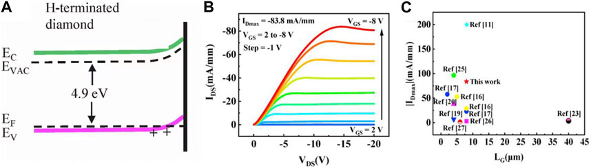
FIGURE 11. Schematic of band diagrams (A) H-terminated diamond surface. Output characteristics (B) IDS, (C) |IDmax| comparison [51].
Diamond two-dimensional hole gas has high density of hole chip, high mobility of hole and low contact resistance. P-diamond FET is an excellent candidate for realizing high temperature plasma Asia-Pacific Hertz application and far infrared devices. Shur et al. [53] evaluated the potential of diamond for terahertz (THz) and infrared plasma detection. They found through measurement that the plasma velocity is small, lower than the electron saturation velocity near the threshold, which provides an important theoretical basis for the realization of “plasma burst” instability in 2DHG. By comparing the influence of different channel lengths on the variation of basic plasma frequency with current and voltage, and taking the quality factor as a function of plasma frequency, they concluded that the plasmon resonance was stronger in the samples with better mobility, and that high migration FETs can even operate in resonant modes in the 200 GHz–300 GHz atmospheric Windows. The experimental results show that the new design and method of using diamond physics on the transistor can make the transistor have better performance, effectively improve the mobility of hole field effect, and minimize the parasitic effect. Once realized, this P-channel diamond transistor could play an important role in plasma terahertz applications in 5G communications, the Internet of Things, biomedical and sensing applications. Lundh et al. [54] evaluated the thermal performance of H-end diamond FET using the nanomin-assisted Raman temperature measurement and electrothermal device model. They measured the thermal resistance of the diamond FET in the diamond channel (about 1 mm K/W). The thermal properties of diamond Fets are compared with GaN, Al0.70Ga0.30N and β-Ga2O3 transverse transistor structures, and it is found that diamond transistors show more powerful properties. These findings show that diamond is capable of handling the higher power densities expected of UWBG-based microelectronics and provide a way to overcome current thermal barriers to realizing the full potential of UWBG-based semiconductors.
Huang et al. [55] reported the first without hydrogen seal channel diamond fin field effect transistor (diamond FinFET). They maintained effective control of channel conduction by accumulating holes in MOS structures constructed on the fins. The design and manufacture of a device with 100 nm wide fin ensures that the channel can be clipped at zero grid bias. The transmission characteristics of the FinFET show an on/off ratio greater than 3,000, successfully proving the behavior of the transistor. They also allowed the device to be characterized at room temperature and 150°C and found that the current density at 150°C was 30 mA/mm, 35 times higher than at room temperature. They report takes full advantage of the silicon industry’s fin concept and advances in diamond materials to provide a new diamond transistor for applications ranging from digital and radio frequency electronics. Syamsul et al. [56] investigated the full potential of heteroepitaxial diamond field-effect transistors (HED-FET). They first measured the properties of two HED-FET with LGD values of 17μm and 21 μm and found that the devices had maximum current densities up to 80 mA/mm. The through-hole transmission characteristics of the device at constant VDS = −10 V were also measured, and high ION/IOF ratio was found compared with transverse flat diamond devices. In addition, the breakdown characteristics of HED-FETs is measured and found that the average breakdown voltage of HED FETs was ≥500 V and the maximum breakdown voltage was over 1 kV. As a result, these heteroepitaxy diamond device new discovery would promote the further development of diamond FET devices, because there is no limit to the size or mass usability in the device.
Oing et al. [57] proposed a novelty design of a single-set effect transistor in which all components were made of diamond broadband gap materials as shown in Figure 12A. The SEM images of the device surface are shown in Figures 12B, C, in which the electrical tunability of 2DHG (Figures 12D, E) and NV center of optical adjustability was studied (Figure 12F). They also used field effects to control the charge state of the color center in the nitrogen-doped film (Figures 12G, H). The device has been experimentally proved to be useful for field effect applications such as color center applications and p-type enhanced FETs. The proposed device structure opens up a new field of diamond color center research. Different color centers can be added to the structure by ion implantation. Zhang et al. [58] explored the advantages of p-diamond transistors over n-diamond, Si, GaN, and InGaAs TeraFET. They compared the final response time of TeraFETs made of different materials with the relationship between carrier mobility, minimum response time and transition mobility, discover p-diamond TeraFETs induce plasmon resonance more easily than other TeraFETs. Combined with the relationship between the final response time and streamer mobility under different channel lengths, and the relationship between the transition mobility of the same FET and channel length, they discover p-diamond TeraFET can operate in resonant mode within the range of sub-Thz frequency, and has relatively low critical resonant mobility, so it is very suitable to be used as a resonant detector. In addition, they found that when the temperature dropped from 300 to 77 K, the general test characteristics did not change, and the magnitude of the response was enhanced, indicating that THz detection using a plasma detector at 77 K was feasible.
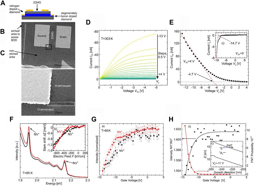
FIGURE 12. (A) Schematic diagram of final equipment. (B) SEM image of the outside of the device. (C) A magnified view of the surface. (D) In a 0.5 V step, the iv characteristic of the grid voltage is applied between Vg = −13 v and+4v. (E) Threshold value voltage Vth = −4.7 V transconductance. (F) shows a photoluminescence spectrum with gate voltages of −14 V (black) and −9 V (red) and laser excitation power of 500 μW [b) shows a significant shift between neutral (black) and negatively charged nv centers (red)]. (G) The normalized intensity of the two charge states in the NV center depends on the gate voltage. (H) NV/NV0 ratio of gate voltage between Vg = −14 v and+4v (black box) [c) Schematic diagram of electron tunneling from 3e state to Fowler-Nordheim tunneling (FNT) of conduction band] [57].
7 Ultraviolet detector
With the development of electronic engineering and optical technology, ultraviolet (UV) detectors are receiving increasing attention, and their applications have boomed in the last decade, including energy, defense, space communications, medical, food processing and water treatment. However, in response to the above practical applications, many studies have focused on achieving efficient and highly stable operation of equipment in harsh environments, thus seeking high-performance materials and functional structures [59]. Diamond-based UV detectors are very promising candidates for use in harsh environments. It has high thermal conductivity, high resistivity, high carrier mobility and a large band gap (5.5eV). The latter makes it insensitive to visible radiation, so diamond also shows great potential in the manufacture of radiation detection equipment [60, 61]. In addition, its low atomic number and ability to withstand high radiation flux allow it to be used as a beam monitor without significantly changing the performance of the interacting beams [62]. Liu et al. [63] fabricated a 3D diamond photodetector with high response speed and low dark current using a bottom-up approach. Their measurements showed that the photovoltaic detectors exhibited typical rectifier I-V characteristics, with a dark current of 14.2 pA at 10 V reverse bias, five orders of magnitude lower than the dark current of the photoconductive detectors. Under the reverse bias of 5V, its rise and decay time are 600 ms and 590 ms, respectively, and no obvious continuous photoconduction phenomenon is shown that the detector was also very responsive. In addition, they also found that the noise equivalent power of the photodetector and the UV/visible light suppression ratio of 215 nm/400 nm are both larger than those of the photoconductance detector. It is concluded that these results may be due to the formation of Schottky barriers and depletion regions between wolfram and oxygenated diamond, which block receptor injection and inhibit the defect light response.
Girolami et al. [64] built and tested a simple vertical MSM UV-C radiation detector. They demonstrated zero deviation operation and detector performance, and found that its performance was comparable to state-of-the-art self-powered, sun-blind UV-C detectors based on wide-gap semiconductors, but with simpler technology. In addition, excellent performance can be obtained even at very weak UV-C irradiated power density (3.7 mW/cm2). When an external bias voltage is applied, the performance of the detector improves significantly, especially in terms of responsiveness. The discovery of inner gain of optical conductivity at high bias voltage is of great significance to the development of diamond detectors. Feng et al. [65] prepared a high-performance metal-semiconduct-metal diamond deep ultraviolet detector with an effective area of 3.093 mm2 by embedding diamond sheets in a polytetrafluoroethylene substrate. Compared with the maximum value of the interfingered intrinsic diamond deep ultraviolet detector, the effective area is increased by more than 6 times, and the photocurrent is increased by about 2 orders of magnitude on the order of milliamperes. Meanwhile, under 3.125 μW mm−2 213 nm illumination and 120 V bias, the response and EQE reach 275.9 A W−1 and 1,607, respectively. This apparent gain is due to a reduction in the height of the Schottky barrier, which is created by the surface state of the light-trapping hole at the metal/diamond interface.
Liu et al. [66] prepared a diamond ultraviolet detector with back contact interfinger electrode structure. The back contact and half fork finger electrodes are connected by a switch, thus allowing the use of both the back contact diamond detector (IBD) and the traditional flat fork finger detector (TID) configuration types in one device. At 150 V bias, switch activation causes increases in light current at 377%, 774%, 464%, 108% and 17% of 240, 235, 230, 225 and 220 nm UV light, respectively shows the fast switching response of a photocurrent with good properties to ultraviolet light. Moreover, IBD has higher response rate and detection rate than TID. Their electric field simulations show that the back electrode can effectively improve the intensity of the field generated in the diamond region. This is because the carrier collection is faster, which improves the detector’s performance, especially at certain wavelengths of ultraviolet light (UV), which has a longer attenuation length in diamond. Sensitivity can be further improved by using high quality diamonds with longer Schubweg. The IBD structure has broad application prospect in ultraviolet detector. Mohapatra et al. [67] studied three different varieties of single crystal diamond photodetectors with different nitrogen concentrations. The measurement diagram is shown in Figure 13A. The UV response current-voltage characteristics of the photodetector are shown in Figure 13B. It is clearly observed that the s1 (single crystal sample of 2 mm × 2 mm) photodetector shows a high UV response current magnitude. They also performed TR-PL measurements (Figure 13C). TR-PL research will link rapid decay with non-radiation recombination to coordinate SRH statistics. The non-radiative lifetime of the color center has been mapped by the ultraviolet response of the photodetector. According to Shockley Read Hall (SRH), photodetectors show a non-radiative lifetime. Combined with the above experiments (UV response, TR-PL measurement), the optical response of the detector is related to the concentration of NV and H3 color centers. In addition, the TR-PL lifetime indicates the prepondering presence of NV centers relative to H3 centers in the diamond sample.
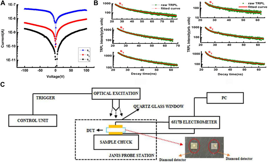
FIGURE 13. (A) Schematic diagram of UV response current measurement. The red arrow indicates a photo of a few DUTs (device under test) with deposited contacts. (B) Three response currents. (C) shows the TRPL lifetimes of the three materials at H3 and NV centers [67].
Liu et al. [68] prepared a kind of ultraviolet detector with p-i-n junction and studied its photoelectric attribute. The detector showed clear rectifying characteristics, with a rectifying ratio of 223 at ±5 V. By measuring the I-V characteristics under different conditions (dark and light) and the spectral response of the detector under different bias voltages, they obtained that the response rate calculated under the reverse bias of 5 V was 1.69 A/W, and the inhibition ratio between 210 nm ultraviolet light and 400 nm visible light is 2.17 × 10³. The time-response characteristics show secular rise times and decay times, which are mainly caused by carrier capture in N-type diamond layers. Therefore, the performance improvement can be achieved by optimizing the device parameters. Chang et al. [69] achieved enhanced ultraviolet absorption by LSPR by assembling palladium nanoparticles on homogeneous epitaxial diamond films. They prepared and studied two kinds of diamond UV detectors, one containing palladium nanoparticles and one without. The structure diagram of the device is shown in Figure 14A. The measured results show (Figure 14B) that the photodetector with palladium nanoparticles has an optical response of 57.28 mA/W at 210 nm light at 5 V, which is 3 orders of magnitude higher than the detector without nanoparticles, and the UV/visible light suppression ratio also reaches 4 orders of magnitude. This first-class performance is attributed to LSPR in palladium nanoparticles. The results of FDTD simulation are highly consistent with this view (Figure 14C). The time transient response measurement results show that the Pd diamond photodetector has good repeatability.
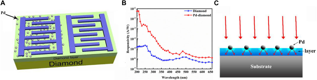
FIGURE 14. (A) with or without Pd nanoparticles diamond photoelectric detector structure diagram. (B) The responsivity of diamond photodetectors with and without pd at 5 V respectively. (C) Effect diagram [69].
8 Diamond photonics or nonlinear optical applications
The most attractive technical basis for on-chip photonic applications is diamond nonlinear optics. Due to the characteristic properties of diamond, such as, wide band gap, high refractive index, large Kerr nonlinearity and very little multi-photon loss, many potonic devices with new functions have appeared. For example, as a quantum communication platform, it integrates a high-Q optical resonator operating at a new wavelength for the generation of frequency combs, compared with existing chip-based nonlinear photonic devices. Therefore, it is not only applied to quantum relations, but is becoming a universal material for various kinds of optical devices. Melchert et al. [70] investigated the performance of on-chip diamond waveguides in controlling light generation. Their theoretical basis is nonlinear soliton dynamics. Various transport dynamics can be achieved through diamond photonics, including supercontinuum generated by soliton fission. Compared to conventional silica based optical fibers (where this process occurs in meters), diamond only requires a propagation distance of millimeters to be sufficient. They realized that the transport dynamics of solitons before fission are always characterized by pulse narrowing, and realized pulse compression using a diamond platform, which provides the possibility to break the compression factor record.
Dory et al. [71] employed an chottkyion-based reverse design approach to overcome the limitations of cutting-edge diamond nanomanufacturing and develop efficient blocks for diamond nanophotonics. In small diamond photonic circuits and optical free-space couplers, they achieved key characteristics of high efficiency, compact-ness and robustness. Their research can be well applied to complex quantum circuits, where compact solutions for various device components such as optical separators, phase retarders and mode converters are critical. Moreover, diamond nitrogen vacancy (NV) centers have broad application prospects in quantum computing and sensing applications. Using optical waveguides to connect multiple diamond NV together is an important research direction in diamond photonics. Sotillo et al. [72] demonstrated that femtosecond laser micromachining can use type II (optical mode constraint between two closely parallel laser engraving modification lines) geometric shapes to etch buried and single-mode optical waveguides in diamond. It is also possible to form a single NV center in the diamond body using ordinary beam forming methods. The cornerstone of the diamond photonics platform is an optical circuit written with a laser and an NV center, which enables quantum information systems with optically connected entangled qubits, while enabling photomagnetometers with high sensitivity and high resolution.
Wan et al. [73] integrated diamond waveguide arrays into an aluminum nitride photonic platform, offering hope for scalable chips that enable quantum information processing. They demonstrated a massive diamond photonic chip with 128 bits, all of which have nearly the same spin quanta. Their ingenuity lies in establishing a combined system that combines diamond waveguides as the host of color centers with aluminum nitride (AlN) platforms as photonic integrated circuits (PICs) and “photonic buses”. AlN’s wide transparent window, which can be used in large wafers, and established nanofabrication protocols make it possible to design the required photonic chips.
Motojima et al. [75] used 40 fs femtosecond laser pulses to investigate the effect of nitrogen vacancy (NV) centers in diamond on nonlinear optical effects, specifically the OKE and TPA at 800 nm light. When the NV center is introduced, both nonlinear optical effects are enhanced. Importantly, the signal enhancement of time-resolved reflectance measurements is more pronounced than that of traditional transmission measurements. Their findings will open new windows for the development of all optical quantum sensing and computation based on nonlinear optical effects, such as single-photon sources using waveguides or nanocolumn structures, all of this helps to enable quantum technology with a wide range of frequency resolutions and spaces.
9 Conclusions and future perspective
New applications of diamond-related structures in optoelectronic devices such as ultraviolet detectors, transistors, sensors, LEDs, and memory have received much attention in the past 10 years. Although devices based on diamond structures show good performance in a variety of optoelectronic applications, researchers are still looking for new manufacturing techniques to improve the optical and electrical properties of these devices. For example, injecting dopants into diamond film structures or allowing them to be integrated with different substrates can make the synthesized new structures have better electrical conductivity, heat dissipation, compressive resistance and higher response rate, which may have important implications for future optoelectronic applications. In addition, a better development of devices with diamond structures requires an understanding of the physical transport mechanism of the devices, so rigorous data fitting using relevant semiconductor theories and computational models is essential.
As a kind of multi-purpose material, diamond structure still has a long way to go in refining its preparation process and performance, and exploring diamond composite materials with stable structure and steerable performance will become a major trend in the future. It is very important to study different diamond structures and different building-up process for enhancing the application of diamond structures in photoelectric devices. For example, the current unsatisfactory diamond detector is mainly due to signal problems caused by impurities and defects of polycrystalline materials. The breakthrough to figure out the puzzle is to improve the quality of synthetic diamond. The detector signal prepared by synthetic diamond is smaller than that of natural diamond, and the spatial uniformity of response also needs to be improved. Further efforts are needed to study diamond-related photoelectric devices in new areas such as detection and communication. P-type boron doped diamond can enhance its electrical resistivity, diamond can be transformed from an insulator into a semiconductor or even a superconductor and can be used in combination with various n-type semiconductor such as WO3, TiO2, MoS2 and GaN to form PN heterojunctions. Therefore, it is possible to improve the performance of optoelectronic devices, including UV detectors, transistors, sensors and LEDs, by attempting to manufacture diamond heterojunction devices for high temperature, high power and radiation-proof environment.
Author contributions
Conceptualization, DS and HF; methodology, LZ and HF; investigation, YY, HF, and LZ; formal analysis, YY, CW, and SG; writing—original draft, QW and YY; data curation, DS, JF, and QW; writing—review and editing, DS, JF, and QW; supervision, DS and CW; software, LZ and SG; visualization, LZ; validation, DS and JF; resources,; funding acquisition, DS and QW. All authors contributed to the article and approved the submitted version.
Funding
This research was funded by the following: the National Natural Science Foundation of China (Grant Nos. 62104090 and 11604133), the Natural Science Foundation of Shandong Province (Grant No. ZR2017QA013), the Science and Technology Plan of Youth Innovation Team for Universities of Shandong Province (Grant No. 2019KJJ019), the Introduction and Cultivation Plan of Youth Innovation Talents for Universities of Shandong Province, the Special Construction Project Fund for Shandong Province Taishan Scholars, the Open Project of State Key Laboratory of Superhard Materials (Jilin University, Grant Nos. 201503 and 201612), the Fundamental Research Funds for the Central Universities (buctrc 202122), the Research Funding of Liaocheng University (Grant Nos. 318012016, 318051610, and 318051612).
Conflict of interest
DS, JF, and QW were employed by Shandong Liaocheng Laixin Powder Materials Science and Technology Co., Ltd.
The remaining authors declare that the research was conducted in the absence of any commercial or financial relationships that could be construed as a potential conflict of interest.
Publisher’s note
All claims expressed in this article are solely those of the authors and do not necessarily represent those of their affiliated organizations, or those of the publisher, the editors and the reviewers. Any product that may be evaluated in this article, or claim that may be made by its manufacturer, is not guaranteed or endorsed by the publisher.
References
1. Lee YT, Vardi A, Tordjman M. A hybrid self-aligned MIS-MESFET architecture for improved diamond-based transistors. Appl Phys Lett (2020) 117:202101. doi:10.1063/5.0023662
2. Noh J, Alajlouni S, Tadjer MJ, Culbertson JC, Bae H, Si MW, et al. High performance β-Ga2O3 nano-membrane field effect transistors on a high thermal conductivity diamond substrate. IEEE J Electron Devices Soc (2019) 7:914–8. doi:10.1109/JEDS.2019.2933369
3. Grezes C, Kubo Y, Julsgaard B, Umeda T, Isoya J, Sumiya H, et al. Towards a spin-ensemble quantum memory for superconducting qubits. C R Phys (2016) 17:693–704. doi:10.1016/j.crhy.2016.07.006
4. Kosowska M, Majchrowicz D, Sankaran KJ, Ficek M, Haenen K, Szczerska M. Doped nanocrystalline diamond films as reflective layers for fiber-optic sensors of refractive index of liquids. Metals-basel (2019) 12:2124. doi:10.3390/ma12132124
5. Sung JC, Kan MC, Hu SC, Yuan JCC, Sung M. Diamond islands wafer for super LED manufacture. ECS Trans (2010) 27:971–6. doi:10.1149/1.3360738
6. Zhang XY, Ma HL, Zhao YM, Yao N, Zeng FG. Effect of different metal composite layer on field emission properties of diamond film. Adv Mater Res (2021) 586:181–4. doi:10.4028/www.scientific.net/AMR.586.181
7. Liu ZC, Zhao D, Zhu TF, Wang J, Yi WY, Min T, et al. Enhanced responsivity of diamond UV detector based on regrown lens structure. IEEE Electron Device Lett (2020) 41:1829–32. doi:10.1109/LED.2020.3033824
8. Shim EL, Lee MH, Lu MY, Kang CJ, Lee KW, Choi YJ. Superior field emissions from boron-doped nanocrystalline diamond compared to boron-doped microcrystalline diamond. J Nanosci Nanotechnol (2012) 12:8904–7. doi:10.1166/JNN.2012.6702
9. Marathe S, Koinkar P, Ashtaputre S, Sathe V, More MA, Kulkarni SK. Enhanced field emission from ZnO nanoneedles on chemical vapour deposited diamond films. Thin Solid Films (2010) 518:3743–7. doi:10.1016/j.tsf.2009.10.118
10. Torresin O, Borz M, Mauchain J, Blum L, Kleshch VL, Obraztsov AN, et al. Conduction mechanisms and voltage drop during field electron emission from diamond needles. Ultramicroscopy (2019) 202:51–6. doi:10.1016/j.ultramic.2019.03.006
11. Lloret F, Sankaran KJ, Millan-Barba J, Desta D, Rouzbahani R, Pobedinskas P, et al. Improved field electron emission properties of phosphorus and nitrogen co-doped nanocrystalline diamond films. Nanomaterials (2020) 10:1024. doi:10.3390/nano10061024
12. Chubenko O, Baturin SS, Kovi KK, Sumant AV, Baryshev SV. Locally resolved electron emission area and unified view of field emission from ultra nanocrystalline diamond films. ACS Appl Mater Inter (2017) 9:33229–37. doi:10.1021/acsami.7b07062
13. Sankaran JK, Panda K, Hsieh PY, Pobedinskas P, Park JY, Bael MKV, et al. Low temperature synthesis of lithium-doped nanocrystalline diamond films with enhanced field electron emission properties. Nanomaterials (2018) 8:653. doi:10.3390/nano8090653
14. Chen CK, Tang BJ, Xu H, Pan JP, Jiang MY, Li X, et al. Low-defect nanodiamonds and graphene nanoribbons enhanced electron field emission properties in ultra nanocrystalline diamond films. ACS Appl Electron Mater (2021) 3:1648–55. doi:10.1021/acsaelm.0c01111
15. Huang L, Harajiri S, Wang SQ, Wu XQ, Teii K. Enhanced field emission from ultra nanocrystalline diamond-decorated carbon nanowalls prepared by a self-assembly seeding technique. ACS Appl Mater Inter (2022) 14:4389–98. doi:10.1021/acsami.1c17279
16. Ficek M, Dec B, Sankaran KJ, Gajewski K, Tatarczak P, Wlasny L, et al. Stable field electron emission and plasma illumination from boron and nitrogen Co-doped edge-rich diamond-enhanced carbon nanowalls. Adv Mater Inter (2021) 8:2100464. doi:10.1002/admi.202100464
17. Zhang XY, Ma HL, Zhao YM, Yao N, Zeng FG, Zhang BL. Comparative studies on field emission properties of diamond and diamond/Ti films. Adv Mater Res (2012) 586:177–80. doi:10.4028/www.scientific.net/AMR.586.177
18. Li HN, Xiong Y, Wang B, Yang B, Huang N, Liu Y, et al. Microstructural modification of diamond-graphite nanohybrid films via adjusting deposition temperatures for enhanced electron field emission. Diamond Relat Mater (2018) 87:228–32. doi:10.1016/j.diamond.2018.06.003
19. Kolekar SK, Godbole RV, Godbole VP, Dharmadhikari CV. Electron transport across nanocrystalline diamond films: field emission and conducting atomic force microscopic investigations. AIP Adv (2020) 10:045129. doi:10.1063/1.5142565
20. Perez G, Chicot G, Avenas G, Lefranc P, Jeannin PO, Eon D, et al. Integrated temperature sensor with diamond Schottky diodes using a thermosensitive parameter. Diamond Relat Mater (2017) 78:83–7. doi:10.1016/j.diamond.2017.08.008
21. Bachmair F. Diamond sensors for future high energy experiments. Nucl Instrum Methods Phys Res Sect A (2016) 831:370–7. doi:10.1016/j.nima.2016.03.039
22. Possasa M, Rousseaua L, Ghassemia F, Lissorguesa G, Gonzalesa P, Scorsoneb E, et al. Comparing silicon and diamond micro-cantilevers based sensors for detection of added mass and stiffness changes. Proced Eng (2015) 120:1115–9. doi:10.1016/j.proeng.2015.08.807
23. Shen W, Wu G, Li LJ, Li H, Liu S, Shen SN, et al. Fluorine-terminated diamond (110) surfaces for nitrogen-vacancy quantum sensors. Carbon (2022) 193:17–25. doi:10.1016/j.carbon.2022.02.017
24. Bähr M, Jahn M, Heinze C, Neckermann K, Meijer J, Ortlepp T. Compact all-optical quantum sensor device based on nitrogen vacancy centers in diamond. Phys Status Solidi A (2023) 220:2200338. doi:10.1002/pssa.202200338
25. Liua KS, Henningb A, Heindla MW, Allerta RD, Bartla JD, Sharpb ID, et al. Surface NMR using quantum sensors in diamond. Proc Natl Acad Sci U S A (2022) 119:2111607119. doi:10.1073/pnas.2111607119
26. Salvatori S, Pettinato S, Piccardi A, Sedov V, Voronin A, Ralchenko V. Thin diamond film on silicon substrates for pressure sensor fabrication. Materials (2020) 13:3697. doi:10.3390/ma13173697
27. Pettinato S, Barettin D, Sedov V, Ralchenko V, Salvatori S. Fabry-perot pressure sensors based on polycrystalline diamond membranes. Materials (2021) 14:1780. doi:10.3390/ma14071780
28. Zhang QW, Du YX, Chang XH, Xu BQ, Chen GQ, He S, et al. Partly-O-diamond solution-gate field-effect transistor as an efficient biosensor of glucose. J Electrochem Soc (2023) 170:037507. doi:10.1149/1945-7111/aca8d4
29. Guthoff M. The new fast beam condition monitor using poly-crystalline diamond sensors for luminosity measurement at CMS. Nucl Instrum Methods Phy Res (2019) 936:717–8. doi:10.1016/j.nima.2018.11.071
30. Belwanshi V, Topkar A. Quantitative analysis of MEMS piezoresistive pressure sensors based on wide band gap materials. IETE J Res (2022) 68:667–77. doi:10.1080/03772063.2019.1620641
31. Xu ZY, Zhu SQ, Yang WL. Quantum-memory-assisted entropic uncertainty relation with a single nitrogen-vacancy center in diamond. Appl Phys Lett (2012) 101:244105. doi:10.1063/1.4771988
32. Poem E, Weinzetl C, Klatzow J, Kaczmarek KT, Munns JHD, Champion TFM, et al. Broadband noise-free optical quantum memory with neutral nitrogen-vacancy centers in diamond. Phys Rev B (2015) 91:205108. doi:10.1103/PhysRevB.91.205108
33. England DG, Fisher KAG, MacLean JPW, Bustard PG, Lausten R, Resch KJ, et al. Storage and retrieval of THz-bandwidth single photons using a room-temperature diamond quantum memory. Phys Rev Lett (2015) 114:053602. doi:10.1103/PhysRevLett.114.053602
34. Battistoni S, Carcione R, Tamburri E, Erokhin V, Terranova ML, Iannotta S. A Ti-doped chemical vapor deposition diamond device as artificial synapse for neuromorphic applications. Adv Mater Technol (2023) 8:2201555. doi:10.1002/admt.202201555
35. Tuissi A, Biffi CA, Ruella S, Casati R. High performance shape memory effect (HP-SME) for new shape memory devices: a diamond-like actuator. Mater Today Proc (2015) 2:S975–8. doi:10.1016/j.matpr.2015.07.444
36. Grigoreva L, Razdolsky A, Kazachenko V, Strakhova N, Grigorev V. Memory effect in the spatial series based on diamond and graphite crystals. Molecules (2020) 25:5387. doi:10.3390/molecules25225387
37. Cheng Z, Bai TY, Shi JJ, Feng TL, Wang YK, Mecklenburg M, et al. Tunable thermal energy transport across diamond membranes and diamond-Si interfaces by nanoscale graphoepitaxy. ACS Appl Mater Inter (2019) 11:18517–27. doi:10.1021/acsami.9b02234
38. Ke WC, Chiang CY, Kim TG, Lin YC, Liao CY, Chang KJ, et al. Nitrogen doped ultra nanocrystalline diamond conductive layer grown on InGaN-based light-emitting diodes using nanopattern enhanced nucleation. Appl Surf Sci (2021) 546:149052. doi:10.1016/j.apsusc.2021.149052
39. Toole MO, Diamond D. Absorbance based light emitting diode optical sensors and sensing devices. Sensors (2008) 8:2453–79. doi:10.3390/s8042453
40. Kyatam S, Rodrigues L, Maslovski S, Alves LN, Mendes JC. Improving the reliability of power LEDs with diamond boards. Diamond Relat Mater (2022) 127:109144. doi:10.1016/j.diamond.2022.109144
41. Chen PH, Lin CL, Liu YK, Chung TY, Liu CY. Diamond heat spreader layer for high-power thin-GaN light-emitting diodes. IEEE Photonic Tech L (2008) 20:845–7. doi:10.1109/LPT.2008.921826
42. Xie RJ, Li ZQ, Guo SL, Wang ZG, Xue H. High bandwidth GaN-based blue LEDs using Ag-grating and diamond heat sink. Photon Nanostruct (2020) 42:100856. doi:10.1016/j.photonics.2020.100856
43. Geis MW, Wade TC, Wuorio CH, Fedynyshyn TH, Duncan B, Plaut ME, et al. Progress toward diamond power field-effect transistors. Phys Status Solidi A (2018) 215:1800681. doi:10.1002/pssa.201800681
44. Imura M, Hayakawa R, Ohsato H, Watanabe E, Tsuya D, Nagata T, et al. Development of AlN/diamond heterojunction field effect transistors. Diamond Relat Mater (2012) 24:206–9. doi:10.1016/j.diamond.2012.01.020
45. Imura M, Hayakawa R, Watanabe E, Liao MY, Koide Y, Amano H. Demonstration of diamond field effect transistors by AlN/diamond heterostructure. Phys Status Solidi RRL (2011) 5:125–7. doi:10.1002/pssr.201105024
46. Kato H, Oyama K, Makino T, Ogura M, Takeuchi D, Yamasaki S. Diamond bipolar junction transistor device with phosphorus-doped diamond base layer. Diamond Relat Mater (2012) 27–28:19–22. doi:10.1016/j.diamond.2012.05.004
47. Izak T, Krátká M, Kromka A, Rezek B. Osteoblastic cells trigger gate currents on nanocrystalline diamond transistor. Colloids Surf B (2015) 129:95–9. doi:10.1016/j.colsurfb.2015.03.035
48. Dankerl M, Hauf MV, Stutzmann M, Garrido JA. Diamond solution-gated field effect transistors: properties and bioelectronic applications. Phys Status Solidi A (2012) 209:1631–42. doi:10.1002/pssa.201200345
49. Song KS, Zhang GJ, Nakamura YU, Furukawa K, Hiraki T, Yang JH, et al. Label-free DNA sensors using ultrasensitive diamond field-effect transistors in solution. Phys Rev E (2006) 74:041919. doi:10.1103/PhysRevE.74.041919
50. Ruslinda AR, Tajima S, Ishii Y, Ishiyama Y, Edgington R, Kawarada H. Aptamer-based biosensor for sensitive PDGF detection using diamond transistor. Biosens Bioelectron (2010) 26:1599–604. doi:10.1016/j.bios.2010.08.002
51. Zhang MH, Wang W, Chen GQ, Wen F, Lin F, He S, et al. Electrical properties of cerium hexaboride gate hydrogen-terminated diamond field effect transistor with normally-off characteristics. Carbon (2023) 201:71–5. doi:10.1016/j.carbon.2022.08.056
52. Choi U, Kwak T, Han S, Kim SW, Nam O. High breakdown voltage of boron-doped diamond metal semiconductor field effect transistor grown on freestanding heteroepitaxial diamond substrate. Diamond Relat Mater (2022) 121:108782. doi:10.1016/j.diamond.2021.108782
53. Shur M, Rudin S, Rupper G, Ivanov T. p-Diamond as candidate for plasmonic terahertz and far infrared applications. Appl Phys Lett (2018) 113:253502. doi:10.1063/1.5053091
54. Lundh JS, Shoemaker D, Birdwell AG, Weil JD, Cruz LMDL, ShahAppl PB, et al. Thermal performance of diamond field-effect transistors. Phys Lett (2021) 119:143502. doi:10.1063/5.0061948
55. Huang BQ, Bai XW, Lam SK, Tsang KK. Diamond FinFET without hydrogen termination. Sci Rep (2018) 8:3063. doi:10.1038/s41598-018-20803-5
56. Syamsul M, Oi N, Okubo S, Kageura T, Kawarada H. Heteroepitaxial diamond field-effect transistor for high voltage applications. IEEE Electron Device Lett (2018) 39:51–4. doi:10.1109/LED.2017.2774290
57. Oing D, Ney M, Bendt G, Schulz S, Geller M, Wohrl N, et al. A monolithic, back-gated diamond field-effect transistor for tunable color centers. Diamond Relat Mater (2021) 119:108597. doi:10.1016/j.diamond.2021.108597
58. Zhang YH, Shur MS. P-Diamond, Si, GaN, and InGaAs TeraFETs. IEEE Trans Electron Device (2020) 67:4858–65. doi:10.1109/TED.2020.3027530
59. Lin CR, Wei DH, BenDao MK, Chen WE, Liu TY. Development of high-performance UV detector using nanocrystalline diamond thin film. Int J Photoenergy (2014) 2014:1–8. doi:10.1155/2014/492152
60. Caylar B, Pomorski M, Bergonzo P. Laser-processed three dimensional graphitic electrodes for diamond radiation detectors. Appl Phys Lett (2013) 103:043504. doi:10.1063/1.4816328
61. Caiffia B, offeyc IC, Pillonb M, Osipenkod M, Prestopinoe G, Ripanid M, et al. Analysis of the response of CVD diamond detectors for UV and sX-Ray plasma diagnostics installed at JET. Phys Proced (2015) 62:79–83. doi:10.1016/j.phpro.2015.02.014
62. Schirru F, Lohstroh A, Jayawardena KDJI, Henley SJ, Sellin PG. X-ray induced photocurrent characteristics of CVD diamond detectors with different carbon electrodes. J Instrum (2013) 8:C12046. doi:10.1088/1748-0221/8/12/C12046
63. Liu ZC, Zhao D, Min T, Wang J, Chen GQ, Wang HX. Photovoltaic three-dimensional diamond UV photodetector with low dark current and fast response speed fabricated by bottom-up method. IEEE Electron Device Lett (2019) 40:1186–9. doi:10.1109/LED.2019.2919922
64. Girolami M, Serpente V, Mastellone M, Tardocchi M, Rebai M, Xiu QL, et al. Self-powered solar-blind ultrafast UV-C diamond detectors with asymmetric Schottky contacts. Carbon (2022) 189:27–36. doi:10.1016/j.carbon.2021.12.050
65. Feng MY, Jin P, Meng XQ, Xu PF, Huo XD, Zhou GD, et al. Performance of metal-semiconductor-metal structured diamond deep-ultraviolet photodetector with a large active area. J Phys D: Appl Phys (2022) 55:404005. doi:10.1088/1361-6463/ac83ce
66. Liu K, Liu BJ, Zhao JW, Shu GY, Xu XC, Yao KL, et al. Application of back bias to interdigital-electrode structured diamond UV detector showing enhanced responsivity. Sens Actuators, A (2019) 290:222–7. doi:10.1016/j.sna.2019.03.033
67. Mohapatra S, Sahu PK, Rath S, Sahoo PK, Varma S, Narasimha Murty NVL. Impact of nitrogen induced defect dynamics on UV response of diamond photodetectors. Superlattices Microstruct (2020) 142:106504. doi:10.1016/j.spmi.2020.106504
68. Liu ZC, Zhao D, Min T, Wang HX. Fabrication and characterization of (100)-oriented single crystal diamond p-i-n junction ultraviolet detector. Phys Status Solidi A (2020) 217:2000207. doi:10.1002/pssa.202000207
69. Chang XH, Wang YF, Zhang XF, Liu ZC, Fu G, Zhao D, et al. Enhanced ultraviolet absorption in diamond surface via localized surface plasmon resonance in palladium nanoparticles. Appl Surf Sci (2019) 464:455–7. doi:10.1016/j.apsusc.2018.09.087
70. Melchert O, Kinnewig S, Dencker F, Perevoznik D, Willms S, Babushkin L, et al. Soliton compression and supercontinuum spectra in nonlinear diamond photonics. Diam Relat Mater (2023) 136:109939. doi:10.1016/j.diamond.2023.109939
71. Dory C, Vercruysse D, Yang KY, Sapra NV, Rugar AE, Sun S, et al. Inverse-designed diamond photonics. Nat Commun (2019) 10:3309. doi:10.1038/s41467-019-11343-1
72. Sotillo B, Bharadwaj V, Hadden JP, Rampini S, Chiappini A, Fernandez TT, et al. Visible to infrared diamond photonics enabled by focused femtosecond laser pulses. Micromachines (2017) 8:60. doi:10.3390/mi8020060
73. Wan NH, Lu TJ, Chen KC, Walsh MP, Trusheim ME, Santis LD, et al. Large-scale integration of artificial atoms in hybrid photonic circuits. Nature (2020) 583:226–31. doi:10.1038/s41586-020-2441-3
74. Kianinia M, Aharonovich L. Diamond photonics is scaling up. Nat Photon (2020) 14:599–600. doi:10.1038/s41566-020-0695-9
Keywords: diamond, diamond-based, wide bandgap, photoelectric application, harsh condition
Citation: Fei H, Sang D, Zou L, Ge S, Yao Y, Fan J, Wang C and Wang Q (2023) Research progress of optoelectronic devices based on diamond materials. Front. Phys. 11:1226374. doi: 10.3389/fphy.2023.1226374
Received: 23 May 2023; Accepted: 31 July 2023;
Published: 10 August 2023.
Edited by:
Yaping Dan, Shanghai Jiao Tong University, ChinaReviewed by:
Massimo Cazzanelli, University of Trento, ItalyRuozheng Wang, Xi’an Jiaotong University, China
Copyright © 2023 Fei, Sang, Zou, Ge, Yao, Fan, Wang and Wang. This is an open-access article distributed under the terms of the Creative Commons Attribution License (CC BY). The use, distribution or reproduction in other forums is permitted, provided the original author(s) and the copyright owner(s) are credited and that the original publication in this journal is cited, in accordance with accepted academic practice. No use, distribution or reproduction is permitted which does not comply with these terms.
*Correspondence: Dandan Sang, c2FuZ2RhbmRhbkBsY3UuZWR1LmNu; Cong Wang, d2FuZ2NvbmdwaHlzaWNzQG1haWwuYnVjdC5lZHUuY24=; Qinglin Wang, d2FuZ3FpbmdsaW5AbGN1LmVkdS5jbg==
†ORCID ID: Cong Wang, orcid.org/0000-0002-3073-8853