 Nan Li
 Kai Wu
94% of researchers rate our articles as excellent or good
Learn more about the work of our research integrity team to safeguard the quality of each article we publish.
Find out more
ORIGINAL RESEARCH article
Front. Phys., 25 July 2023
Sec. Low-Temperature Plasma Physics
Volume 11 - 2023 | https://doi.org/10.3389/fphy.2023.1223704
This article is part of the Research TopicElectrical Breakdown and Discharge Plasma at Small Scales: Characteristics, Mechanisms, and ApplicationsView all 6 articles
The quantum effects of space charge on electron field emission have been widely investigated since the last century. When electrons energy and their mean spacing approach the Hartree level and the de Broglie wavelength respectively, the influence of the quantum effects on the field emission current becomes significant. In this work, by developing an in-house software, we self-consistently solve the one-dimensional Poisson-Schrödinger equation together with the Wentzel-Kramers-Brillouin-Jeffreys (WKBJ) model for metal-vacuum-metal nanogaps, after considering the anode screening effect, space charge Coulomb potential and exchange-correlation effects simultaneously. Employing the method, the electron field emission characteristics were studied by varying the nanogap spacing (D) and the electric field strength (F), and four different emission regimes including quantum regime (QR), space charge limited regime (SCLR), direct tunnelling regime (DTR) and field emission regime (FER) are defined. The influences of space charge field components on the field emission characteristics and space charge distribution are analyzed for different emission regimes in nanogap. In addition, the impact of using different exchange-correlation functionals (LDA, GGA and meta-GGA) on Jacob’s ladder for describing the quantum effects of space charge on the electron emission current density was analyzed. Finally, electron field emission properties of one-dimensional (1-D) nanogaps consisting of refractory metals (W and Mo) as well as the three-dimensional (3-D) nano-tip are discussed to elucidate the impact of the exchange-correlation effects on the enhanced field emission process at nanoscale.
Filed emission phenomenon commonly occurs in micro- and nano-electronic devices when the local electric field on the surface of the metal electrode is high enough. Many modern technologies crucially rely on the electron field emission process such as electron microscopes (scanning electron microscopy and transmission electron microscopy), X-ray tube, high power microwave sources, surface conduction electron emitter displayer, and MEMS systems [1–8]. Moreover, the electrode spacing in field emission devices nowadays can even reach the nanometer in nanogap resistance switches and nanogap scanning probe microscopes [9, 10].
The underlying physics of field emission phenomenon has been extensively studied since the beginning of the 20th century, leading to the famous Fowler-Nordheim (FN) law which is widely used to calculate the emission current density for electron field emission devices [11–15]. Nevertheless, the validity of F-N law is very often questioned for small gap with large emission current density [16]. In the latter case, the classical Child-Langmuir (CL) law should be used to calculate the space-charge-limited current density [17]. However, both FN law and CL law could fail to accurately calculate the field emission characteristics in a nanogap. Additional mechanisms must be considered for predicting field emission properties of nanogap, including the image charge potentials between space charges and electrodes (cathode and anode), and space charge potentials such as Coulomb potential and exchange-correlation potential. Those physical effects could directly influence the electron emission barrier heights and tunnelling probability in nanogap system [18].
As for the study of electron field emission in a nanogap, few representative works are worth mentioning here. In 1963, Simmons extended the FN law in calculating the field emission characteristics of nano-gap by including the anode screening effect in terms of image charge potential [19]. Simmons model could explain the electron direct tunnelling phenomenon in nano-gap system, but the image charge potential in the model is approximated by the classic Coulomb potential. In addition, Simmons model does not consider the space charge potentials, i. e., the Coulomb interaction and exchange-correlation effects among emitted electrons. Later on, Y. Y. Lau studied the space charge effects on electron field emission in nanogaps, and also derived the famous quantum CL law for large current regime of nanogaps in 1990 [20]. Furthermore, after including the exchange-correlation effects of space charges, L. K. Ang found a new scaling relationship for emission current density versus V1/2 and D−4 in the quantum CL law [21]. More recently, W. S. Koh and L. K. Ang proposed a one-dimensional quantum field emission model which includes the space charge Coulomb potential, exchange-correlation effects, and image charge potentials between space charges and electrodes [22]. To eliminate the singularities in the image charge potential at the boundaries between electrodes and vacuum due to the use the classic Coulomb potential form in the FN law and Simmons model, the modified Thomas–Fermi free electron model is employed for computing image charge potential [18].
Previous studies have demonstrated the transitions from the classical field emission regime to the quantum regime, or from the classic FN law (low current density) to the space charge limited CL law (large current) in a nanogap. However, significance of the exchange-correlation effects has not been thoroughly studied in the quantum electron field emission regime. The transitions between different electron field emission regimes and their corresponding boundaries are not well understood in nanogaps. On the other hand, local density approximation (LDA) has been employed to treat the exchange-correlation effects among space charges, which may not properly describe the non-uniformity of space charge density distribution in nanogaps. Other semilocal exchange-correlation density functionals such as generalized gradient approximation (GGA) and meta-generalized gradient approximation (meta-GGA) are expected to provide more reliable description for the quantum effects of non-uniform space charges in nanogaps [23–25].
In this work, we developed an in-house code for calculating the electron field emission density with the inclusion of space charge quantum many-body effects under the Wentzel-Kramers-Brillouin-Jeffreys (WKBJ) framework. The one-dimensional modified Poisson-Schrödinger equation combined with WKBJ electron field emission model is solved numerically to understand the field emission characteristics in metal-vacuum-metal nanogaps. In the modified model, the space charge Coulomb potential, exchange-correlation potential and image charge potential are all included using the appropriate forms. Furthermore, the exchange-correlation effects of space charges are not only numerically considered using local density approximation (LDA), but also other higher level semilocal density functionals on Jacob’s ladder of density functional theory (DFT) such as GGA and meta-GGA forms. Based on the current self-consistent numerical results, four distinct electron field emission regimes are recognized based on a better understanding of the dominant physical effect in electron emission by varying the electrode spacing (D) and external E-field strength (F). Besides, we also address the influence of different exchange-correlation functional forms on the electron emission characteristics especially in the quantum regime. Four different systems including “W-Vacuum-W”, “W-Vacuum-Mo”, “Mo-Vacuum-W” and “Mo-Vacuum-Mo” were also studied. Finally, three-dimensional (3-D) ED-MD-PIC simulations were performed using different exchange-correlation functionals to treat the exchange-correlation effects of space charges for a realistic nano-emitter.
To study the field emission phenomenon in a nanogap, we consider the one-dimensional planar “metal-vacuum-metal” system. The electrodes are applied a DC voltage Vg with a spacing D to produce a steady-state electron emission current density J, which is calculated by
Here we use free electron gas model to obtain N(E), which gives the total number of electrons supplied by electron emitter along the x direction (normal to emission surface) with energy between E and E + dE [26]. We adopt the extended Simpson’s rule with rectangular equidistant grids to solve the integral term, as described in detail in A(3) in the Appendix.
The Wentzel-Kramers-Brillouin (WKBJ) method (Kemble formula) is used to calculate the electron transmission probability Db(E) when an electron penetrates a potential barrier U(x) [27].
In Eq. 4, x is the distance from the emitting surface, x1 and x2 are the two intersection points of U(x) with E. When the incident electrons have energy above the maximum value of the potential barrier, the intersection points diminish. In this case, electrons can directly overcome the potential barrier and emit into the vacuum, giving Db(E) = 1. In Eq. 5, U(x) includes five terms: (i) The work function
Specifically, the image charge potential
Here, the Green function of a longitudinal self-consistent field Dvac (p, x, x’) describes the screened Coulomb interaction between the charges at points x and x’, and p is the wavevector along the x direction (field emission direction). Comparing to the classical image charge potential form, the singularities at the interface between electrodes and vacuum are eliminated.
As for the space charges emitted from cathode and which propagate and accumulate in the nanogap, the planar wave function
Here q indicates the normalized wave amplitude,
Regarding the quantum effects of space charges, we use density functional theory (DFT) [29] to calculate the exchange-correlation potential
Where,
Then,
The whole workflow of the numerical calculation is presented in Figure 1, including four steps.
i) Solving Eqs 1 – 5 with WKBJ method to obtain electron emission current density J in nanogap. Solving Eq. 6 to find image charge potential
ii) Substituting the normalized current density
iii) LDA, GGA, and meta-GGA functionals are used to obtain the exchange-correlation potential
iv) Updating the barrier potential U in Eq. 5 with new
FIGURE 1. The workflow of the developed algorithm for self-consistently solving Poisson-Schrödinger equation and WKBJ model to calculate electron emission current density in nanogap.
In order to determine the quantum regime, we calculate the normalized electron emission current density μ = J/JCL, β = J/JFN, where JCL and JFN are the electron emission current densities using CL law and FN law (Murphy and Good formula) [30], respectively. The classic FN law is given by Eq. 12.
Here,
The methodology addressed before was realized in an in-house code, and all related numerical algorithms were implemented using the C++ programing language. Our in-house code can be compiled with the standard C++ compiler on most Linux operating systems. The extension of the 1D-model for nanogaps consisting of planar metal electrodes to the full three-dimensional (3-D) nanogap between the planar and needle-like electrodes was realized using the more advanced hybrid multi-physics and multi-scale modelling method, as available in the FEcMD code [31]. In the hybrid simulation algorithm, the multi-scale self-adaptive finite element meshes were generated and updated dynamically with the atomic structure evolution of metal nano-tip which is treated as the cathode in the typical field emission setup. Such methodology has been routinely employed before to understand the correlation between the electron field emission process and the thermal runaway mechanism of metal nano-tips [32–34]. For 3-D field emission model, the electric field and the emission current density were obtained locally from a quasi-planar like emitter.
Here, we apply the in-house code to calculate the electron field emission characteristics of the benchmark Ba-vacuum-Ba nanogap with a spacing 1 nm to confirm the validity of the methodology and its numerical implementations. The field emission current density versus the applied electric field (F) in a range from 1 V/nm to 100 V/nm for Ba-vacuum-Ba system has been reported before in Ref. [18] by solving Eqs 7, 8. Using the same parameters and PW-LDA functional to those of Ref. [18], the normalized emission current density versus F is shown in Figure 2 for Ba-vacuum-Ba nanogap. For comparison, the same profile obtained in Ref. [18] is also illustrated in Figure 2. The profile obtained from our in-house code is in good agreement with Ref. [18] in a wide range of the applied F value, confirming the validity of our numerical algorithms.

FIGURE 2. The normalized electron emission current density μ = J/JCL as a function of Vg = 1–100 V/nm at D = 1 nm using PW-LDA exchange-correlation functionals for “Ba-Vacuum-Ba” system using our in-house code, compared to that of Ref. [18].
We consider “Ba-Vacuum-Ba” nanogap, where the Fermi Energy (EF) and work function ΦWF of barium (Ba) are given as 2.317 eV and 2.48 eV [35], respectively. The temperature T is set to room temperature 300 K. The exchange and correlation potentials are obtained by employing the LDA in terms of “Slater exchange” and “Perdew and Wang” [23] (fit to the RPA energy) correlation functionals, respectively.
To study the quantum effect on the I-V characteristics of electron emission, the normalized electron emission current density μ = J/JCL is obtained by applying an electric field F from 1 to 100 V/nm with a gap spacing D from 1 nm to 10 nm. For comparison, the classic electron emission current Jclasscial is calculated by setting
In Figure 3A, it is shown that when the applied electric field is large enough (F > 10 V/nm), the normalized electron emission current density is close to the classic CL law (
FIGURE 3. The two-dimensional (2-D) contour plots show the normalized electron emission current density μ = J/JCL as a function of gap spacing (D = 1–10 nm) and E-field strength (F = 1–100 V/nm) for (A) the classical model and (B) the quantum model.
To determine the enclosed boundary of the quantum electron field emission regime where the exchange-correlation effects of space charge play important role in determining the electron transmission energy barrier profile, we calculate the ratio of α = J/Jclassical by varying both F and D, and the results are shown in Figure 4A. It can be seen that the ratio is significantly large (α > 5) in the quantum regime (QR) when the electric field F is about between 2 V/nm and 10 V/nm, and which decreases gradually as the increase of gap spacing. For the very large gap spacing, the field emission current approaches to that of the classic Fowler-Nordheim law.

FIGURE 4. The 2D contour plots show (A) the ratio of electron emission current density of the quantum model to that of the classical model α = J/Jclassical as a function of D = 1–10 nm and F = 1–100 V/nm. The black dash line presents α = 5. (B) The color represents the difference of mean absolute exchange correlation potential minus mean absolute space charge potential
It is known that space charge effect suppresses the electron emission, because the Coulomb repulsion of space charge in the gap can increase electron tunnelling energy barrier height [36]. On the contrary, the exchange-correlation potential of space charges decreases the electron tunnelling potential, enhancing the electron emission. Therefore, we calculate the difference of the mean absolute exchange-correlation potential minus the mean absolute space charge potential
When the applied electric field is relatively small (F < 2 V/nm) in a nanogap, the electron current density is very low so that the influence of space charge potentials (Coulomb and exchange-correlation potentials) is greatly weakened. Figure 5A presents the normalized electron emission current density β = J/JFN when D = 1–10 nm and F = 1–100 V/nm. It shows that the electron current density is close to FN law (β → 1) in field emission regime (FER), while the current surges (β > 100) in direct tunnelling regime (DTR). The normalized mean electron emission energy is shown in Figure 5B, and which is obtained from
FIGURE 5. Normalized field emission parameters as functions of D and F: (A) The normalized electron emission current density β = J/JFN and (B) the normalized average emission electron energy <E>/e Vg as a function of D = 1–10 nm and F = 1–100 V/nm for the quantum model. The black dash line on the bottom left side presents β = 100, and that on the bottom right side presents β = 1 in (A). The Fermi energy EF = 0 in (B).
Figure 6 illustrates four different electron field emission regimes including the QR, SCLR, DTR and FER when D = 1–10 nm and F = 1–100 V/nm in our numerical calculations after considering space charge potentials (image charge, Hartree and exchange-correlation potentials). Otherwise, the different space charge potential components are illustrated in Figure 7 for different electron field emission regimes in nanogaps. Furthermore, the obtained electron wave amplitudes are displayed in Figure 8 for different regimes, showing the effects of space charge potentials on the electron emission intensity in nanogap.
FIGURE 6. Four different electron emission regimes QR (quantum regime), SCLR (space charge limited regime), DTR (direct tunnelling regime), FER (field emission regime) are divided when D = 1–10 nm and F = 1–100 V/nm for the quantum model.
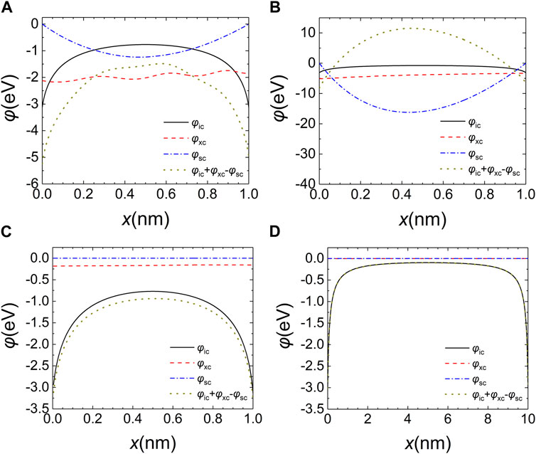
FIGURE 7. The calculated potential profiles in the nanogap for various components in different electron field emission regimes: (A): QR (D = 1 nm and F = 5 V/nm); (B): DTR (D = 1 nm and F = 1 V/nm); (C): SCLR (D = 1 nm and F = 100 V/nm); (D): FER (D = 10 nm and F = 1 V/nm). In all plots, φic denotes the image charge potential, φxc refers to the exchange-correlation potential, and φsc represents the space charge Hartree potential. Obviously, φic + φxc + φsc means the summation of all three potentials. Note that space charge Hartree potential is always positive, and its minus value is shown in all graphs here.
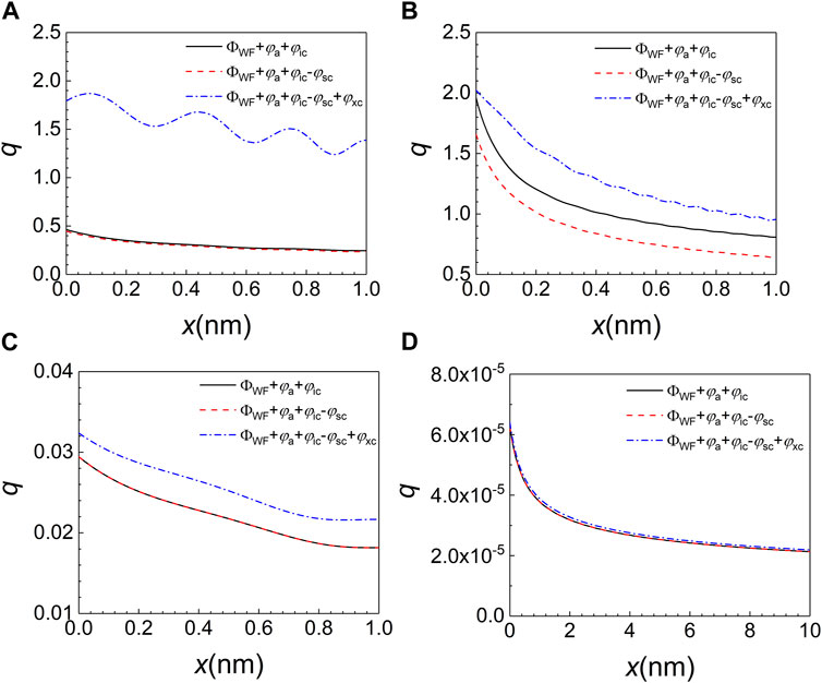
FIGURE 8. The calculated electron wave amplitudes in the nanogap after turning on various space charge potential components in different electron field emission regimes: (A): QR (D = 1 nm and F = 5 V/nm); (B): SCLR (D = 1 nm and F = 100 V/nm); (C): DTR (D = 1 nm and F = 1 V/nm); (D): FER (D = 10 nm and F = 1 V/nm). In all plots, ФWF is the work function of electrode, and φa refers to the applied electronic potential. For other terms, one may refer to Figure 7.
Specifically, the electron emission in the quantum regime (QR) is characterized by a small gap spacing and electric field values in a specified range (2 V/nm < F < 20 V/nm). In this regime, exchange-correlation potential of space charges determines the electron tunnelling energy barrier profile in nanogap. Quantitatively, as shown in Figure 7A, the exchange-correlation potential (φxc) is significantly more negative than that of image charge potential (φic) in the nanogap except for the proximity of electrodes. The space charge Hartree potential (φsc) represents the Coulomb repulsion among emitted electrons in the nanogap, and which is a positive number. Therefore, the exchange-correlation potential plays the role to reduce the energy barrier height in WKBJ model, enhancing the electron emission in QR. Otherwise, the variation of φxc profile in QR is not as strong as that of either φic or φsc. Furthermore, the φxc profile gets less negative when going from left side to right side in nanogap, because the charge density must decrease from the cathode to anode due to the charge continuity condition, i.e., few emitted electrons are found on the right-hand side in nanogap when they are accelerated to a much higher velocity than electrons on the left before reaching the anode. As can be seen from Figure 8A, the obtained electron wave amplitude indeed declines continuously from the cathode to anode in the nanogap. From the same figure, we also clearly see that the inclusion of space charge exchange-correlation potential can greatly boost the field emission current density, compared to all other numerical solutions without such quantum many-body effects. The observed oscillation of q(x) profile in Figure 8A is obviously attributed to the use of a roughly linear triangular potential well (F) in the nanogap for solving the time-independent Schrödinger equation for space charges based on the semi-classical WKBJ model. The oscillating Airy functions are the expected analytical solution for such a potential well. Interestingly, the exchange-correlation potential profile also shows the similar oscillations in Figure 7A, implying that the space charge density determines its magnitude. In conclusion, the field emission property in QR is characterized by the prominent exchange-correlation effects of space charges in the nanogap. However, the overall shape of space charge potentials resembles that of image charge potential.
The space charge limited regime (SCLR) is characterized by the relatively large applied electric field (F > 20 V/nm), as shown in Figure 6. In the SCLR, the electron emission current density is high due to the very large applied electric field value, resulting in the high space charge density in nanogap. As can be seen from Figure 7B, both φic and φxc are negative inside the nanogap. Meanwhile, the φsc gives a very large positive contribution to the overall potential profile (φic + φxc - φsc). The magnitude of the net potential profile is largely determined by φsc in the nanogap for SCLR. Nevertheless, the high space charge density indicate that space charge fields (Hartree and exchange-correlation potentials) are also strong, but Hartree potential plays the dominant role in determining the overall electron tunnelling energy barrier profile. The calculated electron wave amplitudes (q(x)) are depicted in Figure 8B for SCLR with and without the inclusion of space charge potentials. We observe a significant decreasing of q(x) in the nanogap by including the φsc in the field emission model, compared to that of standard WKBJ result (ФWF + φa + φic) with no space charge fields. Further considering the exchange-correlation effects in the calculation enhances the electron wave amplitude, indicating the role of exchange-correlation potential in SCLR is similar to that of QR. Notably, q(x) profile does not oscillate strongly in this case as compared to that of Figure 8A in QR. Due to the very large applied electric field value and small electrode spacing, the energies of space charges approach to that of classic limit where Airy functions exhibit very large quantum numbers. Finally, in Figure 6, we clearly see the transition from the QR to the SCLR by increasing the electric field value. Traditionally, the CL law can be used to evaluate the electron emission current in SCLR.
The direct tunnelling regime (DTR) occurs at the very small gap spacing (D < 2 nm) and the small applied electric field (F < 2 V/nm), as can be seen from Figure 6. In this case, the electron emission current is extremely low, indicating that the space charge potentials (φxc + φsc) are negligible, compared to that of image charge potential. From Figure 7C, it is concluded that the image charge potential determines the electron tunnelling energy barrier. Due to the very small gap spacing, the image charge potential narrows significantly so that electrons below the Fermi level can direct tunnel though the potential barrier into the vacuum. The image charge potential represents the long-range exchange-correlation effects between space charges in the vacuum and electrons that are remain confined in the electrodes (anodes and cathodes in nanogap) [37]. Thus, its origin resembles that of space charge exchange-correlation potential. The image charge potential (φic) can effectively lower the electron tunnelling barrier at the interface between the cathode and vacuum, probably enhancing the electron emission current density in nanogap. The effects of φxc and φsc on the obtained space charge density are plotted in Figure 8C. In the case of DTR, the space charge Hartree potential plays a negligible role in determining the space charge density distribution. Otherwise, the obtained space charge wave amplitude is slightly increased after including the exchange-correlation effects in our self-consistent numerical calculation.
Finally, field emission regime (FER) shows up at large gap spacing (D > 2 nm) with a relatively small applied electric field (F < 2 V/nm) (See Figure 6). As shown in Figure 7D, the exchange-correlation effects (φxc) and the space charge Hartree potential (φsc) can be ignored, because the emission electron density is relatively small in the nanogap with a relatively large gap spacing. The overall space charge field profile is mainly attributed to the image charge potential (φic). Therefore, the electron tunnelling energy barrier profile is obtained from work function (ФWF), applied electrostatic potential (φa) and the image charge potential (φic). As a result, the including of either φxc or φsc almost has no effects on the calculated space charge wave amplitude in the nanogap for FER, as shown in Figure 8D. The electron emission current density in FER is expected to approach that of classic FN law.
In this section, we further investigate the effects of using different exchange-correlation density functionals on the calculated electron emission characteristics. Three widely used local and semilocal density functionals on the first-three rung of Jacob’s ladder are employed in our numerical calculations including the local density approximation (Slater exchange and Perdew-Wang correlation or Perdew-Zunger correlation) [23, 38, 39], Perdew–Burke–Ernzerhof (PBE) [40], strongly constrained and appropriately normed (SCAN) [41]. The normalized electron emission current density μ = J/JCL is obtained for Vg = 1–100 V at D = 1 nm using different exchange-correlation functionals, and the results are plotted in Figure 9A. Besides the emission current density profile obtained from PW-LDA functional, PZ-LDA, PBE and SCAN exchange-correlation functionals predict the very similar normalized emission current density profiles for nanogap (1 nm) by varying the applied electric field value (F). Notably, the lower emission current density is found for PZ-LDA, PBE and SCAN functionals than that of PW-LDA method especially in the quantum regime (QR), as shown in Figure 9A. As a result, the QR is prominent in a wide range for gap spacing using PW-LDA method. The QR shifts to relatively larger gap spacing when using PZ-LDA, PBE and SCAN functionals. Nevertheless, the inclusion of exchange-correlation potential of space charges in the current electron emission model significantly boosts the emission current density in the QR, compared to that of the classic model without considering the quantum many-body effects. Otherwise, all considered exchange-correlation functionals predict that the normalized emission current density approach to that of the quantum CL law (QCL) at large F. Meanwhile, without including the exchange-correlation effects of space charges, the obtained emission current density eventually coincides with the classic CL law. In Figure 9B, the exchange, correlation, and exchange-correlation potential profiles of PW-LDA, PZ-LDA, PBE and SCAN functionals are displayed for D = 1 nm and F = 10 V/nm. The correlation potential of PW-LDA function is more negative than that of PZ-LDA, PBE and SCAN functionals. Meanwhile, the exchange potential profiles of the four functionals do not differ significantly. As a result, the lower electron emission barrier and a higher emission current density are obtained using PW-LDA in the quantum regime. The calculated potential profiles are relatively smooth in nano-gap for PW-LDA, PZ-LDA and PBE methods, compared to those of SCAN functional. Nevertheless, small oscillations are also observed in all exchange or correlation potential profiles obtained from PW-LDA, PZ-LDA and PBE solutions. For those three semilocal density functionals, the oscillations in the exchange or correlation potential profiles reflect the fact that the space charge density distribution shows similar oscillating behavior when solving the Schrödinger equation for the linear triangular potential well in the nanogap. In the case of SCAN, strong counteractive oscillations are seen in the exchange (φx) and correlation (φc) potential profiles across the nanogap. As a result, the exchange-correlation potential (φxc = φx + φc) profile of SCAN functional is remarkably like that of either PZ-LDA or PBE. Therefore, the predicted electron emission current density profiles by PZ-LDA, PBE and SCAN are almost identical. It is also interesting to note that oscillations observed in exchange and correlation potential profiles are indeed more prominent in PBE and SCAN functionals, compared to the potential profiles of LDA. The main difference between LDA and PBE or SCAN functionals is that the former method only needs the electron density profile in nano-gap to calculate the exchange-correlation potential (φxc) and their components (φx and φc). On the other hand, the electron gradient (
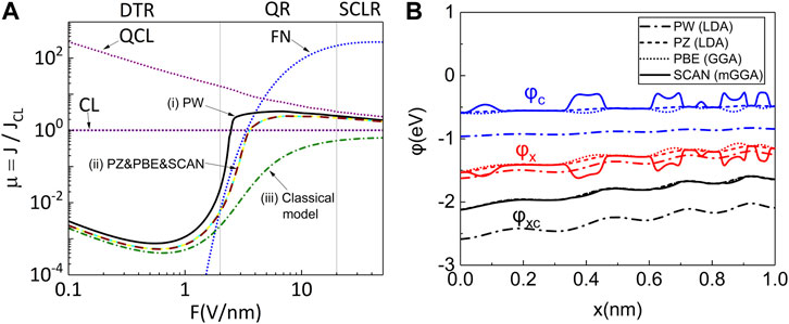
FIGURE 9. The calculated emission current density and potential profiles using different exchange-correlation functionals: (A) The normalized electron emission current density μ = J/JCL as a function of Vg = 1–100 V/nm at D = 1 nm by employing (i) “Perdew and Wang” (fit to the RPA energy) (solid line) (ii) “Perdew and Zunger” (PZ), “Perdew, Burke and Ernzerhof” (PBE) and ‘Sun, Ruzsinszky, and Perdew’ (SCAN) functionals (dashed lines) for the quantum field emission model, respectively. The dotted-dashed line is for (iii) the classical model. The dotted lines represent the well-known Fowler-Nordheim (FN) law without space charge effect, the Child-Langmuir (CL) law and the quantum Child-Langmuir (QCL) law. (B) The exchange-correlation potential φxc, the exchange potential φx and the correlation potential φc of PZ (dashed line), PBE (dotted line) and SCAN (solid line) functionals when D = 1 nm and F = 10 V/nm.
Finally, it is also worth noting that all semilocal functionals employed in this work for calculating the quantum effects of space charges only require the electron density and its gradients as the inputs, the wavefunctions or orbitals of space charges are not evaluated. It is known that most semilocal functionals exhibit self-interaction errors in treating the quantum many-body effects by means of exchange-correlation effects. Whether the presence of self-interaction errors in the employed density functionals significantly affecting the space charge density distribution as well as the electron tunnelling barrier profile in the nanogap for the electron emission process require the development of the methodology that goes beyond the current theoretical framework mainly based on density functional theory. The electron self-interaction errors in both exchange and correlation effects are partly corrected in the construction of SCAN functional [36]. Nevertheless, the overall exchange-correlation potential of SCAN is in close agreement with those of PBE and PZ-LDA in numerical calculations. In current methodology, computing the electron transmission probability and tunnelling barrier profile in the nano-gap only relies on the exchange-correlation potential rather than the use of either of the terms separately. Thus, we do not see a great change of space charge density distribution in the nano-gap by employing the semilocal functionals at various rungs except that of PW-LDA. Overall, we may conclude that the stronger electron field emission is anticipated in the nanogap for the exchange-correlation functional that predicts the more negative potential profile in WKBJ theory, leading to a further expansion of the quantum electron emission regime in Figure 5 in general. Treating the space charge density as the uniform electron gas locally remains a valid approximation to calculate the exchange-correlation effects of space charges in nanogap.
Here, we further apply the methodology to investigate the electron field emission characteristics of nanogaps consisting of like and unlike refractory metals such as W and Mo. Specifically, four different nano-gaps including “W-vacuum-W”, “W-vacuum-Mo”, “Mo-vacuum-W”, and “Mo-vacuum-Mo” configurations are studied in the self-consistent numerical calculations. The spacing of all nanogaps is fixed to 1 nm. In all calculations, the Fermi energies of W and Mo are taken as 5.782 eV and 5.873 eV respectively. Meanwhile, the work functions of W and Mo are given by 4.40 and 4.41 eV respectively [44]. The normalized field emission current density versus the applied E-field value is illustrated in Figure 10. Frist of all, it is noticed that the obtained emission current densities for the four metal-vacuum-metal configurations are almost indistinguishable from each other. However, in the magnified inset, the “W-vacuum-W” and “W-vacuum-Mo” configurations give higher emission current densities than those of “Mo-vacuum-W” and “Mo-vacuum-Mo” cases. It is straightforward to see that W has a slightly lower work function and Fermi energy than those of Mo. Therefore, the cathode determines the field emission current density in the nanogap for QR (quantum emission regime). Secondly, the electron emission current density can be higher than that of classic Child-Langmuir law for F > 10 V/nm. Finally, the emission current density recovers that of classic Child-Langmuir law when the F has a very large value. Our results are fully consistent with the findings of Ref. [18].
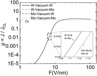
FIGURE 10. The normalized electron emission current density (μ) versus the applied electric field value (F) for four different nano-gap configurations including W-vacuum-W, W-vacuum-Mo, Mo-vacuum-W and Mo-vacuum-Mo. All calculations are performed for nanogap spacing fixed to 1 nm.
Lastly, we expand the use of current algorithm for characterizing the electron field emission properties with the quantum many-body effects of space charges from the 1-D model to the 3-D metal nano-emitters. To further investigate the quantum effects of space charge on three-dimensional electron field emission under a nanogap, we performed electrodynamics coupled molecular dynamics with particle-in-cell simulations (ED-MD-PIC) [45–47] for a copper tip (D = 10 nm, r = 1 nm, h = 100 nm) under an electric voltage of 30 V and gap spacing 10 nm or 3 GV/m. All numerical calculations are conducted using the in-house code named FEcMD software [31]. Specifically, as shown in Figure 11, we construct a cathode nano-tip with a total length of 100 nm. To save computational time, the nano-tip is divided into two parts. The upper half part enclosed by the box represents atomic structure of the apex which is subjected to the molecular dynamics simulation dynamically coupled with the electrodynamics. Otherwise, the lower half coarse-grained section is treated as an extended base, serving as boundary conditions for charge continuity and heat balance equations. In the finite element calculation, the initial distance between the lower nano-tip and the upper anode is set to 10 nm. The Dirichlet boundary condition is applied to the anode with φ = 30 V. The initial temperature of nano-tip is set to 300 K. The standard LIBXC library [29] is interfaced with FEcMD software to treat exchange-correlation effects of space charges at various levels on the Jacob’s ladder of density functionals, including PW-LDA, PZ-LDA, PBE and SCAN functionals in this paper [23, 38–41].
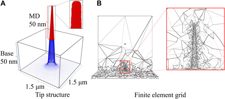
FIGURE 11. Multi-scale atomic structure and finite element mesh grids of nano-emitter in 3-D field emission calculations: (A): The typical initial configuration of metal nano-emitter consists of a coarse-grained stand (the blue region enclosed by black box) and the realistic atomic structure of apex (All atoms are represented by small red balls); (B): multi-scale finite element mesh grids of physical fields.
In the current implementation of WKBJ model to evaluate the electron emission for 3-D nano-tip, the electric field is calculated on the finite-element grid, and the emitted electron trajectory is aligned in the direction of electric field that is normal to emission surface. The quasi-planar emitter is adopted locally to calculate the electric field value locally, and to obtain the emission current density. This procedure is regarded as a valid approximation for computing the field emission characteristics of nano-emitter within a relatively large spacing with anode.
In Figures 12A,B, distributions of space charge density and the corresponding exchange-correlation potential are mapped on the apex of nano-emitter. The simulations reveal that the space charges emitted into the vacuum are non-uniformly accumulated near the top of the nano-emitter because of the high local E-field strength in the same region. The strong exchange-correlation effects are clearly seen in the area where the space charge density is high on the apex of nano-emitter. Figure 12C shows the 1-D electron transmission potential barrier profile perpendicular to the emission surface on a position with the maximum local E-field value at the apex of the nano-tip. After considering the exchange-correlation effects of space charges, the transmission barrier height is lowered, compared to that of without including such effects. Therefore, the field emission process on the nano-emitter is enhanced. Otherwise, the employed exchange-correlation functionals behavior differently for decreasing the electron transmission barrier on a nano-emitter. The barrier height is lowered most by using PW-LDA with Slater exchange method. Meanwhile, PZ with Slater exchange, PBE and SCAN functionals give almost identical barrier profiles shown in Figure 12C.
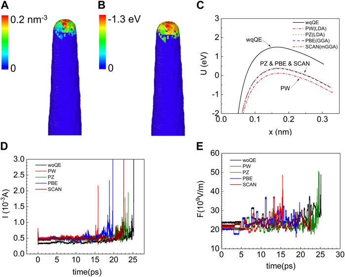
FIGURE 12. The 3-D ED-MD-PIC simulations for electron emission process of the conical metal nano-emitter (r = 1 nm, h = 100 nm) with an voltage of 30 V applied to a nano-gap of 10 nm at the beginning: (A) The space charge density distribution near the surface of the nano-tip; (B) The distribution of exchange-correlation potential in the same region calculated from SCAN; (C) The electron transmission barrier height profiles for PW-LDA, PZ-LDA, PBE and SCAN functionals and without considering the quantum-many body effects (woQE); (D) The total emission current versus the time; (E) The maximum local E-field value versus the time.
Certainly, the enhanced electron field emission process directly affects the local E-field evolution on the apex region of metal nano-emitter during the ED-MD-PIC simulation. In Figures 12D,E, we compare the calculated total field emission current and the local E-field strength of nano-emitter during the whole ED-MD-PIC simulation. The large sparks observed in Figures 12D,E after running simulations for certain times within different treatment of the quantum many-body effects of space charges are an indication of electric pre-breakdown caused by structural failure [32–34]. In Figure 12D, it is found that the initial emission current is highest for PW-LDA method, and the other three exchange-correlation functionals output very similar results. The lowest emission current is obtained without including the exchange-correlation effects at all in the WKBJ method. As a result, the obtained local E-field value has the highest value initially in ED-MD-PIC simulation due to the least space charge screening effect, as shown in Figure 12E. The field emission process leads to the Joule heating and Nottingham heating (cooling) mechanisms that critically determine the atomic structural evolution of metal nano-emitter in MD simulation. The fluctuations seen in Figure 12 for either total emission current or E-field value reflect the changes in atomic structure, shape, and geometries of nano-emitter under the electric stress, thermal stress, and interatomic interactions in typical ED-MD-PIC simulation [32–34].
Finally, it is worth noting that Cabrera and coworkers systematically studied the current versus voltage characteristics of a diode-like tunnel junctions consisting of a sharp W cathode and a planar electrode as the electron collector with the typical nanogap spacing spanning from 3 nm to 300 nm and the applied voltage between 10 V and 80 V [48]. On the other hand, the field induced phase transitions in Si nanotip have been experimentally investigated using the transmission electron microscopy in situ at the relatively low electric field (0.6–1.65 V/nm) and with the gap distance about several hundred nanometers (200–500 nm) [49]. Clearly, the methodology developed in the current paper could be very helpful to understand experimental works on the electron field emission characteristics and atomic structure evolutions in the nanogaps with different spacings and the applied voltages in the future works.
In this paper, we consider the image charge potential (anode screening effect), space charge Coulomb potential and exchange-correlation effect at the same time for one-dimension metal-vacuum-metal filed emission model. By self-consistently solving the one-dimensional Poisson-Schrödinger equation in the combination with WKBJ model in metal-vacuum-metal nanogap, four different electron emission regimes are defined and characterized, including the quantum regime (QR), the space charge limited regime (SCLR), the direct tunnelling regime (DTR) and the classic field emission regime (FER). In the QR, the quantum effects in terms of exchange-correlation potential of space charges have a significant effect on the emission current, and which could increase the emission current density above the limits of the classical CL law in nanogap. In addition, the use of different exchange-correlation density functionals also impact the predicted emission current density in the QR. Besides, to investigate the impact of different electrode materials on field emission, we performed simulations for W and Mo as electrode materials, finding that the property of cathode materials determined the emission current density. Finally, to investigate the quantum effects on thermal runaway, three-dimensional ED-MD-PIC simulations were performed with different exchange-correlation functionals for a nano-tip under a gap of 10 nm with 30 V. The quantum effects with different exchange-correlation functionals also impact the current and maximum E-field value at initial and pre-breakdown time. Overall, recognizing different electron field emission regimes is vital to understand the field emission characteristics of nanogap in modern field emission devices.
The original contributions presented in the study are included in the article/supplementary material, further inquiries can be directed to the corresponding authors.
NL contributed to the whole simulations, achievement of the numerical solving of Poisson-Schrödinger coupled equations, results analysis and original draft writing. YC and KW provided valuable guidance for this work. BX gave the key suggestions for this work, reviewd and edited the draft writing. All authors contributed to the article and approved the submitted version.
This research is financially supported by Young Talent Support Plan at Xi’an Jiao-tong University awarded to BX with the contract No: DQ1J009.
The authors declare that the research was conducted in the absence of any commercial or financial relationships that could be construed as a potential conflict of interest.
All claims expressed in this article are solely those of the authors and do not necessarily represent those of their affiliated organizations, or those of the publisher, the editors and the reviewers. Any product that may be evaluated in this article, or claim that may be made by its manufacturer, is not guaranteed or endorsed by the publisher.
1. Chen SC, Feng Z, Li J, Tan W, Du LH, Cai JW, et al. Ghost spintronic THz-emitter-array microscope. Light Sci Appl (2020) 9:99. doi:10.1038/s41377-020-0338-4
2. Deka N, Subramanian V. On-Chip fully integrated field emission arrays for high-voltage MEMS applications. IEEE Trans Electron Devices (2020) 67:3753–60. doi:10.1109/Ted.2020.3006167
3. Zhang J, Zhang D, Fan YW, He JT, Ge XJ, Zhang XP, et al. Progress in narrowband high-power microwave sources. Phys Plasma (2020) 27. doi:10.1063/1.5126271
4. Laszczyk K, Krysztof M. Electron beam source for the miniaturized electron microscope on-chip. Vac (2021) 189:110236. doi:10.1016/j.vacuum.2021.110236
5. El-Gomati MM, Wells T, Zha XP, Sykes R, Russo CJ, Henderson R, et al. 100 keV vacuum sealed field emission gun for high resolution electron microscopy. J Vac Sci Technol B (2021) 39:062804. doi:10.1116/6.0001275
6. Laszczyk KU. Field emission cathodes to form an electron beam prepared from carbon nanotube suspensions. Micromachines (2020) 11:260. doi:10.3390/mi11030260
7. Patra A, More MA, Late DJ, Rout CS. Field emission applications of graphene-analogous two-dimensional materials: Recent developments and future perspectives. J Mater Chem C (2021) 9:11059–78. doi:10.1039/d1tc02054d
8. Di Bartolomeo A, Pelella A, Urban F, Grillo A, Iemmo L, Passacantando M, et al. Field emission in ultrathin PdSe2 back-gated transistors. Adv Electron Mater (2020) 6:2000094. doi:10.1002/aelm.202000094
9. Gee A, Jaafar AH, Brachnakova B, Massey J, Marrows CH, Salitros I, et al. Multilevel resistance switching and enhanced spin transition temperature in single- and double-molecule spin crossover nanogap devices. J Phys Chem C (2020) 124:13393–9. doi:10.1021/acs.jpcc.0c03824
10. Adam T, Dhahi TS, Gopinath SCB, Hashim U, Uda MNA. Recent advances in techniques for fabrication and characterization of nanogap biosensors: A review. Biotechnol Appl Biochem (2022) 69:1395–417. doi:10.1002/bab.2212
11. Al-Tabbakh AA, Madanat MA, Mousa MS. Application of fractional Fowler-Nordheim law on field electron emission from tungsten and lanthanum hexaboride nano-scale emitters. Philos Mag (2023) 103:860–71. doi:10.1080/14786435.2023.2173366
12. Karmakar S, Parey V, Mistari CD, Thapa R, More MA, Behera D. Fowler-nordheim law correlated with improved field emission in self-assembled NiCr2O4 nanosheets. Phys Status Solidi A (2020) 217:1900741. doi:10.1002/pssa.201900741
13. Al-Tabbakh AA. The behavior of Fowler-Nordheim plot from carbon nanotubes-based large area field emitters arrays. Ultramicroscopy (2020) 218:113087. doi:10.1016/j.ultramic.2020.113087
14. Zhou Y, Zhang P. Theory of field emission from dielectric coated surfaces. Phys Rev Res (2020) 2:043439. doi:10.1103/PhysRevResearch.2.043439
15. De Rose LB, Scherer A, Jones WM. Suspended nanoscale field emitter devices for high-temperature operation. IEEE Trans Electron Devices (2020) 67:5125–31. doi:10.1109/Ted.2020.3019765
16. Fowler RH, Nordheim L. Electron emission in intense electric fields. Proc R Soc London, Ser A (1928) 119:173–81. doi:10.1098/rspa.1928.0091
17. Child CD. Discharge from hot CaO. Phys Rev (1911) 32:0492–511. doi:10.1103/PhysRevSeriesI.32.492
18. Koh WS, Ang LK. Quantum model of space-charge-limited field emission in a nanogap. Nanotechnol (2008) 19:235402. doi:10.1088/0957-4484/19/23/235402
19. Simmons JG. Generalized formula for the electric tunnel effect between similar electrodes separated by a thin insulating film. J Appl Phys (1963) 34:1793–803. doi:10.1063/1.1702682
20. Lau YY, Chernin D, Colombant DG, Ho PT. Quantum extension of Child-Langmuir law. Phys Rev Lett (1991) 66:1446–9. doi:10.1103/PhysRevLett.66.1446
21. Ang LK, Kwan TJT, Lau YY. New scaling of Child-Langmuir law in the quantum regime. Phys Rev Lett (2003) 91:208303. doi:10.1103/PhysRevLett.91.208303
22. Koh WS, Ang LK. Transition of field emission to space-charge-limited emission in a nanogap. Appl Phys Lett (2006) 89:183107. doi:10.1063/1.2378405
23. Perdew JP, Wang Y. Accurate and simple analytic representation of the electron-gas correlation-energy. Phys Rev B (1992) 45:13244–9. doi:10.1103/PhysRevB.45.13244
24. Perdew JP, Burke K, Wang Y. Generalized gradient approximation for the exchange-correlation hole of a many-electron system. Phys Rev B (1996) 54:16533–9. doi:10.1103/PhysRevB.54.16533
25. Wang YA, Carter EA. Orbital-free kinetic-energy density functional theory. Theor Methods Condens Phase Chem (2002) 117–84. doi:10.1007/0-306-46949-9_5
26. Kyritsakis A, Djurabekova F. A general computational method for electron emission and thermal effects in field emitting nanotips. Comput Mater Sci (2017) 128:15–21. doi:10.1016/j.commatsci.2016.11.010
27. Kemble EC. A contribution to the theory of the BWK method. Phys Rev (1935) 48:549–61. doi:10.1103/PhysRev.48.549
28. Il'chenko LG, Goraychuk TV. Role of the image forces potential in the formation of the potential barrier between closely spaced metals. Surf Sci (2001) 478:169–79. doi:10.1016/S0039-6028(01)00844-5
29. Marques MAL, Oliveira MJT, Burnus T. Libxc: A library of exchange and correlation functionals for density functional theory. Comput Phys Commun (2012) 183:2272–81. doi:10.1016/j.cpc.2012.05.007
30. Miller SC, Good RH. A wkb-type approximation to the schrodinger equation. Phys Rev (1953) 91:174–9. doi:10.1103/PhysRev.91.174
31. Li N, Gao XY, Feng XH, Wu K, Cheng YH, Xiao B. FEcMD: A multi-physics and multi-scale computational program for electron emission characteristics dynamically coupled with atomic structure in metal nano-emitters. Comput Phys Commun (2023).
32. Gao XY, Li N, Song ZF, Wu K, Cheng YH, Xiao B. Atomic structure evolution and linear regression fitting models for pre-breakdown electric field strength of FCC, BCC and HCP metal nano-emitters under high electric field from PIC-ED-MD simulations. J Phys D: Appl Phys (2023) 56:265203. doi:10.1088/1361-6463/acc7b2
33. Gao XY, Kyritsakis A, Veske M, Sun WJ, Xiao B, Meng GD, et al. Molecular dynamics simulations of thermal evaporation and critical electric field of copper nanotips. J Phys D: Appl Phys (2020) 53:365202. doi:10.1088/1361-6463/ab9137
34. Gao XY, Li N, Kyritsakis A, Veske M, Dong CY, Wu K, et al. Structural evolution and thermal runaway of refractory W and Mo nanotips in the vacuum under high electric field from PIC-ED-MD simulations. J Phys D: Appl Phys (2022) 55:335201. doi:10.1088/1361-6463/ac7177
35. Skriver HL, Rosengaard NM. Surface-energy and work function of elemental metals. Phys Rev B (1992) 46:7157–68. doi:10.1103/PhysRevB.46.7157
36. Luginsland JW, Lau YY, Umstattd RJ, Watrous JJ. Beyond the Child-Langmuir law: A review of recent results on multidimensional space-charge-limited flow. Phys Plasma (2002) 9:2371–6. doi:10.1063/1.1459453
37. Toijala H, Eimre K, Kyritsakis A, Zadin V, Djurabekova F. Ab initio calculation of field emission from metal surfaces with atomic-scale defects. Phys Rev B (2019) 100:165421. doi:10.1103/PhysRevB.100.165421
38. Dirac PAM. Note on exchange phenomena in the Thomas atom. Proc Cambridge Philos Soc (1930) 26:376–85. doi:10.1017/S0305004100016108
39. Perdew JP, Zunger A. Self-interaction correction to density-functional approximations for many-electron systems. Phys Rev B (1981) 23:5048–79. doi:10.1103/PhysRevB.23.5048
40. Perdew JP, Burke K, Ernzerhof M. Generalized gradient approximation made simple. Phys Rev Lett (1996) 77:3865–8. doi:10.1103/PhysRevLett.77.3865
41. Sun JW, Ruzsinszky A, Perdew JP. Strongly constrained and appropriately normed semilocal density functional. Phys Rev Lett (2015) 115:036402. doi:10.1103/PhysRevLett.115.036402
42. Bartok AP, Yates JR. Regularized SCAN functional. J Chem Phys (2019) 150:161101. doi:10.1063/1.5094646
43. Furness JW, Kaplan AD, Ning JL, Perdew JP, Sun JW. Accurate and numerically efficient r(2)SCAN meta-generalized gradient approximation. J Phys Chem Lett (2020) 11:8208–15. doi:10.1021/acs.jpclett.0c02405
44. Jensen KL. Erratum: “Exchange-correlation, dipole, and image charge potentials for electron sources: Temperature and field variation of the barrier height” [J. Appl. Phys. 85, 2667 (1999)]. J Appl Phys (2000) 88:4455–6. doi:10.1063/1.1289819
45. Djurabekova F, Parviainen S, Pohjonen A, Nordlund K. Atomistic modeling of metal surfaces under electric fields: Direct coupling of electric fields to a molecular dynamics algorithm. Phys Rev E (2011) 83:026704. doi:10.1103/PhysRevE.83.026704
46. Parviainen S, Djurabekova F, Pohjonen A, Nordlund K. Molecular dynamics simulations of nanoscale metal tips under electric fields. Nucl Instrum Methods Phys Res Sect B (2011) 269:1748–51. doi:10.1016/j.nimb.2010.12.058
47. Parviainen S, Djurabekova F, Timko H, Nordlund K. Electronic processes in molecular dynamics simulations of nanoscale metal tips under electric fields. Comput Mater Sci (2011) 50:2075–9. doi:10.1016/j.commatsci.2011.02.010
48. Cabrera H, Zanin DA, De Pietro LG, Michaels T, Thalmann P, Ramsperger U, et al. Scale invariance of a diodelike tunnel junction. Phys Rev B (2013) 87:115436. doi:10.1103/PhysRevB.87.115436
49. Huang YF, Deng ZX, Wang WL, Liang CL, She JC, Deng SZ, et al. Field-induced crystalline-to-amorphous phase transformation on the Si nano-apex and the achieving of highly reliable Si nano-cathodes. Sci Rep (2015) 5:10631. doi:10.1038/srep10631
For the one-dimensional Poisson-Schrödinger as shown in Equations (7) and (8), we employed FDM for discretization and solution:
Regarding all the integral formulas mentioned in the paper, such as the integral terms in Equations (1), (4), and (6), we adopted the classical formula with equidistant abscissas for discrete integration. To enhance computational accuracy, the extended Simpson’s rule was utilized to solve the integral terms.
Here, f (x) represents the integrand, and N denotes the number of points determined by the user. Typically, a higher number of points leads to more accurate integration results but requires more computation time. To achieve a good balance between computational efficiency and accuracy, we chose N = 200 points for the integration calculations.
Notably, the current methodology allows us to explore different electron field emission regimes within the same set of equations. Each component in the space charge fields can be employed in the calculation, and its influences on the electron emission properties in nanogap can be investigated. It is also worth mentioning that one may recast the equations A1 and A2 into a single time-independent Schrödinger equation by ignoring both space charge Hartree potential (φsc) and exchange-correlation effects (φxc). This corresponds to the field emission process without considering any space charge fields (φsc and φxc).
Keywords: nano-gap, electron field emission, space charge effect, exchange-correlation potential, exchange-correlation functional
Citation: Li N, Wu K, Cheng Y and Xiao B (2023) Self-consistent numerical solution of quantum regime with exchange-correlation effects of space charges for electron field emission in a nano-gap. Front. Phys. 11:1223704. doi: 10.3389/fphy.2023.1223704
Received: 16 May 2023; Accepted: 18 July 2023;
Published: 25 July 2023.
Edited by:
Shuqun Wu, Nanjing University of Aeronautics and Astronautics, ChinaReviewed by:
Daniel Moraru, Shizuoka University, JapanCopyright © 2023 Li, Wu, Cheng and Xiao. This is an open-access article distributed under the terms of the Creative Commons Attribution License (CC BY). The use, distribution or reproduction in other forums is permitted, provided the original author(s) and the copyright owner(s) are credited and that the original publication in this journal is cited, in accordance with accepted academic practice. No use, distribution or reproduction is permitted which does not comply with these terms.
*Correspondence: Yonghong Cheng, Y3loQG1haWwueGp0dS5lZHUuY24=; Bing Xiao, YmluZ3hpYW84NEB4anR1LmVkdS5jbg==
Disclaimer: All claims expressed in this article are solely those of the authors and do not necessarily represent those of their affiliated organizations, or those of the publisher, the editors and the reviewers. Any product that may be evaluated in this article or claim that may be made by its manufacturer is not guaranteed or endorsed by the publisher.
Research integrity at Frontiers
Learn more about the work of our research integrity team to safeguard the quality of each article we publish.