 Ali Deniz Özdemir
 Fabian Li1
 Franz Symalla
 Wolfgang Wenzel
- 1Institute of Nanotechnology, Karlsruhe Institute of Technology (KIT), Karlsruhe, Germany
- 2Nanomatch GmbH, Karlsruhe, Germany
Simulations have become increasingly important to understand and design organic optoelectronic devices, such as organic light emitting diodes (OLEDs) and to optimize their performance by selecting appropriate materials and layer arrangements. To achieve accurate device simulations, it is crucial to consider the interplay between material properties, device architecture, and operating conditions and to incorporate physical processes such as charge injection, transport, recombination, and exciton decay. Simulations can provide insights into device bottlenecks and streamline optimization cycles, eliminating the need for physical prototyping and rationalizing OLED design. In this study, we investigated three heuristic OLED architectures with a 3D kinetic Monte Carlo (kMC) model and compared their quantum efficiency at different operation voltages. Our investigation focused on examining the effects of various layer arrangements on charge and exciton dynamics in OLED devices and establishing design principles for achieving high efficiency, which are consistent with experimental observations. Notably, we find that increasing the thickness of the emissive layer (EML) led to higher luminance efficiency, and that an emitter concentration of approximately 5% results in optimal performance. By using this model, it is possible to rapidly study the influence of many device parameters and explore a broad range of parameter and architecture space within a reasonable time-frame.
1 Introduction
Nowadays, Organic Light Emitting Diodes (OLEDs) are widely used in modern applications such as displays and general lighting [1–4]. These devices are composed of multiple layers of organic thin films, each having a specific role [5]. To achieve high efficiency in an OLED, it is crucial that each electron-hole pair injection leads to recombination on an emitter molecule in the emissive layer followed by radiative decay. However, the efficiency can be reduced by various physical processes that occur on different time and length scales. To improve OLED efficiency, it is essential to optimize the interplay between the different layers and physical processes, such as charge injection, transport, recombination, and exciton decay. Careful selection of materials and layer arrangements can minimize loss mechanisms and maximize quantum efficiency. Computational simulations have become a powerful tool for optimizing OLED performance by efficiently exploring a large parameter space and providing insights into complex processes occurring on various scales [6–12].
The objective of this work is to assess the effect of integrating charge injection and blocking layers [13] in the context of a mesoscopic OLED model using a 3D kinetic Monte-Carlo (kMC) approach [6, 14]. The aim is to evaluate the impact of each layer on significant performance parameters, such as charge balance, exciton generation, and the occurrence of quenching events, including exciton-polaron quenching [15, 16] and exciton-exciton annihilation [17, 18].
This analysis will help determine the influence of these factors on the internal quantum efficiency (IQE), which is a crucial metric for assessing OLED efficiency. Furthermore, we optimize the device by varying parameters such as the emissive layer (EML) thickness and emitter concentration.
2 Materials and methods
Using the LightForge kMC simulation package [6], we model the injection and transfer of charge, formation of excitons, their radiative and thermal decay, and bimolecular quenching [18]. To investigate three different device architectures, depicted in Figure 1, we employ a heuristic model, similar to previous studies [7]. Further details on the simulation setup and process-rate calculations are provided below.
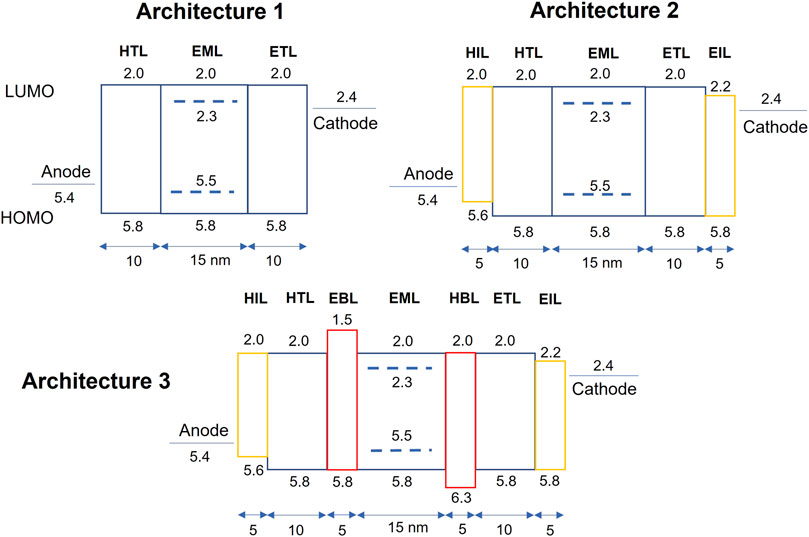
FIGURE 1. Schematic representation of the devices studied in this work. The first device (A1) consists of three layers, where the hole transport (HTL) and electron transport layers are of equal thickness and energy levels. The anode injects holes into the HTL, while electrons are injected from the cathode to the electron transport layer (ETL). Holes travel from the HTL towards the emissive layer (EML), where emitter molecules with high phosphorescent emission rates and lower HOMO-LUMO gap are blended to promote exciton generation near the emitter molecules. The energy levels of the emitter are indicated by the dashed lines, and the layer thickness is given in nanometers (nm). Architecture 2 (A2) is similar to A1 but includes additional hole and electron injection layers (shown in yellow). Architecture 3 (A3) has an additional two blocking layers sandwiching the EML to restrict charge carriers to the EML.
2.1 Virtual device setup
In our approach we model OLED devices as a series of layers, each comprising a 3D cubic lattice with a lattice constant of a = 1 nm. At each lattice site i, we assign HOMO and LUMO energy levels, denoted by
We categorize molecules or sites into two groups: phosphorescent emitters and non-emitters. This differentiation is important for modeling various excitonic processes such as inter-system crossing (ISC) and radiative decay of singlets or triplets, and it is based on the exciton parameters of each type, which are described in greater detail in the Supplementary Material. Notably, the materials used for charge-injection, transport, and blocking layers are all non-emissive. In contrast, emitters are blended with non-emitting host molecules within the emissive layer (EML).
2.2 Charge injection
Charge injection from an electrode to an organic molecule is treated as a distinct process, where a charge carrier transitions from a continuous bath of charges in the electrode to a specific organic site i with an associated energy level (
where the temperature is T = 300 K in all our simulations. Here, JXi denotes the electronic coupling between the electrode X and the organic molecule i. The injection barrier for holes (X = A, for anode) is given by:
where
where the dielectric constant ϵr was 4.0 for all layers. The dynamic electrostatic potential is computed by using the Ewald method [21].
The injection barrier for electrons at the cathode (X = C) is defined in a similar manner:
2.3 Charge transport
Charge transport in organic semiconductors is commonly modelled as hopping transport [12, 22, 23], where a charge carrier hops from one site to another. The hopping rate between sites i and j is described by Marcus theory [24], which takes into account the reorganization energy λ and the energy difference ΔEij. The latter includes the change in the dynamic Coulomb potential ϕD resulting from the hop and the applied electric field:
where the electronic coupling Jij is given by:
The maximum coupling j0 and decay length δ0 are specified in the Supplementary Material.
2.4 Excitonic processes
Excitons occur either as singlets or triplets. We limit the number of excited states to one per spin multiplicity and define the excitation energy
where EB is the exciton binding-energy and EST the singlet-triplet gap.
2.4.1 Exciton recombination and charge separation
If there is an exciton located at a given site i, it can undergo charge separation by following two distinct pathways: hole separation, which involves the transfer of the hole to a neighboring site, leaving the electron behind at site i, or electron separation, which works in a similar way, but with the electron moving to a neighboring site instead. In our model, we describe separation as a charge transfer process, and the energy barrier for hole separation is determined by:
where Φi(j) is the total electrostatic potential at site i (j) and the Coulomb potential between the charged sites i and j is explicitly taken into account.
The energy barrier for the electron separation process is given by:
2.4.2 Exciton transfer
Excitons can undergo transport through two mechanisms: Dexter transfer [25, 26], where the bounded electron-hole pair jumps to an adjacent site by simultaneous charge transfer, and Förster transfer [27, 28], where the energy is transferred via a virtual photon. Both processes are included in our kMC model.
Since Dexter-transfer involves the simultaneous transfer of the electron and hole comprising the exciton, we employ the Marcus rate expression (Eq. 5) to calculate Dexter transfer rates. However, there are certain modifications: we utilize the excitation energies
In our model, Marcus theory is also used to compute the Förster transfer rates, incorporating the long-range coupling that is specific to Förster transfer:
where
Further details regarding the modeling of transition dipole moments can be found in the Supplementary Material.
2.4.3 Excitonic quenching
Excitons suffer from quenching through various processes such as triplet-triplet annihilation (TTA) or triplet-polaron quenching (TPQ) [18, 30–34]. In this study, we focus on modeling the rates of TTA and TPQ using a heuristic formula for quenching of type Q = TTA or TPQ:
As these quenching processes are based on Förster mechanisms, the distance dependence of the quenching rates follows the same law as that of Förster-based exciton transfer
2.4.4 Radiative and thermal decay
The rates for thermal or radiative decay is the inverse of the corresponding lifetime. The lifetimes for all material types are given in the Supplementary Material.
2.5 Simulation details
To obtain reliable results, we ran simulations for 20 replicas of each device, with each replica undergoing 50 million kMC steps. Properties as current- or particle-densities are then averaged over all replicas. The simulated devices were modeled with a cross section of 20 × 20 nm2. To assess the adequacy of this size, we conducted additional simulations with larger cross sections, specifically 50 × 50 nm2, and compared the resulting charge carrier profiles (see Supplementary Figure S1). From this comparison, we concluded that the chosen cross-sectional area of 20 × 20 nm2 was sufficient to qualitatively capture the charge carrier distributions and other particle events.
The built-in electric field of the devices is determined by the equation:
where e represents the elementary charge. The distance between the anode and the organic material is 0.8 nm for both the anode and cathode, taking into account the surface roughness of the amorphous organic layer with typical molecules having a volume of approximately 1 nm3. The total thickness of all organic layers is denoted by LDevice. To apply electric fields that exceed the built-in field, we use the following scheme:
where Fx takes on values from 0.01 to 0.06 V nm−1 unless otherwise specified.
We define the IQE as:
where Nrad denotes the number of emitted photons, NX the total number of excitons, and NCS represents the number of charge separations. Additional information about the rates used in the kMC simulations can be found in the Supplementary Material.
3 Results and discussion
3.1 Comparison of three device architectures
We conducted simulations of charge and exciton dynamics in the three architectures presented in Figure 1. Our aim was to compare the IQE of the three devices and examine the charge, exciton, and quenching profiles along the transport axis of the devices. This visualization allowed us to observe the impact of architectural differences on the carrier and exciton dynamics.
3.1.1 IV and IQE characteristics
As described in the methodology section, we performed simulations by applying electric fields that counterbalance the built-in field FBI of each device, so that the effective field experienced by the charge carriers is equal in all devices. Figure 2A displays the current-voltage characteristics that resulted from the simulations of all device architectures (A1-A3) with an emitter concentration of 15%. It is important to note that, despite the identical effective fields experienced by the charge carriers, there is a significant difference in the currents between A2 or A3 and A1, which varies by approximately one order of magnitude. The reason for this difference is that A2 and A3 contain a higher number of layers than A1, resulting in a higher effective resistance that requires a larger electric field (or voltage) to generate the same currents. Additionally, the presence of blocking layers in A3 causes a further reduction in the achieved current when compared to A2. The impact of the difference in achieved current among the devices is reflected in their respective internal quantum efficiency. As the achieved currents decrease due to increased effective resistance, the roll-off effect is delayed, leading to higher IQEs at the same electric field experienced by the charge carriers. In Figure 2B, the IQEs of the devices are presented, with A2 and A3 exhibiting significantly larger IQEs at low currents. Conversely, A1 already achieves a current of approximately 103 mA/cm2 at the smallest electric field. Indeed, at high electric fields, the achieved currents of A2 and A3 become comparable to that of A1, and as a result, the roll-off effect becomes prominent, leading to a significant drop in IQE that is comparable to A1.

FIGURE 2. Panel (A) shows the IV curves of three devices, with A1 (blue), A2 (orange), and A3 (green). The thinnest device, A1, shows the highest current density, followed by A2 and then A3, which is the thickest. The increase in thickness results in higher resistance, leading to lower currents. (B) shows that A3 exhibits the highest IQE at low current densities (
It is evident that while the implementation of injection and blocking layers leads to a significant improvement in the IQE at low currents, which is in line with experimental findings [5, 13], all of the device architectures are still susceptible to roll-off, resulting in very small high-current IQEs.
3.1.2 Charge and exciton profiles
Figure 3 depicts the distribution of particles, such as charges and excitons, throughout the devices, represented by their profiles along the transport axis. Specifically, the charge carrier profile is determined by averaging the sum of all holes (or electrons) across the device’s cross-section at a given position along the transport axis over the simulation time. A value of 1 signifies that there is on average one hole (or electron) in the corresponding cross-sectional position. Upon analyzing the charge profile of A1 in Figure 3A, it becomes evident that the symmetry of A1 in terms of layer arrangement and energetic landscape is mirrored in the distribution of holes and electrons. The concentration of holes is observed to be high at the interface between the anode and the organic layer, decreasing towards the emissive layer and increasing again. A similar trend is observed for electrons, which are concentrated near the cathode-organic interface. Maintaining charge balance is essential for exciton generation, and A1 demonstrates good charge balance within the emissive layer, as reflected in the generation of excitons solely within that region (Figure 3B). The simulation results show that reducing charge balance, particularly in the transport layers and near the electrode interfaces, leads to a negligible number of excitons being generated over time. Figure 3C depicts the proportion of excitons per layer, quenched by TTA or TPQ or charge separation processes leading an exciton to an unbound electron-hole pair. All exciton quenching events and charge separation take place in the EML, indicating that the generated excitons do not leave the EML through diffusion processes.
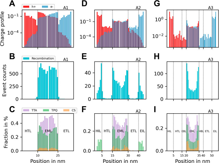
FIGURE 3. The particle profiles of devices with architectures A1, A2, and A3 are shown in the first, second, and third columns, respectively. We simulated one device for each architecture with an EML thickness of 15 nm and an emitter concentration of 15%, with the remaining layers as depicted in Figure 1. (A) displays the average number of electrons and holes per cross-sectional layer over the simulation time. We observe that the charge balance within the EML is not ideal, particularly at the interface to the transport layers where we have excess charges with an opposite sign. In (B), we observe that exciton generation only takes place inside the EML, despite non-zero charge balance throughout the entire transport axis. This is due to the relatively large HOMO-LUMO gap in the transport layers that suppresses charge recombination. (C) shows that in addition to TTA processes throughout the entire EML, excess charges at the interface to the transport layers lead to an increased number of TPQ processes, which negatively impacts the IQE. In (D), we add electron- and hole-injection layers (architecture A2) to slightly enhance the charge balance within the EML, but this causes exciton generation in the injection layers (E). This is due to the smaller HOMO-LUMO gap, despite the small but non-zero charge balance in the injection layers. As shown in (F), this leads to many TPQ events within the injection layers because of the combination of high exciton and charge density there. To prevent charges from recombining outside the EML, we add electron- and hole-blocking layers as depicted in Figure 1. As shown in (G), this causes the charge balance to vanish to the left and right of the EML. As expected, exciton generation only occurs within the EML (H). Furthermore, we observe a reduction in quenching throughout the device compared to (F) [panel (I)].
In Figure 3D, the addition of hole- and electron injection layers (A2) slightly increased the charge balance in the EML, but a significant amount of excitons was generated at the interface between the injection and transport layers. This is due to a smaller gap between HOMO and LUMO energies in the injection layers, which fosters exciton generation (Figure 3E). However, this effect is undesired because most of these excitons are unlikely to diffuse to the EML for radiative decay. Figure 3F shows that a large fraction of excitons undergo TTA and TPQ processes in the EML, while a significant fraction is quenched at the interface between the injection and transport layers. To prevent exciton generation at these positions, the charge balance outside the EML must be minimized by adding a hole or electron blocking layer on the left or right side of the EML. Figure 3G shows the charge profile of A3 with the desired absent charge balance outside the EML, resulting in exciton generation only inside the EML as seen in Figure 3H. However, the existence of blocking layers does not completely eliminate all bottlenecks. It results in the accumulation of excess holes at the interface between the emissive layer (EML) and the hole-blocking layer (HBL), as well as excess electrons at the interface between the EML and the electron-blocking layer (EBL). Furthermore, the concentration of charge carriers with opposite sign is higher at these interfaces compared to the central region of the EML. As a consequence, the large concentration of charge carriers contributes to a greater number of charge recombination and increases the occurrence of TPQ events (Figure 3I).
3.2 Varying emitter concentration
Figures 3C, F, and I provide insights into the particle dynamics resulting from the addition of injection and blocking layers. However, the high count of TTA and TPQ events, particularly at the interfaces with the blocking layers, remain a bottleneck. One potential strategy to address this issue is to decrease the exciton density in the EML by reducing the emitter concentration [35]. To explore this, we simulated A3 with varying emitter concentrations while keeping the rest of the device unchanged. Figure 4A presents the obtained IQE for A3 with emitter concentrations ranging from 1% to 15%. We observed an improvement for emitter concentrations below 15% for small current densities, but varying the emitter density could not prevent the roll-off effect, leading to low IQEs at large current densities. This is further illustrated in Figure 4B, where we plotted the difference of the IQEs at all applied electric fields relative to the 1% device IQE. We can clearly observe that, particularly for small fields (corresponding to small currents), the 15% device has up to 0.10 lower IQE. The device with 5% emitter concentration exhibited the best performance. Reineke and Baldo [36] reported that devices with emitter concentrations ranging from 1% to 10% exhibit high quantum efficiency, which our results support.
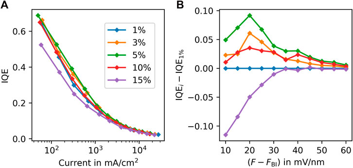
FIGURE 4. (A) The IQE versus current-density relationship for five devices with architecture A3 is presented. All devices have an EML thickness of 15 nm, but vary in emitter concentration from 1% to 15%. The optimal emitter concentration for low current densities appears to be around 5%, with a significant improvement in IQE compared to higher concentrations (15%). However, all devices suffer from significant roll-off, as evidenced by the sharp drop in IQE for high current densities. (B) Increasing the current-densities (corresponding to high electric fields) reduces the positive effect of optimizing the emitter concentration. This suggests that emitter concentration optimization alone can only improve device performance to a limited extent, but cannot overcome the drastic reduction in IQE caused by roll-off.
3.3 Varying EML thickness
Previous studies have reported that the efficiency of OLED devices is affected by the thickness of the emissive layer (EML), and thicker EMLs lead to more efficient devices [37, 38]. To verify this using our simulation model, we varied the EML thickness of architecture 3 with an emitter concentration of 15%. In Figure 5A, we present the IQE for architecture 3 with EML thicknesses ranging from 10 to 40 nm. Our simulations demonstrate that thicker EMLs result in higher IQE at low current densities, as observed in previous studies. For example, comparing the IQE of the 10 nm and 40 nm devices, we observe an improvement of about 0.3 (Figure 5B). Additionally, we find a significant improvement in the IQE for thicker emissive layers at high effective fields, indicating that increasing EML thickness not only improves the low-field IQE but also reduces roll-off, leading to more efficient devices across all operating regimes. To understand how EML thickness affects the quenching processes, similar to Figure 3I, we analyzed the ratio of triplet excitons undergoing TPQ or TTA quenching events. Figures 6A–C illustrate the quenching profiles of devices with architecture 3 and EML thicknesses of 10, 25, and 40 nm, respectively. All simulations were performed with an effective field of F − FBI = 60 mV/nm, leading to relatively high current densities (see Figure 5).
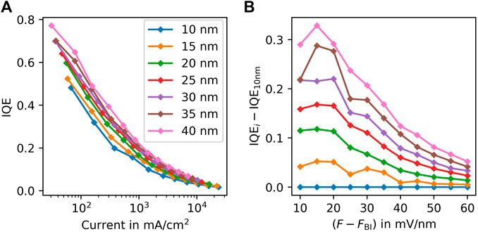
FIGURE 5. (A) IQE as a function of current-density for devices with architecture A3. This time, the emitter concentration is fixed at 15% for all devices, while the EML thickness varies from 10 nm to 40 nm. As the EML thickness increases, there is a significant improvement in IQE at low current-densities. However, roll-off still persists for large current-densities, but not as severe as observed in Figure 4. (B) To investigate the impact of varying EML thickness on the IQE at high fields (i.e., high current-densities), we plot the change in IQE with respect to the device with 10 nm EML thickness. Interestingly, we observe that the device with 40 nm EML thickness has approximately 8% higher IQE at 60 mV/nm compared to the thinnest device. Unlike optimizing emitter concentration, increasing the EML thickness has a positive effect on high-field IQE.
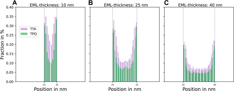
FIGURE 6. We present the quenching profiles of devices with architecture A3 having EML thicknesses of 10 nm (A), 25 nm (B), and 40 nm (C). It is observed that as the EML thickness increases, there is a decrease in the fraction of excitons generated per cross-sectional position that undergo TTA or TPQ. This decrease in quenching explains the increase in IQE for devices with higher EML thicknesses.
These results reveal that the fraction of TPQ and TTA events decreases with increasing EML thickness, leading to an increase in the IQE, as demonstrated in Figure 6. This demonstrates the ability of computational studies to provide insights into the relationship between modifications to device design that affect macroscopic properties such as IQE or emission, and microscopic properties such as particle dynamics. In conclusion, our simulations suggest that OLED devices with thicker EMLs are promising designs to reduce roll-off and increase internal quantum efficiency.
To strengthen our conclusions, we conducted simulations on 225 devices with architecture 3, where each device had a different EML thickness and emitter concentration. As depicted in Figure 7, the IQE exhibits a strong increasing trend when the EML thickness is increased while maintaining a constant emitter concentration at 5%–6%.
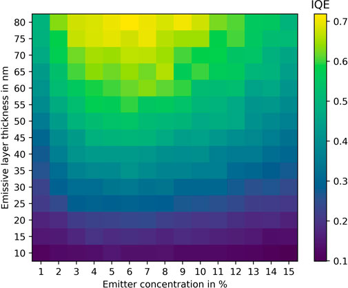
FIGURE 7. IQE of 225 devices with architecture A3 was simulated using an electric field of 30 mV/nm above the built-in field. The simulation results showed a consistent trend of increasing IQE with increasing EML thickness. Additionally, the optimal emitter concentration was found to be in the range of 5%–6%, which is consistent with previous findings.
4 Conclusion
In this research, we employed parametric kMC simulations to examine three different OLED architectures: A1, A2, and A3 (Figure 1), all of which had a phosphorescent emitter blended with the host material in the EML [39]. Our analysis revealed significant differences in device performance in terms of IQE and current-density behavior, as demonstrated in Figure 2. Using the particle profile plots presented in Figure 3, we were able to identify the main bottlenecks of each architecture. Specifically, we discovered that A1 suffered from non-ideal charge-balance within the EML, which resulted in enhanced TPQ, particularly at the interface to the transport layers, and a high number of TTA processes (Figure 3C) within the EML. To address this issue, we introduced charge injection layers between the electrodes and transport layers, which improved charge balance within the EML. However, this approach led to undesired exciton generation in the injection layers due to the small HOMO-LUMO gap, as shown in Figures 3E, F. While the addition of charge blocking layers helped to enhance the device efficiency, the roll-off effect remained severe.
For the multilayer architecture (A3), we further optimized the IQE by varying the emitter concentration and EML thickness (Figures 4, 5). Our simulations showed that low-current IQEs were highest for emitter concentrations around 5%, which is consistent with previously reported concentrations [35, 36]. However, the device still suffered from roll-off due to TTA and TPQ processes [40]. By increasing the EML thickness, we were able to further improve the efficiency and reduce the roll-off for current densities around 1 × 10⁴ mA/cm2.
Our calculations demonstrate that heuristic models can aid to analyze the device architecture and to identify parameters that affect efficiency. Our simulations pinpointed performance bottlenecks specific to each architecture, a task that would have been very time-consuming and expensive to achieve experimentally. We believe that our computational approach can help rationalize the design of efficient OLEDs by providing the flexibility to adjust material and device parameters to achieve high IQE, and by identifying performance bottlenecks a priori. Combining this approach with more realistic models based on ab initio data promises to increase the accuracy even more, but the computational cost of such models is high. For this reason, heuristic models can help to identify the most attractive regions in the design space for more detailed investigations.
Data availability statement
The raw data supporting the conclusion of this article will be made available by the authors, without undue reservation.
Author contributions
AÖ and FL contributed equally to this work. AÖ, FL, and WW conceived the idea and planned the theoretical calculations; FS wrote and improved simulation software for this work; AÖ and FL carried out the simulations; AÖ and FL prepared the manuscript with the inputs from all the co-authors and substantial revision from WW. All authors contributed to the article and approved the submitted version.
Funding
AÖ and FL received funding by GRK 2450 “Scale bridging methods in computational nanoscience.” WW acknowledges funding by the Deutsche Forschungsgemeinschaft (DFG) in the Research and Training Program “Tailored Scale Bridging Approaches to Computational Nanoscience” and under Germany’s Excellence Strategy—2082/1—390 761 711 (3DMM2O). We acknowledge support by the KIT-Publication Fund of the Karlsruhe Institute of Technology.
Conflict of interest
Author FS was employed by Nanomatch GmbH. WW holds shares of Nanomatch GmbH.
The remaining authors declare that the research was conducted in the absence of any commercial or financial relationships that could be construed as a potential conflict of interest.
Publisher’s note
All claims expressed in this article are solely those of the authors and do not necessarily represent those of their affiliated organizations, or those of the publisher, the editors and the reviewers. Any product that may be evaluated in this article, or claim that may be made by its manufacturer, is not guaranteed or endorsed by the publisher.
Supplementary material
The Supplementary Material for this article can be found online at: https://www.frontiersin.org/articles/10.3389/fphy.2023.1222589/full#supplementary-material
References
1. Huang Y, Hsiang EL, Deng MY, Wu ST. Mini-LED, micro-LED and OLED displays: Present status and future perspectives. Light: Sci Appl (2020) 9:105. doi:10.1038/s41377-020-0341-9
2. Prache O. Active matrix molecular OLED microdisplays. Displays (2001) 22:49–56. doi:10.1016/S0141-9382(00)00061-5
3. Salehi A, Fu X, Shin DH, So F. Recent advances in OLED optical design. Adv Funct Mater (2019) 29:1808803. doi:10.1002/adfm.201808803
4. Bauri J, Choudhary RB, Mandal G. Recent advances in efficient emissive materials-based OLED applications: A review. J Mater Sci (2021) 56:18837–66. doi:10.1007/s10853-021-06503-y
5. Negi S, Mittal P, Kumar B. Impact of different layers on performance of OLED. Microsystem Tech (2018) 24:4981–9. doi:10.1007/s00542-018-3918-y
6. Symalla F, Friederich P, Massé A, Meded V, Coehoorn R, Bobbert P, et al. Charge transport by superexchange in molecular host-guest systems. Phys Rev Lett (2016) 117:276803. doi:10.1103/PhysRevLett.117.276803
7. Özdemir AD, Kaiser S, Neumann T, Symalla F, Wenzel W. Systematic kMC study of doped hole injection layers in organic electronics. Front Chem (2022) 9:809415. doi:10.3389/fchem.2021.809415
8. Paterson L, May F, Andrienko D. Computer aided design of stable and efficient OLEDs. J Appl Phys (2020) 128:160901. doi:10.1063/5.0022870
9. Massé A, Friederich P, Symalla F, Liu F, Nitsche R, Coehoorn R, et al. Ab initio charge-carrier mobility model for amorphous molecular semiconductors. Phys Rev B (2016) 93:195209. doi:10.1103/physrevb.93.195209
10. Friederich P, Gómez V, Sprau C, Meded V, Strunk T, Jenne M, et al. Rational in silico design of an organic semiconductor with improved electron mobility. Adv Mater (2017) 29:1703505. doi:10.1002/adma.201703505
11. Feng X, Marcon V, Pisula W, Hansen MR, Kirkpatrick J, Grozema F, et al. Towards high charge-carrier mobilities by rational design of the shape and periphery of discotics. Nat Mater (2009) 8:421–6. doi:10.1038/nmat2427
12. Rühle V, Lukyanov A, May F, Schrader M, Vehoff T, Kirkpatrick J, et al. Microscopic simulations of charge transport in disordered organic semiconductors. J Chem Theor Comput (2011) 7:3335–45. doi:10.1021/ct200388s
13. Adamovich VI, Cordero SR, Djurovich PI, Tamayo A, Thompson ME, D’Andrade BW, et al. New charge-carrier blocking materials for high efficiency OLEDs. Org Electron (2003) 4:77–87. doi:10.1016/j.orgel.2003.08.003
14. Bässler H. Charge transport in disordered organic photoconductors a Monte Carlo simulation study. physica status solidi (b) (1993) 175:15–56. doi:10.1002/pssb.2221750102
15. Wehrmeister S, Jäger L, Wehlus T, Rausch AF, Reusch TC, Schmidt TD, et al. Combined electrical and optical analysis of the efficiency roll-off in phosphorescent organic light-emitting diodes. Phys Rev Appl (2015) 3:024008. doi:10.1103/PhysRevApplied.3.024008
16. Coehoorn R, Bobbert PA, van Eersel H. Forster-type triplet-polaron quenching in disordered organic semiconductors. Phys Rev B (2017) 96:184203. doi:10.1103/PhysRevB.96.184203
17. Engmann S, Barito AJ, Bittle EG, Giebink NC, Richter LJ, Gundlach DJ. Higher order effects in organic LEDs with sub-bandgap turn-on. Nat Commun (2019) 10:227. doi:10.1038/s41467-018-08075-z
18. Symalla F, Heidrich S, Friederich P, Strunk T, Neumann T, Minami D, et al. Multiscale simulation of photoluminescence quenching in phosphorescent OLED materials. Adv Theor Simulations (2020) 3:1900222. doi:10.1002/adts.201900222
19. Miller A, Abrahams E. Impurity conduction at low concentrations. Phys Rev (1960) 120:745–55. doi:10.1103/PhysRev.120.745
20. Kimber RGE, Wright EN, O’Kane SEJ, Walker AB, Blakesley JC. Mesoscopic kinetic Monte Carlo modeling of organic photovoltaic device characteristics. Phys Rev B (2012) 86:235206. doi:10.1103/PhysRevB.86.235206
21. Ewald PP. Die Berechnung optischer und elektrostatischer Gitterpotentiale. Annalen der Physik (1921) 369:253–87. doi:10.1002/andp.19213690304
22. Coropceanu V, Cornil J, da Silva Filho DA, Olivier Y, Silbey R, Brédas JL. Charge transport in organic semiconductors. Chem Rev (2007) 107:926–52. doi:10.1021/cr050140x
23. Kaiser S, Neumann T, Symalla F, Schlöder T, Fediai A, Friederich P, et al. De novo calculation of the charge carrier mobility in amorphous small molecule organic semiconductors. Front Chem (2021) 9:801589. doi:10.3389/fchem.2021.801589
24. Marcus RA. On the theory of oxidation-reduction reactions involving electron transfer. I. J Chem Phys (2004) 24:966–78. doi:10.1063/1.1742723
25. Köhler A, Bässler H. What controls triplet exciton transfer in organic semiconductors? J Mater Chem (2011) 21:4003–11. doi:10.1039/C0JM02886J
26. Zheng SW, Wang H, Wang L, Wang HY. Dexter-type exciton transfer in van der Waals heterostructures. Adv Funct Mater (2022) 32:2201123. doi:10.1002/adfm.202201123
27. Brixner T, Hildner R, Köhler J, Lambert C, Würthner F. Exciton transport in molecular aggregates – from natural antennas to synthetic chromophore systems. Adv Energ Mater (2017) 7:1700236. doi:10.1002/aenm.201700236
28. Wan Q, Li D, Zou J, Yan T, Zhu R, Xiao K, et al. Efficient long-range triplet exciton transport by metal–metal interaction at room temperature. Angew Chem Int Edition (2022) 61:e202114323. doi:10.1002/anie.202114323
29. Stehr V, Fink RF, Engels B, Pflaum J, Deibel C. Singlet exciton diffusion in organic crystals based on Marcus transfer rates. J Chem Theor Comput (2014) 10:1242–55. doi:10.1021/ct500014h
30. Kondakov DY. Triplet–triplet annihilation in highly efficient fluorescent organic light-emitting diodes: Current state and future outlook. Philos Trans R Soc A: Math Phys Eng Sci (2015) 373:20140321. doi:10.1098/rsta.2014.0321
31. Baldo MA, Adachi C, Forrest SR. Transient analysis of organic electrophosphorescence. II. Transient analysis of triplet-triplet annihilation. Phys Rev B (2000) 62:10967–77. doi:10.1103/PhysRevB.62.10967
32. van Eersel H, Bobbert PA, Janssen RAJ, Coehoorn R. Effect of Förster-mediated triplet-polaron quenching and triplet-triplet annihilation on the efficiency roll-off of organic light-emitting diodes. J Appl Phys (2016) 119:163102. doi:10.1063/1.4947457
33. Mesta M, van Eersel H, Coehoorn R, Bobbert PA. Kinetic Monte Carlo modeling of the efficiency roll-off in a multilayer white organic light-emitting device. Appl Phys Lett (2016) 108:133301. doi:10.1063/1.4945087
34. Lee J, Jeong C, Batagoda T, Coburn C, Thompson ME, Forrest SR. Hot excited state management for long-lived blue phosphorescent organic light-emitting diodes. Nat Commun (2017) 8:15566. doi:10.1038/ncomms15566
35. Murawski C, Leo K, Gather MC. Efficiency roll-off in organic light-emitting diodes. Adv Mater (2013) 25:6801–27. doi:10.1002/adma.201301603
36. Reineke S, Baldo MA. Recent progress in the understanding of exciton dynamics within phosphorescent OLEDs. physica status solidi (a) (2012) 209:2341–53. doi:10.1002/pssa.201228292
37. Höfle S, Lutz T, Egel A, Nickel F, Kettlitz SW, Gomard G, et al. Influence of the emission layer thickness on the optoelectronic properties of solution processed organic light-emitting diodes. ACS Photon (2014) 1:968–73. doi:10.1021/ph500186m
38. Bangsund JS, Hershey KW, Holmes RJ. Isolating degradation mechanisms in mixed emissive layer organic light-emitting devices. ACS Appl Mater Inter (2018) 10:5693–9. doi:10.1021/acsami.7b16643
39. Minaev B, Baryshnikov G, Agren H. Principles of phosphorescent organic light emitting devices. Phys Chem Chem Phys (2014) 16:1719–58. doi:10.1039/C3CP53806K
Keywords: OLED, computational design, kMC, organic semiconductor, roll-off
Citation: Özdemir AD, Li F, Symalla F and Wenzel W (2023) In silico studies of OLED device architectures regarding their efficiency. Front. Phys. 11:1222589. doi: 10.3389/fphy.2023.1222589
Received: 14 May 2023; Accepted: 26 July 2023;
Published: 07 August 2023.
Edited by:
Cina Foroutan-Nejad, Polish Academy of Sciences, PolandReviewed by:
Kun-Han Lin, Max Planck Institute for Polymer Research, GermanyBjörn Lüssem, University of Bremen, Germany
Copyright © 2023 Özdemir, Li, Symalla and Wenzel. This is an open-access article distributed under the terms of the Creative Commons Attribution License (CC BY). The use, distribution or reproduction in other forums is permitted, provided the original author(s) and the copyright owner(s) are credited and that the original publication in this journal is cited, in accordance with accepted academic practice. No use, distribution or reproduction is permitted which does not comply with these terms.
*Correspondence: Wolfgang Wenzel, d29sZmdhbmcud2VuemVsQGtpdC5lZHU=