 Talia Tene1Marco Guevara2Myrian Borja3María José Mendoza Salazar4María de Lourdes Palacios Robalino4
 Cristian Vacacela Gomez5*
 Stefano Bellucci5
- 1Department of Chemistry, Universidad Técnica Particular de Loja, Loja, Ecuador
- 2UNICARIBE Research Center, University of Calabria, Rende, Italy
- 3Facultad de Ciencias, Escuela Superior Politécnica de Chimborazo (ESPOCH), Riobamba, Ecuador
- 4Carrera de Matemática, Facultad de Ciencias, Escuela Superior Politécnica de Chimborazo (ESPOCH), Riobamba, Ecuador
- 5INFN-Laboratori Nazionali di Frascati, Frascati, Italy
Silicene nanostrips (SiNSs) have garnered significant attention due to their remarkable physical properties, making them an ideal candidate for numerous electronics and plasmonics applications. Their compatibility with current semiconductor technology further enhances their potential. This study aims to investigate the electronic and plasmonic properties of SiNSs with a minimum width of 100 nm using a semi-analytical model that utilizes the carrier velocity of silicene. The carrier velocity was calculated using density functional computations and refined through the GW approximation. Our results reveal that SiNSs with widths ranging from 100 to 500 nm exhibit small bandgaps within the range of a few meV, specifically ranging from 30 to 6 meV, respectively. Furthermore, all the nanostrips analyzed in this study exhibit a
1 Introduction
Silicene is an intriguing two-dimensional (2D) allotrope of silicon that shares a similar hexagonal lattice structure to graphene [1]. Composed of a single layer of silicon atoms, silicene is incredibly thin and flexible with a high surface area to volume ratio, giving it a wide range of potential applications [2]. One of the most promising aspects of silicene is its potential use in current semiconductor technology due to its silicon composition [3]. This opens up exciting possibilities for the development of advanced electronic devices that can take advantage of the unique electronic and optical properties of silicene [4]. For instance, its tunable bandgap can be controlled by applying an external electric field [5], making it suitable for electronic devices such as transistors. Additionally, silicene has a high thermal conductivity [6], which allows for efficient heat transfer and makes it useful in thermal management applications. Furthermore, the presence of unsaturated silicon atoms on its surface makes silicene highly reactive and capable of being functionalized with different chemical groups [7], making it useful for applications such as sensing and catalysis.
Silicene nanostrips (SiNSs), which typically have widths on the order of several tens of nanometers (i.e., silicene nanoribbons of
Despite numerous attempts to synthesize SiNSs using techniques such as scanning tunneling microscopy (STM) lithography [14], chemical vapor deposition (CVD) [15], chemical etching [16], and laser cutting [17]; there is a dearth of modeling approaches available for the study of very large nanostrips. While density functional theory (DFT) [18], tight-binding models [19], and Green’s function methods [20] are commonly used, these numerical methods can be challenging to implement for wide SiNSs due to the large number of atoms involved. As an alternative, semi-analytical models [21] can provide a useful tool for investigating the behavior of the material at a substantially lower computational cost. Such models can shed light on the electronic and plasmonic properties of SiNSs and guide experimental research in this field. By complementing experimental research, these models can help accelerate the development of silicene-based nanoelectronics and optoelectronics.
The present work aims to fill the gap in knowledge by investigating the electronic and plasmonic properties of wide SiNSs. The significance of studying these properties lies in understanding the behavior of SiNSs and how they can be used in practical electronic and photonic devices. Hence, a semi-analytical approach [22] is used in this work, which involves an ab initio many-body GW calculation to determine the charge-carrier velocity of freestanding silicene. This result is then integrated into the semi-analytical method to analyze the band structure, density of states (DOS), bandgap, and plasmon-frequency dispersion of SiNSs with a width of at least 100 nm. The study takes into account various factors such as excitation angle, effective electron mass, electron relaxation, and charge-carrier density to examine the plasmon dispersion and its tunability. This modeling technique can be extended to investigate the electronic and plasmonic properties of related systems such as nanostrips based on graphene and germanene.
2 Theoretical approach
2.1 Density functional computations
The ground-state properties of silicene are calculated using standard density functional theory (DFT) computations implemented in the Abinit software [23], specifically within the local density approximation (LDA) [24]. The Kohn-Sham (KS) electron wave functions are expanded in the plane-wave (
where
To calculate the electron band structure of silicene, we prepared two datasets of parameters. The first set involves a
2.2 GW calculations
To obtain an accurate calculation of the band dispersion of freestanding silicene, it is essential to incorporate many-body effects, which can be achieved by using the many-body GW self-energy method. As well-known, the GW method is a widely used approach for improving the accuracy of DFT calculations. The self-energy in the GW approximation is given by the expression [28]:
where
where
2.3 Semi-analytical model
To explore the plasmon characteristics of SiNSs that have a width of 100 nm or greater, we adopt the approach introduced by [21]. The investigation involves determining the plasmon frequency (
the parameters of Eq. 4 are detailed as follows.
•
•
•
•
•
•
•
The charge density (
where
From the experimental results presented by [30], it has been demonstrated that in graphene nanostrips with widths ranging from 155 to 480 nm, there exist two distinct resonance modes: the surface plasmon and the edge plasmon. It is also expected that these modes are present in SiNSs. In particular, the edge plasmon mode can be selectively tuned by altering the ribbon width [31], while the surface plasmon mode is found to be more sensitive to various external factors, including doping levels, temperature, electron mobility, and the angle of plasmon excitation [32]. These findings have significant implications for the design of nanoscale electronic and photonic devices. Indeed, by controlling the dimensions of the nanostrips and selectively tuning the plasmon modes, it may be possible to engineer novel devices with tailored optical and electronic properties.
Eq. 4 is a mathematical expression that describes only the dispersion of the surface plasmon mode. While this equation does not account for the nature of the edge plasmon mode, it is still an efficient means of calculating the frequency dispersion of surface plasmons. Furthermore, this expression is consistent with experimental observations, which have shown that the plasmon wavelength follows the sample length, with the sample length being much larger than both the vacuum distance and the ribbon width [33]. For simplicity, we use the term “plasmon” exclusively to refer to the surface plasmon mode in this work.
To further customize the analysis of plasmonic properties in a specific context, Eq. 4 can be modified as needed, for instance, using.
(i) The Fermi level (
(ii) The intrinsic semiconductor behavior [35] as:
In Eq. 7, it is assumed that
Due to Eq. 4 being a straightforward analytical expression, when the plasmon damping (
From the physical point of view, this effect can be caused by various mechanisms, including scattering, absorption, and radiation, which lead to a loss of plasmon energy. As a result, the plasmon response can move towards larger momenta, which corresponds to a higher frequency or shorter wavelength.
Moreover, the notion of a complex dielectric function (
thus,
With this in mind, it is now feasible to compute the effective electron mass in Eq. 4 by incorporating the charge-carrier velocity (
and the bandgap (
here,
As noted, the charge-carrier velocity of silicene is the critical parameter in Eq. 4 and is the foundation of the semi-analytical model. Then, to estimate the charge-carrier velocity accurately, we employed either GW or LDA-DFT calculations to perform a linear fit of the
here,
On the other hand, to estimate the band structure of SiNSs, it is crucial to take into account the quasi-one-dimensional confinement of charge carriers. This confinement leads to the formation of multiple energy sub-bands (
here the integer number
2.4 Lorentz function
Now, to show the plasmon spectrum (i.e., the maximum of the plasmon peak) for selected values of
here,
The Lorentzian line function is a widely used model for describing spectroscopic features in physical systems like ions, atoms, and molecules, as well as in SiNSs. This study employs frequency units for
3 Results and discussions
3.1 Freestanding silicene
To begin, we analyze the band structure of freestanding silicene using a
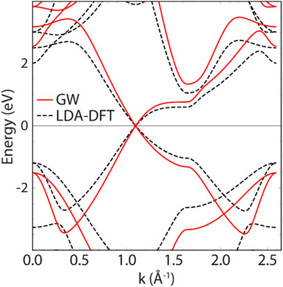
FIGURE 1. Band structure of freestanding silicene along the high symmetry
It is worth noting that the LDA results show a lowering of the bands, while the gaps at the Γ (3.3
We now focus on the region around the Dirac cone (K point) by examining energy-momentum data obtained from GW calculations of freestanding silicene. We have considered the first conduction (
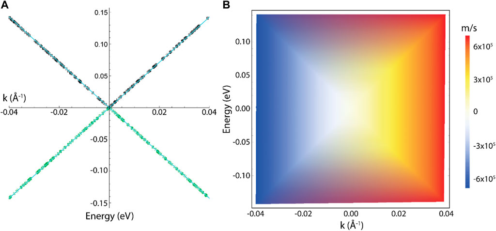
FIGURE 2. The low-energy band structure and charge-carrier velocity of freestanding silicene near the K point and around the Fermi level. (A) Displays the energy bands of silicene with the
Figure 2B displays the linear behavior of charge-carrier velocity, although only within a narrower energy range (
Specifically, Table 1 compares the estimated values by LDA-DFT (
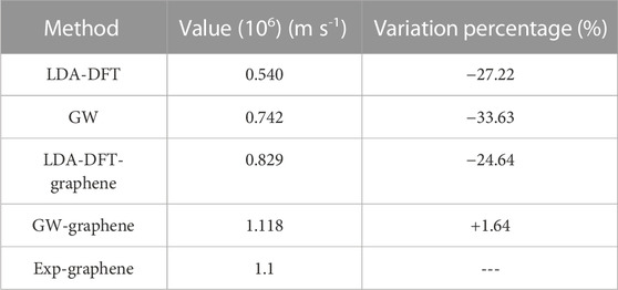
TABLE 1. The charge-carrier velocity of silicene is estimated by LDA and GW calculations. The results are compared with the experimental (Exp-graphene) [42] y theoretical (GW-graphene) values of graphene.
3.2 Electronic properties of SiNSs
Equation 11 demonstrates that there is an inverse relationship between the bandgap and ribbon width. Specifically, as the width of the ribbon increases, the bandgap value decreases exponentially. Therefore, if the ribbon width were to approach infinity (
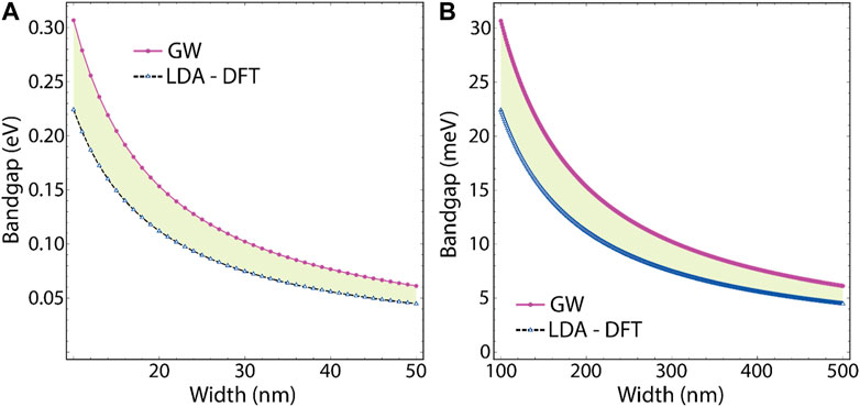
FIGURE 3. Comparison of the estimated bandgap values for SiNSs with widths ranging from (A) 10–50 nm and (B) 100–500 nm, using both GW (
The impact of ribbon width on the bandgap is most pronounced apparently in narrow SiNSs with widths ranging from 10 to 50 nm, as shown in Figure 3A, where the bandgap decreases from 0.3 eV to 50 meV. Conversely, wider SiNSs with widths ranging from 100 to 500 nm, shown in Figure 2B, exhibit a decrease in bandgap from 30 meV to 5 meV. In both cases, the bandgap decreases by a factor of six. Moving forward, we will focus on the electronic properties of SiNSs using the charge-carrier velocity of silicene obtained through GW calculations (i.e.,
Table 2 presents information on the bandgaps and effective electron masses for various nanostrips with different widths ranging from 100 to 500 nm. The data reveals a noteworthy trend: the wider the nanostrip, the smaller the bandgap. This trend is evident in the 100 nm wide nanostrip, which has a bandgap of approximately 30 meV, compared to the 500 nm wide nanostrip, which has a bandgap of approximately 6 meV. Furthermore, when comparing the same nanostrips, the effective electron masses show the same trend. The effective electron mass values obtained for the different nanostrips are consistent with both experimental findings and predictions for graphene nanostrips [43], [45], in terms of orders of magnitude. These results suggest that the properties of the SiNSs are similar to those of graphene nanostrips.
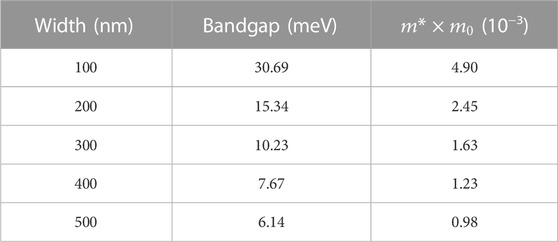
TABLE 2. Bandgap (meV) and effective mass (
In Figure 4, we now present the band structure (Figures 4A, C) and density of states (DOS) (Figures 4B, D) of the 100 nm and 500 nm wide nanostrips, in a
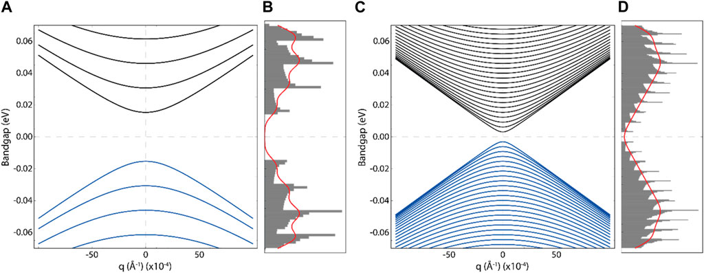
FIGURE 4. Band structure and density of states (DOS) of two SiNSs with different widths: (A, B) 100 nm and (C, D) 500 nm. The DOS is calculated from the energy-momentum data list using a conventional histogram with equal bin widths, and the red line represents the smoothed curve of the histogram.
Upon comparison, it becomes apparent that there is a quadratic band dispersion of the conduction and valence bands near the
Figures 4B, D show the DOS of the 100 nm and 500 nm wide nanostrips, respectively. These figures display several peaks corresponding to the bands in the band structure plot. Interestingly, smoothing the DOS histogram (red line) can lead to a narrower bandgap of the system. For example, the bandgap of the 100 nm wide nanostrip is roughly 23 meV, while that of the 500 nm wide nanostrip is around 4 meV. This results in a 23% and 33% reduction in the bandgap, respectively (Table 2).
3.3 Charge density effect
In this section, we investigate the plasmonic properties of SiNSs, focusing on the effect of charge carrier density (
Indeed, previous studies have reported that the charge carrier density in isolated graphene nanostrips is approximately
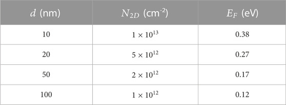
TABLE 3. 2D charge density and Fermi level shift, as influenced by different vacuum distances between adjacent nanostrips. The expression used to modulate the charge density is
Figure 5A shows the dispersion of plasmon frequency-momentum for a 100 nm wide nanostrip as a function of the reciprocal wave vector (
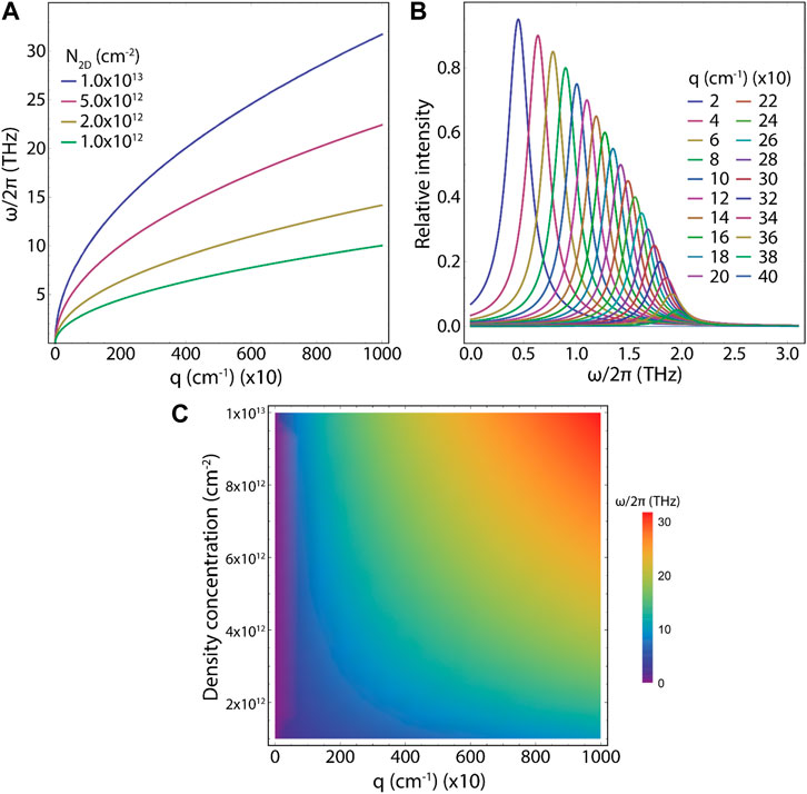
FIGURE 5. (A) Plasmon frequency dispersion by altering the vacuum distance between neighboring nanostrips. (B) The maximum of the plasmon peak for specific momentum values. (C) Density plot of the plasmon frequency-momentum dispersion as a function of density concentration and momentum. Results for a 100 nm wide nanostrip with:
Additionally, Table 3 indicates that a separation distance of 10 nm results in a high charge density (
Considering this, Figure 5B shows the dispersion of the maximum of the plasmon peak for a 100 nm wide nanostrip with a charge density of
3.4 Effective mass effect
The effective electron mass (
Eq. 10 contains this parameter, which is only affected by changes in the bandgap, such as those resulting from modifications to the ribbon width (Table 2) since the charge-carrier velocity (
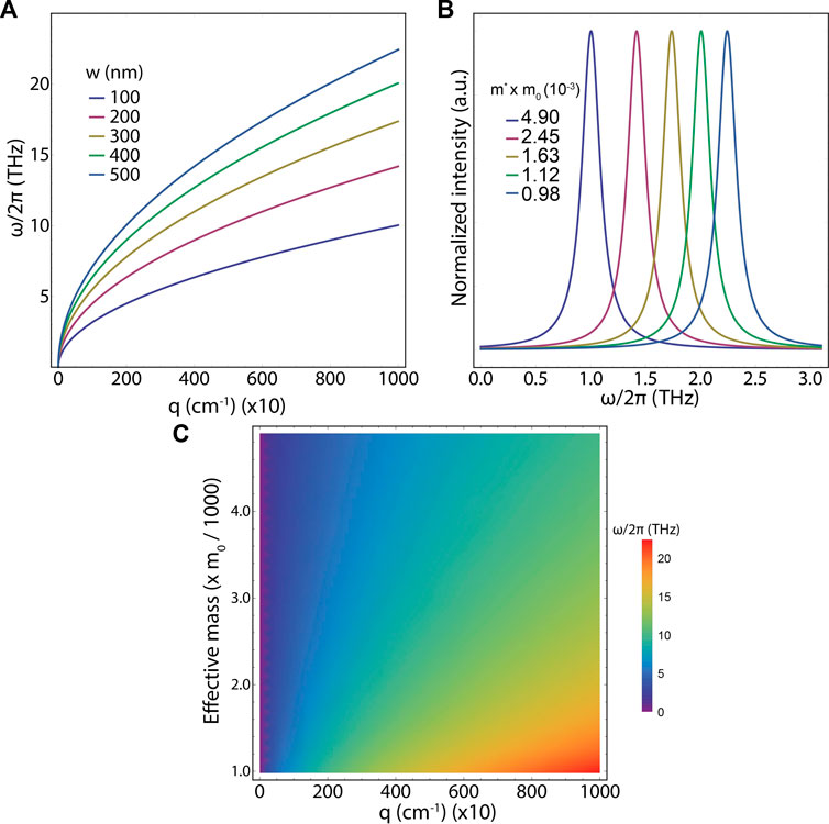
FIGURE 6. (A) Plasmon frequency dispersion by altering the effective electron mass which is modulated by increasing the ribbon width from 100 to 500 nm. (B) The maximum of the plasmon peak at
Figure 6B provides compelling evidence of the controllability and tunability of plasmon response, showing that increasing the width of the nanostrip or decreasing the effective electron mass results in an increase in plasmon frequency. This figure focuses on a frequency range of 0.1–3 THz, which is highly relevant for plasmonic applications in silicene, as mentioned earlier. Therefore, nanostrip systems ranging from 100 to 500 nm hold promise as potential candidates for such applications. Furthermore, Figure 6C demonstrates that there are no forbidden regions for plasmons and confirms that a decrease in the effective electron mass leads to an increase in plasmon frequency by approximately 25 THz (red region).
A final remark, Fei et al. [30] have successfully prepared graphene nanostrips with widths similar to those examined in this study (i.e.,
3.5 Excitation angle effect
The plasmon excitation angle (
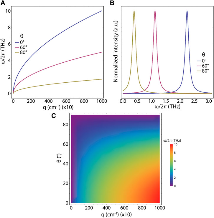
FIGURE 7. (A) Plasmon frequency dispersion by altering the plasmon excitation angle from
Figure 7C exhibits the existence of forbidden regions where plasmons are prohibited, and as the angle increases. Interestingly, these prohibited regions can also be observed by increasing the momentum value (as evidenced by the extended purple region). Moreover, it is important to highlight that the highest spectral intensity is achieved with small angles (
3.6 Electron relaxation effect
Electron relaxation rate (
Then, we focus on the electron relaxation rate in nanostrip of 100 and 500 nm wide. Additionally, this parameter is crucial in providing the values for electronic mobility and plasmon relaxation rate (Eq. 8) as shown in Table 4. Particularly, the electron mobility (
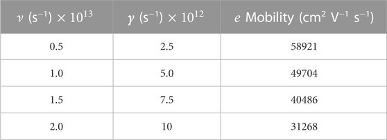
TABLE 4. The calculated values of electron relaxation rate (
Figure 8A depicts the plasmon frequency-momentum dispersion of a 100 nm wide nanostrip as a function of the increasing electron relaxation rate. Notably, the curves appear to overlap, prompting us to investigate whether this effect is attributable to the width of the strip. To that end, we analyzed a 500 nm wide nanostrip (as shown in Figure 8B) but found that the plasmon frequency-momentum dispersion followed the same pattern.
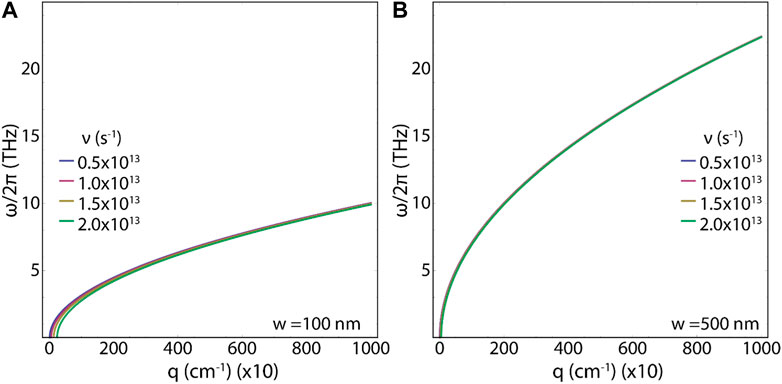
FIGURE 8. Plasmon frequency dispersion by altering the electron relaxation rate: Results for (A) 100 nm wide nanostrip and (B) 500 nm wide nanostrip (
Given that this effect is not due to strip width, we continue the analysis to a lower momentum regime for a 100 nm wide nanostrip, as depicted in Figure 9. We observe in Figure 9A that the plasmon frequency continues to be proportional to the square root of
(i) The plasmonic response moves towards higher momentum values.
(ii) The frequency of the plasmonic response drops significantly.
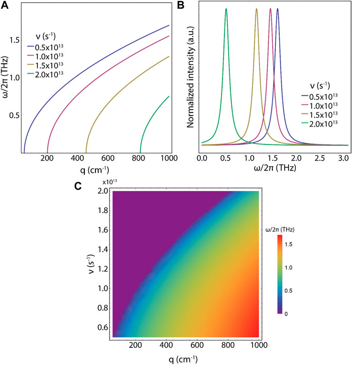
FIGURE 9. (A) Plasmon frequency dispersion by altering the electron relaxation rate. (B) The maximum of the plasmon peak at
Apart from the significant influence of the electron relaxation rate, Figure 9B shows that even a 100 nm wide SiNS subjected to the electron relaxation rate effect displays plasmon responses in the frequency range of 0.1–3 THz, suggesting even greater adjustable plasmonic properties. Figure 9C demonstrates the existence of forbidden regions for plasmons, which become more prominent as the electron relaxation rate and momentum increase (purple region). As previously mentioned, increasing the electron relaxation rate results in a significant reduction in the plasmon frequency. For instance, in a 100 nm wide nanostrip, the plasmon frequency reaches a maximum of around 2 THz (red region).
Hence, Eq. 4 provides a comprehensive understanding of the parameters that influence the plasmon response, including its frequency and dispersion. By thoroughly examining these parameters, one can manipulate them individually or in combination to customize the plasmon response for a specific application.
4 Conclusion
In summary, we have utilized a semi-analytical model that relies on the charge-carrier velocity of silicene as its main input parameter. To determine the charge-carrier velocity, we conducted LDA-DFT computations, resulting in
Our results indicate that SiNSs with widths ranging from 100 nm to 500 nm possess bandgap values in the range of a few meV. Specifically, we found that nanostrips with widths of 100, 200, 300, 400, and 500 nm exhibit bandgaps of approximately 30, 15, 10, 8, and 6 meV, respectively. Furthermore, the effective electron mass for these systems ranges from
Furthermore, our study provides a comprehensive investigation into the plasmonic properties of various nanostrips, including the effects of ribbon width, charge density, plasmon excitation angle, and electron relaxation rate. Particularly, we demonstrate that by adjusting these parameters individually or in combination, it is possible to achieve the desired plasmon resonance, enabling precise control and customization of plasmonic properties to meet specific application requirements. As the main findings, all the nanostrips examined in this study display a
Our study provides a thorough understanding of the electronic and plasmonic properties of SiNSs, which is essential for the advancement of future nanodevices. The insights gained from our research can serve as a valuable reference for future experiments aimed at verifying and building upon our findings.
Data availability statement
The raw data supporting the conclusion of this article will be made available by the authors, without undue reservation.
Author contributions
Conceptualization, TT and CVG; Methodology, MB, MJMS, and MLPR; Validation, TT, MG, and CVG; Formal Analysis, CG; Resources, TT; Data Curation, TT; Writing—Original Draft Preparation, CVG; Writing—Review and Editing, CVG. TT; Funding Acquisition, TT. All authors have read and agreed to the published version of the manuscript. All authors contributed to the article and approved the submitted version.
Funding
This work was funded by Universidad Técnica Particular de Loja (UTPL-Ecuador) under the project: “Análisis de las propiedades térmicas del grafeno y zeolita” Grand No: PROY_INV_QU_2022_362.
Acknowledgments
TT, MG, and CG wish to thank the Ecuadorian National Department of Sciences and Technology (SENESCYT). This work was partially supported by LNF-INFN: Progetto HPSWFOOD Regione Lazio—CUP I35F20000400005.
Conflict of interest
The authors declare that the research was conducted in the absence of any commercial or financial relationships that could be construed as a potential conflict of interest.
Publisher’s note
All claims expressed in this article are solely those of the authors and do not necessarily represent those of their affiliated organizations, or those of the publisher, the editors and the reviewers. Any product that may be evaluated in this article, or claim that may be made by its manufacturer, is not guaranteed or endorsed by the publisher.
Supplementary material
The Supplementary Material for this article can be found online at: https://www.frontiersin.org/articles/10.3389/fphy.2023.1198214/full#supplementary-material
References
1. Jose D, Datta A. Structures and chemical properties of silicene: Unlike graphene. Acc Chem Res (2014) 47(2):593–602. doi:10.1021/ar400180e
2. Molle A, Grazianetti C, Tao L, Taneja D, Alam MH, Akinwande D. Silicene, silicene derivatives, and their device applications. Chem Soc Rev (2018) 47(16):6370–87. doi:10.1039/c8cs00338f
3. Tokmachev AM, Averyanov DV, Parfenov OE, Taldenkov AN, Karateev IA, Sokolov IS, et al. Emerging two-dimensional ferromagnetism in silicene materials. Nat Commun (2018) 9(1):1672. doi:10.1038/s41467-018-04012-2
4. Chowdhury S, Jana D. A theoretical review on electronic, magnetic and optical properties of silicene. Rep Prog Phys (2016) 79(12):126501. doi:10.1088/0034-4885/79/12/126501
5. Drummond ND, Zolyomi V, Fal'Ko VI. Electrically tunable band gap in silicene. Phys Rev B (2012) 85(7):075423. doi:10.1103/physrevb.85.075423
6. Qin G, Qin Z, Yue SY, Yan QB, Hu M. External electric field driving the ultra-low thermal conductivity of silicene. Nanoscale (2017) 9(21):7227–34. doi:10.1039/c7nr01596h
7. Gao N, Zheng WT, Jiang Q. Density functional theory calculations for two-dimensional silicene with halogen functionalization. Phys Chem Chem Phys (2012) 14(1):257–61. doi:10.1039/c1cp22719j
8. Ni Z, Liu Q, Tang K, Zheng J, Zhou J, Qin R, et al. Tunable bandgap in silicene and germanene. Nano Lett (2012) 12(1):113–8. doi:10.1021/nl203065e
9. Fang D-Q, Zhang S-L, Hu X. Tuning the electronic and magnetic properties of zigzag silicene nanoribbons by edge hydrogenation and doping. Rsc Adv (2013) 3(46):24075–80. doi:10.1039/c3ra42720j
10. Sahoo S, Sinha A, Koshi NA, Lee SC, Bhattacharjee S, Muralidharan B. Silicene: An excellent material for flexible electronics. J Phys D: Appl Phys (2022) 55(42):425301. doi:10.1088/1361-6463/ac8080
11. Liang Y, Wang V, Mizuseki H, Kawazoe Y. Band gap engineering of silicene zigzag nanoribbons with perpendicular electric fields: A theoretical study. J Phys Condensed Matter (2012) 24(45):455302. doi:10.1088/0953-8984/24/45/455302
12. Sadegh MA, Calizo I. Band gap tuning of armchair silicene nanoribbons using periodic hexagonal holes. J Appl Phys (2015) 118(10):104304. doi:10.1063/1.4930139
13. Yang Y, Murali R. Impact of size effect on graphene nanoribbon transport. IEEE Electron Device Lett (2010) 31(3):237–9. doi:10.1109/led.2009.2039915
14. Niu T, Zhang J, Chen W. Atomic mechanism for the growth of wafer-scale single-crystal graphene: Theoretical perspective and scanning tunneling microscopy investigations. 2D Mater (2017) 4(4):042002. doi:10.1088/2053-1583/aa868f
15. Bhowmik S, Rajan AG. Chemical vapor deposition of 2D materials: A review of modeling, simulation, and machine learning studies. Iscience (2022) 25:103832. doi:10.1016/j.isci.2022.103832
16. Le Lay G, Aufray B, Léandri C, Oughaddou H, Biberian JP, De Padova P, et al. Physics and chemistry of silicene nano-ribbons. Appl Surf Sci (2009) 256(2):524–9. doi:10.1016/j.apsusc.2009.07.114
17. Yue N, Zhang Y. Growth and characterization of graphene, silicene, SiC, and the related nanostructures and heterostructures on silicon wafer. In: Modeling, characterization, and Production of nanomaterials. Sawston: Woodhead Publishing (2023). p. 337–361.
18. Chandiramouli R, Srivastava A, Nagarajan V. NO adsorption studies on silicene nanosheet: DFT investigation. Appl Surf Sci (2015) 351:662–72. doi:10.1016/j.apsusc.2015.05.166
19. Chegel R, Hasani M. Electronic and thermal properties of silicene nanoribbons: Third nearest neighbor tight binding approximation. Chem Phys Lett (2020) 761:138061. doi:10.1016/j.cplett.2020.138061
20. Pan L, Liu HJ, Tan XJ, Lv HY, Shi J, Tang XF, et al. Thermoelectric properties of armchair and zigzag silicene nanoribbons. Phys Chem Chem Phys (2012) 14(39):13588–13593. doi:10.1039/c2cp42645e
21. Popov VV, Bagaeva TY, Otsuji T, Ryzhii V. Oblique terahertz plasmons in graphene nanoribbon arrays. Phys Rev B (2010) 81(7):073404. doi:10.1103/physrevb.81.073404
22. Tene T, Guevara M, Viteri E, Maldonado A, Pisarra M, Sindona A, et al. Calibration of fermi velocity to explore the plasmonic character of graphene nanoribbon arrays by a semi-analytical model. Nanomaterials (2022) 12(12):2028. doi:10.3390/nano12122028
23. Gonze X, Amadon B, Antonius G, Arnardi F, Baguet L, Beuken JM, et al. The ABINIT project: Impact, environment and recent developments. Comput Phys Commun (2020) 248:107042. doi:10.1016/j.cpc.2019.107042
24. Perdew JP, Zunger A. Self-interaction correction to density-functional approximations for many-electron systems. Phys Rev B (1981) 23(10):5048–79. doi:10.1103/physrevb.23.5048
25. Gonze X, Amadon B, Anglade PM, Beuken JM, Bottin F, Boulanger P, et al. Abinit: First-principles approach to material and nanosystem properties. Comput Phys Commun (2009) 180(12):2582–615. doi:10.1016/j.cpc.2009.07.007
26. Troullier N, Martins JL. Efficient pseudopotentials for plane-wave calculations. II. Operators for fast iterative diagonalization. Phys Rev B (1991) 43(11):8861–9. doi:10.1103/physrevb.43.8861
27. Monkhorst HJ, Pack JD. Special points for Brillouin-zone integrations. Phys Rev B (1976) 13(12):5188–92. doi:10.1103/physrevb.13.5188
28. Aryasetiawan F, Gunnarsson O. The GW method. Rep Prog Phys (1998) 61(3):237–312. doi:10.1088/0034-4885/61/3/002
29. Trevisanutto PE, Giorgetti C, Reining L, Ladisa M, Olevano V. Ab initio G W many-body effects in graphene. Phys Rev Lett (2008) 101(22):226405. doi:10.1103/physrevlett.101.226405
30. Fei Z, Goldflam MD, Wu JS, Dai S, Wagner M, McLeod AS, et al. Edge and surface plasmons in graphene nanoribbons. Nano Lett (2015) 15(12):8271–6. doi:10.1021/acs.nanolett.5b03834
31. Gomez CV, Pisarra M, Gravina M, Sindona A. Tunable plasmons in regular planar arrays of graphene nanoribbons with armchair and zigzag-shaped edges. Beilstein J nanotechnology (2017) 8(1):172–82. doi:10.3762/bjnano.8.18
32. Gomez CV, Pisarra M, Gravina M, Pitarke J, Sindona A. Plasmon modes of graphene nanoribbons with periodic planar arrangements. Phys Rev Lett (2016) 117(11):116801. doi:10.1103/physrevlett.117.116801
33. Nikitin AY, Guinea F, García-Vidal FJ, Martín-Moreno L. Edge and waveguide terahertz surface plasmon modes in graphene microribbons. Phys Rev B (2011) 84(16):161407. doi:10.1103/physrevb.84.161407
34. Jia J, Takasaki A, Oka N, Shigesato Y. Experimental observation on the Fermi level shift in polycrystalline Al-doped ZnO films. J Appl Phys (2012) 112(1):013718. doi:10.1063/1.4733969
35. Shao G. Work function and electron affinity of semiconductors: Doping effect and complication due to fermi level pinning. Energ Environ Mater (2021) 4(3):273–6. doi:10.1002/eem2.12218
36. Falkovsky LA, Varlamov AA. Space-time dispersion of graphene conductivity. The Eur Phys J B (2007) 56:281–4. doi:10.1140/epjb/e2007-00142-3
37. Pisarra M, Sindona A, Riccardi P, M Silkin V, M Pitarke J. Acoustic plasmons in extrinsic free-standing graphene. New J Phys (2014) 16;083003. doi:10.1088/1367-2630/16/8/083003
38. Novoselov KS, Geim AK, Morozov SV, Jiang D, Zhang Y, Dubonos SV, et al. Electric field effect in atomically thin carbon films. science (2004) 306;666–9. doi:10.1126/science.1102896
39. Yang L, Park CH, Son YW, Cohen ML, Louie SG. Quasiparticle energies and band gaps in graphene nanoribbons. Phys Rev Lett (2007) 99(18):186801. doi:10.1103/physrevlett.99.186801
40. Blaber MG, Henry AI, Bingham JM, Schatz GC, Van Duyne RP. LSPR imaging of silver triangular nanoprisms: Correlating scattering with structure using electrodynamics for plasmon lifetime analysis. The J Phys Chem C (2012) 116(1):393–403. doi:10.1021/jp209466k
41. Egerton RF. Electron energy-loss spectroscopy in the TEM. Rep Prog Phys (2008) 72(1):016502. doi:10.1088/0034-4885/72/1/016502
42. Zhang Y, Tan YW, Stormer HL, Kim P. Experimental observation of the quantum Hall effect and Berry's phase in graphene. nature (2005) 438(201):201–4. doi:10.1038/nature04235
Keywords: silicene, silicene nanostrips, THz plasmons, electronic properties, group velocity
Citation: Tene T, Guevara M, Borja M, Mendoza Salazar MJ, Palacios Robalino MdL, Vacacela Gomez C and Bellucci S (2023) Modeling semiconducting silicene nanostrips: electronics and THz plasmons. Front. Phys. 11:1198214. doi: 10.3389/fphy.2023.1198214
Received: 31 March 2023; Accepted: 27 April 2023;
Published: 10 May 2023.
Edited by:
Li Li, Harbin Institute of Technology, ChinaReviewed by:
Mauludi Ariesto Pamungkas, University of Brawijaya, IndonesiaShengxuan Xia, Hunan University, China
Copyright © 2023 Tene, Guevara, Borja, Mendoza Salazar, Palacios Robalino, Vacacela Gomez and Bellucci. This is an open-access article distributed under the terms of the Creative Commons Attribution License (CC BY). The use, distribution or reproduction in other forums is permitted, provided the original author(s) and the copyright owner(s) are credited and that the original publication in this journal is cited, in accordance with accepted academic practice. No use, distribution or reproduction is permitted which does not comply with these terms.
*Correspondence: Cristian Vacacela Gomez, dmFjYWNlbGFAbG5mLmluZm4uaXQ=