 Swarupa Ojha1,2
 Anil Chamuah
 Sanjib Bhattacharya
- 1Department of Electrical Engineering, OmDayal Group of Institutions, Howrah, West Bengal, India
- 2Department of Electrical Engineering, Jadavpur University, Kolkata, West Bengal, India
- 3UGC-HRDC (Physics), University of North Bengal, Siliguri, West Bengal, India
The AC conductivity of chalcogenide semiconductors doped with Ag2S was extensively studied, not only for applications in devices but also for academic interests. X-ray diffraction studies reveal the presence of GeS, Ag2S, Se5.1S1.9, Se2.57S5.43, Ag2Se, S3Se5, Se4.7S3.3, and Ag8S nanocrystallites. The characteristic vibration that appeared in the range 500–600 cm−1 is due to the Ag–S bond, and the vibrations at 3,700 and 1600 cm−1 can be assigned as the bending and stretching vibrations of the O–H bond, which may be formed due to the adsorption of H2O molecules on the Ag2S surface. DC electrical conductivity can be increased by optical phonon frequency, which may be involved in the enhancement of structural vibrations. At low temperatures, the “density of states” increases from 3.337 × 10¹⁹ to 2.396 × 10²¹ eV−1 cm−3, and at high temperatures, it enhances from 3.417 × 1028 to 1.1356 × 1031 eV– 1 cm−3. The correlated barrier hopping model explores the maximum barrier height for composition, x = 0.1 as 0.0292 eV. The modified non-overlapping small polaron tunnelling model reveals the polaron transfer activation energy for x = 0.2 as 0.09110 eV. The independence of the electrical relaxation process of the system on temperature and its dependence on composition were exhibited by the scaling of the conductivity spectra.
1 Introduction
Chalcogenide glasses, which are non-oxide glasses, mainly consist of chalcogens, i.e., a group 16 elements (sulphur, selenium, or/and tellurium) of the periodic table, with some other opposite elements [1]. These glasses are amorphous materials and are semiconducting in nature. In the field of material science and nanotechnology, they have become an interesting area of research because of their attractive and exceptional properties, which can be attained only from the combined effects of the properties of the different constituent elements of the glasses [1–3].
Chalcogenide glassy systems are promising applicants in various technological applications, like switching memory, optoelectronics, photovoltaics, infrared transmission and detection, biosensors, chemical sensors, optical fibres, and many more [1–3]. Therefore, recent works on these systems have been very challenging for the research community. To explicate the structural, optical, and electrical properties of these systems, many researchers have conducted theoretical and experimental studies [4, 5]. For developing new chalcogenides by changing their properties, efforts have been made [4, 6] in order to enhance their different properties, like electrical, thermo-physical, and dielectric. Due to their amorphous semiconducting nature, these systems are technologically very important, and they became an academic need for further study [3, 7]. A multi-component system is prepared here using a low-cost melt-quenching route with various elements such as selenium (Se), germanium (Ge), and salt-like silver sulphide (Ag2S). Recent work on the novel multi-component chalcogenide glassy system [4] reveals its usage in semiconductors at different audio frequencies and temperatures, as well as laser components with different wavelengths. Mehta et al. [4] established the fact that such multi-component chalcogenide glassy system could be used to improve it for the application of optoelectronic materials.
Recent research on Se reveals that it is of significant interest for its usage in photocells, xerography, etc. [1, 2]. Chains of long polymers with ring fragments are its fundamental features, which may consist of a mixture of Se8 rings and Sen chains [8]. Incorporation of network modifiers or formers in it leads to the formation of complex geometrical structures [8]. In comparison to As-doped systems, the chalcogenide system based on Ge–Se is eco-friendly [8]. Glassy systems based on Ge–Sb–Se have been used in optochemical sensors [8]. The current–voltage characteristics of such systems have been explained using different models such as the Poole–Frenkel effect, hopping conducting effect, tunnelling conducting effect, and space charge-limited conduction effect [9, 10]. Many researchers have made efforts [9–12] to explore the temperature and frequency dependence of electrical conductivity in some chalcogenide systems. However, more research is required to explore conduction mechanisms in such systems. Researchers are also involved in exploring the microscopic mechanisms accountable for dielectric relaxation at different frequencies and temperatures, which is established as one of the most suitable and delicate methods of reviewing the glass structure [13]. Direct current (DC) conductivity models [14–16] and the frequency and temperature dependence of alternating current (AC) conductivity [17–20] are considered essential tools for exploring transport phenomena in the complicated chalcogenide semiconductor under study.
Se is an interesting chalcogen that possesses the reversible phase transformation property [21], which opens up the possibility of its usage in many device applications like rectifiers, switches, photocells, and memory devices; however, it also has some drawbacks including a short lifetime and low photosensitivity [21–24]. These drawbacks can be removed by doping Se with elements having more sensitivity, smaller ageing effects, and a higher crystallisation temperature [22]. The glass transition temperature of the system can be improved by adding Ge to Se, which improves corrosion resistance [24]. However, these glassy alloys are not thermally stable, leading to crystallisation. In this research work, the incorporation of a third element Ag2S in the Ge–Se system was attempted in order to improve the stability of the present glassy alloys.
The main objective of this work is to investigate the electrical properties of Ag2S-doped chalcogenide systems based on selenium–germanium (Ge–Se). To interpret DC conductivity at high and low temperatures, the Greaves model and Mott’s variable range hopping (VRH) model were used [14–16]. The correlated barrier hopping [17–19] model and modified non-overlapping small polaron tunnelling [20] model were used for interpreting the temperature and frequency dependence of AC conductivity. Electric modulus formalism was employed to investigate the dielectric relaxation of the present glassy samples. Scaling behaviour was adopted to explore its applicability to the time–temperature superposition principle.
2 Experimental
To prepare a chalcogenide system with the composition xAg2S–(1–x) (0.5Se–0.5Ge) with x = 0.1 and 0.2, high-purity reagent-grade chemicals Ag2S, Se, and Ge (Adrich 99.9%) were used. The melt-quenching method was used for this purpose. In this method, all the chemicals were weighted as per the specific fractions and mixed using a mortar. Then, the sealing of quartz ampoules was carried out under a vacuum of 10−4 Torr. These ampoules were then kept inside a furnace (a single-chamber muffle furnace with the highest ambient temperature of 1,400°C made by Jay Cruicible Company). The temperature of the furnace was set to increase at a rate of 3°C per minute to 250°C. The furnace was set at that temperature for 2 h, and then, its temperature was increased to 750°C. After another 2 h, the temperature was increased to 900°C. After 5 h, the ampoules were taken out of the furnace and dropped immediately in crushed ice for rapid cooling of the melted mixture to obtain the glassy samples. In the melt-quenching method, amorphous solids can be produced from the molten states of materials by quick cooling of the molten materials in order to evade the growth of crystals in the solids. In this method, weighting and then the mixing of high-purity constituent elements take place, followed by melting in sealed evacuated quartz ampoules. Sealing the mixture in quartz ampoules under a vacuum of 10−3–10−4 Torr lowers the likelihood of the reaction of these glasses with oxygen at higher temperatures. The polycrystalline nature of these samples was confirmed by the X-ray diffraction (XRD) study.
Structural characterisation of this system was also carried out using Fourier-transform infrared (FT-IR) spectroscopy analysis. Here, an FT-IR spectrometer (Perkin–Elmer) was used to record the FT-IR spectra in the transmittance mode of KBr matrices of the prepared samples in a powdered form in the wavelength range of 4000 cm−1 to 400 cm−1 at 25°C and humidity at 50%–60%. The transmitted radiations are detected by using the FT-IR spectrometer, which converts the radiations into a spectrum. This spectrum produces a molecular fingerprint of the sample by indicating the transmission and absorption of radiations by the molecules of the sample. Two different molecular structures cannot generate an identical infrared spectrum. For this reason, FT-IR has become a powerful technique for the structural characterisation of materials. A silver paste was coated on both sides of the samples in order to carry out electrical measurements. A Keithley high-precision electrometer (Model No. 6514) was used to conduct DC conductivity measurements of the samples at various temperatures, and a Hioki LCR Hi-Tester (Model No. 3532-50) was used for carrying out the AC electrical measurements in the frequency range 42 Hz–5 MHz. The range of temperature for carrying out the measurements is 333 K–463 K. The structural changes induced by the addition of Ag2S in the Ge–Se network are expected to increase the depolymerisation degree of double and single germanium–selenium–germanium (Ge–S–Ge) bridges [10]. However, Se is expected to form a chain structure [10]. Consequently, layered clusters based on the high-temperature crystal structure of α-germanium-sulphide (α-GeS2) were formed. In this environment, the average Ag–S bond length is expected to be 2.57 Å [10]. This discussion directly indicates that the silver ions in the present compositions are not mobile in nature. Apart from that, the electronic conductivity is measured at ambient temperature (303 K) using Wagner’s DC polarisation method [10] by constructing the following type of cell for the highest conducting composition of the as-prepared chalcogenide semiconductor compound (−)Ag/chalcogenide semiconductor as electrolyte/C (+), where C is graphite used as a blocking electrode and Ag is silver used as a non-blocking electrode. It shows maximum conductivity, which directly indicates that Ag ions do not take part in the conduction process of the present system.
3 Results and discussion
3.1 XRD
XRD patterns of all the prepared samples are illustrated in Figure 1A, in which different peaks are shown, indicating the occurrence of GeS (JCPDS No. 71-0306), Ag2S (JCPDS No. 03-0844), Se5.1S1.9 (JCPDS No. 78-0266), Se2.57S5.43 (JCPDS No. 73-2267), Ag2Se (JCPDS No. 71-2410), S3Se5 (JCPDS No. 71-1,118), Se4.7S3.3 (JCPDS No. 71-0248), and Ag8S (JCPDS No. 83-0674) nanocrystallites [25–27]. The occurrence of these crystallites in Figure 1A points towards the short-range order of constituent atoms. The polycrystalline behaviour of the system is directly indicated by the various peaks in Figure 1A. The Williamson–Hall (W–H) plot [28, 29] can be used to determine the crystallite size and lattice strain in the system.
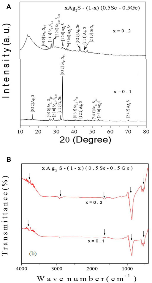
FIGURE 1. (A) X-Ray diffractograms and (B) FT-IR spectra of the chalcogenide xAg2S–(1–x) (0.5Se–0.5Ge) chalcogenide semiconductor with x = 0.1 and 0.2. Down arrow heads indicate various vibrational modes.
In this approximation, the broadening of peaks (βT), which arises due to the combined effects of micro-strain (βε) and crystallite sizes (βD), can be determined from the XRD data with the help of the following equation:
For calculating the crystallite size, the Scherrer equation (10) can be used, which is given by
Here, D is the crystallite size (in nm), λ = 0.15 nm (wavelength of the X-ray), βD (broadening of peak) is the measured full width at half maxima (FWHM) in radians [30], and θ is the peak position in radians.
In addition, the broadening of XRD peaks due to micro-strain [31, 32] can be represented as follows:
where ε is the developed micro-strain in the system.
Therefore, Eqs 1–3 reveal the following form:
Equation 4 can be used to compute the values of ε and D that are presented in Table 1.
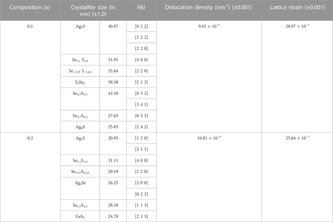
TABLE 1. Crystallite sizes along with various nanophases, dislocation density (nm−2), and lattice strain of the xAg2S–(1–x) (0.5Se–0.5Ge) glassy system for x = 0.1 and 0.2. Estimated errors are also included here.
Crystallographic defects or irregularities are developed due to the course of matrix formation in the form of dislocation. This is supposed to be highly responsible.
Due to the course of formation of matrices, crystallographic irregularities or defects are developed, which are supposed to be mainly responsible for the electrical transport via hopping of polarons. Dislocation density (δ) can be represented as follows:
The obtained values of δ are presented in Table 1.
The decrease in the average crystallite size with compositions can be observed in Table 1. With compositions, dislocation density is found to increase and micro-strain decreases. The increase in dislocations may be accountable for instigating the degree of altercations in structure and the grain boundary effect [33, 34].
So, the amalgamation of more Ag2S content in the system proposes to increase the dislocations and decrease the size of crystallites [33, 34]. High-order polaron conduction due to hopping may be induced by higher-order defects in the system [33, 34]. A more stable network structure is suggested by the steady decrease in the lattice strain (ε) values, which can be justified by the diffractograms of the system in Figure 1. The reduction in the size of nanocrystallites Ag2S, Se5.1S1.9, Se 2.57S 5.43, and Se4.7S3.3 and the disappearance of the phases S3Se5 and Se3.7S4.3 with the increase in x in the system were observed from XRD plot analysis. Configurations of crystallites, GeS and GeS2, are pronounced when the value of x is 0.2 in the system. It may be concluded from this discussion that on increasing Ag2S and decreasing Se and Ge in this system, a decrease in the crystallite size is found for all the phases in the system. This nature may indicate an inclination of sulphur to form a bond with Ge on increasing Ag2S content in the compositions. To instigate the structural altercations, which were previously mentioned, this result may be a possible reason.
The decrease in crystallite size with an increase in Ag2S content in the system can be clearly seen in Table 1. These data also indicate that the dislocation density, or the number of dislocation lines per unit volume, increases with the decrease in crystallite size. The change in dislocation density or defects in any system influences the electrical and mechanical properties of the system. The dislocations distort the structure of a system, which causes elastic stress around the distortion lines, which results in an increase in the strain in the system. So, with an increase in dislocation density, an increase in strain should have been found. However, here, it is found to be decreasing. The effects of grain boundaries may be a possible reason for these changes. As we can observe from Table 1 that the system x = 0.1 contains more grains (or phases) compared to the system x = 0.2, the higher value of strain in the system x = 0.1 may be due to the excessive volume of grain boundaries in the structure.
3.2 Study of FT-IR spectra
The FT-IR spectra of all samples are shown in Figure 1B. The characteristic vibration of Ag–S appears [35, 36] at 500–600 cm−1 in Figure 1B. 3,700 and 1,600 cm−1 in Figure 1B can be credited to the bending and stretching vibrations of the O–H bond due to the absorption of H2O molecules in the Ag2S surface [35, 36]. The vibrations at the lower and higher wave number zones (near 2920 cm−1 and 850 cm−1) in Figure 1B are expected to be responsible for asymmetric stretching modes of the bridges of the bonds Ge–Se and Ge–Se–Ge, respectively [35–37]. It is noteworthy that the vibration near 2920 cm−1 appears only for x = 0.2. The reason for this additional vibration may be due to the lesser amount of Ge and Se, which causes asymmetric stretching of the Ge–Se bond. Higher amounts of Ge and Se may be responsible for more and more asymmetric stretching vibrations of Ge–Se–Ge bonds near 850 cm−1.
It is possible to predict the optical phonon frequency (ν0) from the first absorption peak of IR vibration spectra [10, 35, 36]. This can be achieved by applying the relation C = λν0, where C is the average speed of light in vacuum and C = 3 × 10¹⁰ (cm/s), λ is the wavelength (cm), and ν0 is the optical phonon frequency (Hz). It may be a debatable issue as to the applicability of the first absorption peak of IF vibration spectra to determine the Debye temperature of the present amorphous semiconductor of a multi-component system. It is quite obvious that the optical phonon energy (ν0) may be responsible for Debye temperature, and the first absorption peak of IR vibration spectra provides optical phonon energy (ν0) [10, 35, 36].
The Debye temperature (θD) of the present chalcogenide semiconductor can be determined with the help of the following relation [10, 35, 36]:
where KB is the Boltzmann constant and h is Plank’s constant. In this analogy, it is quite appropriate to consider the optical phonon energy (ν0) of the first absorption peak of IR vibration spectra to estimate the Debye temperature, even if the system is a multi-component system. The computed values of optical phonon frequency and Debye temperature are presented in Table 2. It is clear from Table 2 that the values ν0 and θD are dependent on composition. ν0 is supposed to be the characteristic vibration of Ag–S. It can be seen from Table 2 that values of θD increase with the content of Ag2S. This indicates that the constituent atoms of the system exhibit higher kinetic energy, which may point towards higher electrical conductivity because of polaron hopping.
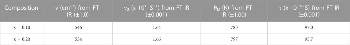
TABLE 2. Wavenumber (ν), optical phonon frequency (ν0), Debye temperature (θD), and relaxation time (τ) of the xAg2S–(1–x) (0.5Se–0.5Ge) chalcogenide semiconductor for x = 0.1 and 0.2. Estimated errors are also included here.
To estimate the relaxation time in the system, the relation τ = 1/(2πν0) can be used by approximating the transport of polarons as a part of the Debye-type relation [10, 11, 14]. The calculated relaxation time values are also presented in Table 2. A higher rate of polaron hopping is suggested because of the decrease in relaxation time with Ag2S [10, 14]. Higher electrical conductivity can be interpreted from this, which will be discussed afterwards.
3.3 DC conductivity
Figure 2A shows the variation of DC conductivity of this system with temperature, from which the thermally activated behaviour of the system can be observed. From Figure 2A, it can be observed that DC conductivity increases with an increase in temperature, and this indicates a non-linear nature, which suggests the semiconducting behaviour of the system. Figure 2B represents the dependency of DC conductivity on the compositions of the system at a fixed temperature. The increase in DC conductivity with an increase in the content of Ag2S in the composition is also notable.
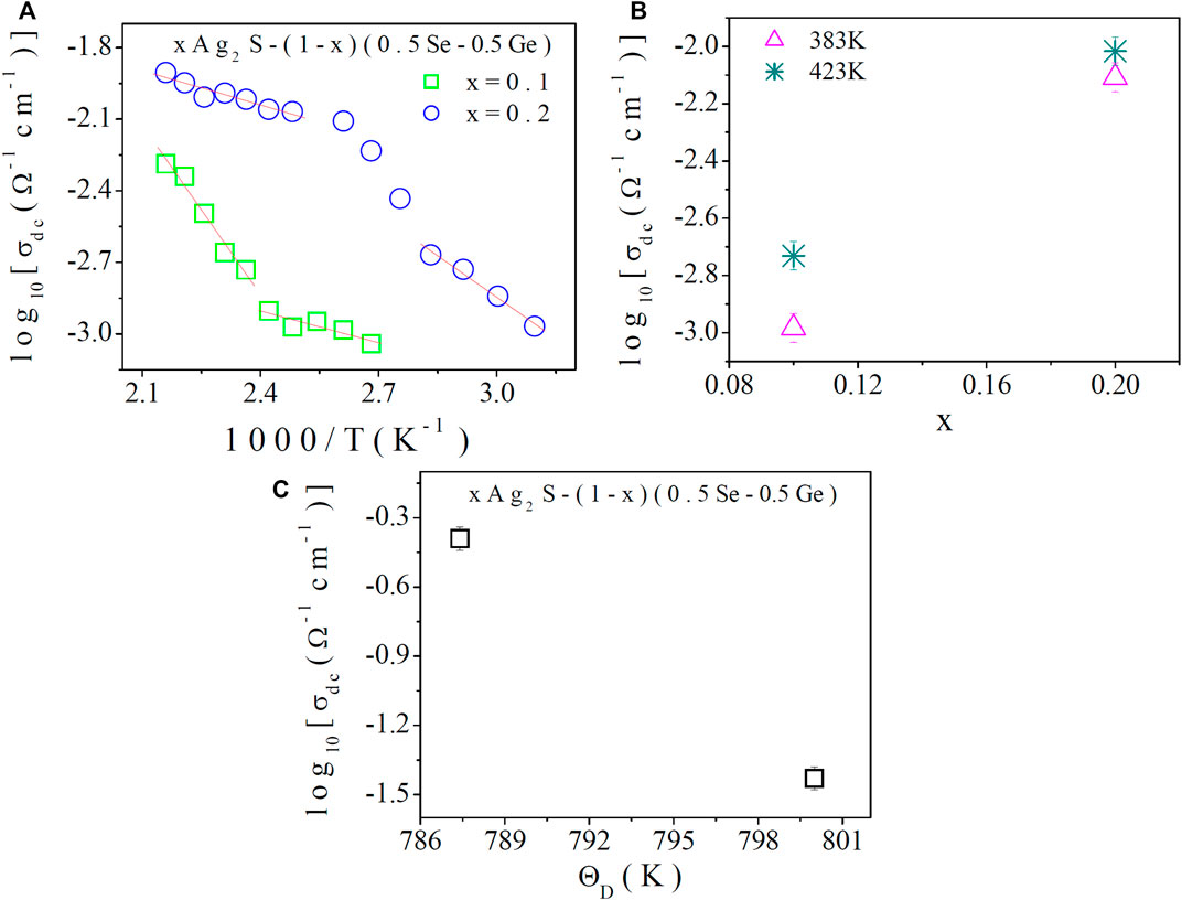
FIGURE 2. (A) Temperature dependence of DC electrical conductivity of chalcogenide semiconductor, xAg2S–(1–x) (0.5Se–0.5Ge), where x = 0.1 and 0.2; (B) fixed-temperature DC conductivity with compositions; and (C) DC conductivity (corresponding to the Debye temperature) versus Debye temperature of the present system.
Hence, it may be concluded that more polaron hopping may be instigated by the amalgamation of more Ag2S in the composition, which would result in enhanced DC conductivity in the system. From the slopes of the best-fitted straight lines in Figure 2A, low- and high-temperature activation energies were calculated, and they are presented in Table 3. Table 3 shows that the activation energy corresponding to DC conductivity in the high- and low-temperature regions is found to decrease with compositions. Schnakenberg [10, 14] described with good approximation the thermally activated DC conductivity data. In the polaron hopping model [10, 14], the high-temperature region is mainly associated with disordered energy (WD ≠0), and DC conductivity is primarily achieved by means of optical multi-phonon hopping. However, the main cause of DC conductivity at low temperatures is acoustical phonon-assisted hopping. With the increase in structural vibrations, the increase in DC conductivity of the system is confirmed by the FT-IR study and Table 3. It is also declared from the discussion that the low- and high-temperature DC activation energies (Eσ) are accountable for characterising the optical multi-phonon process of small polaron hopping among different localised states with the necessary condition, WD < Eσ.
TABLE 3. Estimated activation energy (Eσ) at lower- and higher-temperature regions corresponding to DC conductivity of the xAg2S–(1–x) (0.5Se–0.5Ge) chalcogenide semiconductor for x = 0.1 and 0.2. Estimated errors are also included here.
The DC conductivity corresponding to Debye temperature is projected in Figure 2C, which shows a gradual enhancement of DC conductivity. The increase in the transfer of phonon-assisted polaron energy is expected across grain boundaries because of the increase in the Debye temperature with more Ag2S doping in the system. Furthermore, defects and grain boundaries can soften phonons on the internal surfaces and contribute to the decrease in the Debye temperature [14]. The increase in dislocation density of the system is found (Table 1). In the present system, dislocation density (defects) is found to increase (Table 1) with more Ag2S content. A higher Debye temperature may be the reason for reducing the corresponding DC conductivity because, inside the structure, there is more phonon-assisted scattering. However, in Figure 2C, higher DC conductivity with Debye temperature can be observed. This result directly suggests the expansion of the present chalcogenide semiconductor due to the addition of Ag2S content to the structure, because of which the scattering cross section may be reduced as the dislocation density increases. As a result, DC conductivity increases.
Defects in localised states of this chalcogenide semiconductor can be made available [10, 11, 14–16] from the measurement data of DC conductivity. A variety of conduction mechanisms can be instigated in such systems owing to the density of defect states, N [EF], in the mobility gap, which may manage the conduction mechanisms in the semiconductor system [10, 11, 14–16].
Structural defects and impurities should affect the lower-temperature DC conductivity σdc, as suggested in Figure 2A. Mott’s VRH model [14, 15] can be used to predict the low-temperature conduction mechanism according to which carriers’ hopping takes place in localised states near the Fermi level.
As per this model [14, 15], the DC conductivity is expressed as follows:
where A and T0 are constants. T0 can also be represented as
where α−1 is the localisation length (α−1 = 10 Å).
DC conductivity data are presented in Figure 3A as a function of T−0.25. At a temperature below half the Debye temperature (θD/2) with α−1 = 10 Å [10, 11, 14–16], N (EF) values were measured from the slopes of the linear best-fit data in Figure 3A using Eq. 7. Table 4 shows the N (EF) values for different Ag2S content. It can be perceived from Table 4 that with the increase in the Ag2S content, because of grain boundary effects, N (EF) is found to increase in the lower-temperature regions [14].
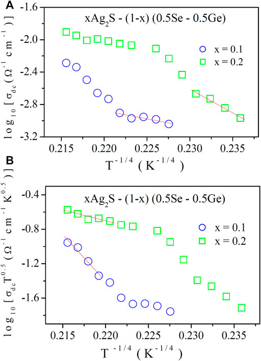
FIGURE 3. (A) Variations in DC conductivity at low temperatures as a function of T–0.25 (Mott’s model) and (B) Variation in σdc T1/2 as a function of T–0.25 (Greaves’s model). Solid lines are best-fitted linear fit data.
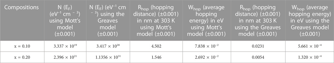
TABLE 4. The values of DOS near the Fermi level, hopping distance, and average hopping energy of the xAg2S–(1–x) (0.5Se–0.5Ge) chalcogenide semiconductor using Mott’s model and the Greaves model, respectively, for x = 0.10 and 0.20. Estimated errors are also included here.
In Figure 3B, high-temperature DC electrical conductivity is presented. The results indicate that the hopping of thermal-assisted tunnelling of charge carriers in extended states is responsible for the conduction [21]. DC conductivity data at higher temperatures [above half of the Debye temperature (θD/2)] were analysed using Greaves model [16]. As per this model, DC conductivity is represented as follows:
where A/ and T/0 are constants. T/0 is given by
At higher temperatures, values of N (EF) were obtained from the slopes of the linear best-fit data in Figure 5B using Eq. 9. Estimated N (EF) values are also shown in Table 4. It can be seen from Table 4 that N (EF) increases with the Ag2S content. The necessary course of strong couplings of phonons with quasi-local vibrations in the soft potential cores is suggested by high N (EF) [10–12].
This interaction may directly conceive a large number of localised states. Table 4 displays that N (EF) increases with compositions at higher temperatures, which may imply the formation of more localised states (defects) for polaron hopping. As we know from the XRD study that dislocation density increases with the Ag2S content in the compositions, further induction for the formation of more localised states in terms of the generation of more N (EF) values at higher temperatures is highly possible.
It is considerably noted from Table 4 that the N (EF) values found from Greaves model are much higher than those acquired from Mott’s model because they are functioning at different temperature ranges. As stated earlier, the present chalcogenide semiconductor is expanding, due to which the scattering cross section may get reduced, so N (EF) must be much higher at high temperatures.
It is established by many researchers [14–16, 19, 21] that the polaron binding energy becomes smaller than KBT and that the static disorder energy of the glassy system plays a vital role in the conduction processes at low temperatures (below the Debye temperature). In such a situation, Mott’s VRH model [14–16, 19, 21] is the most appropriate theoretical approximation to analyse DC conductivity data. Above 440 K, the linear portion of the DC conductivity data can be explained by variable range hopping due to Greave [14–16, 19, 21], which is similar to small polaron hopping via localised states. Attempts have been made by a group of researchers [14] to establish this conduction process. According to this proposition [14], microclusters in a glassy network play a pivotal role in DC conduction by multi-phonon tunnelling of polarons between microclusters.
For exploring the dependency of temperature on the conduction process, average hopping energy (Whop) and hopping distance (Rhop) can be considered as follows [14]:
and
The estimated values of Rhop and Whop at 303 K and 423 K are shown in Table 4 with the help of Mott’s and Greaves models, respectively. The essential requirements of the hopping models at any temperature are Rhop α ≥ 1 and Whop > KBT, which are satisfied unquestionably. From Table 4, it is clear that the addition of Ag2S causes a decrease in Rhop and Whop values. The smaller values of the hopping distance (Rhop) and hopping energy (Whop) make the conduction process in the system faster at higher temperatures because of the smaller time and energy requirements of the polaron for hopping among the nearest sites.
As a result, an increase in DC conductivity is found with compositions and temperatures.
3.4 Study of AC conductivity spectra
3.4.1 Analysis of experimental data using the power law, CBH model, and NSPT model
The thermally activated process of charge carriers may lead to the electrical conductivity of disordered solids in terms of hopping process under the influence of an electric field. Jonscher’s universal power law [38] is most suitable to analyse the AC conductivity data of amorphous semiconductors, which is
where σo is the conductivity at the low-frequency region (DC conductivity), which is found to be temperature dependent, S is the frequency exponent, and A is the pre-factor. The data on the AC conductivity of the system in the higher-frequency region were analysed. In Figure 4, the variation of AC conductivity of the system for x = 0.1 at various temperatures at high frequencies is illustrated, from which the linear increase in AC conductivity with frequency is found. Its increase with temperature can also be observed, which indicates its thermally activated mode. The data on AC conductivity in Figure 4 were fitted with least square straight lines using Eq. 13. The values of S were obtained from the slopes of these fittings. For exploring the nature of the conduction process in the present system, the variation of S with respect to temperature is shown in Figures 5A, B for x = 0.1 and 0.2, respectively. Remarkably, it is noted that S decreases with temperature for x = 0.1 and increases with temperature for x = 0.2, respectively. To gain essential insights into the conduction process, the experimental data in Figure 5A were subjected to analysis by fitting with appropriate theoretical models.
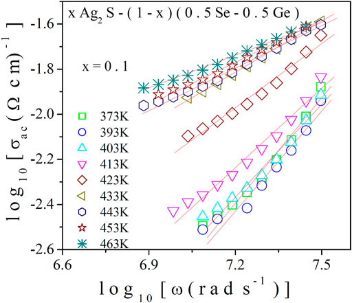
FIGURE 4. High-frequency conductivity spectra for x = 0.1. Solid lines indicate best-fitted straight lines, and slopes indicate “S”.
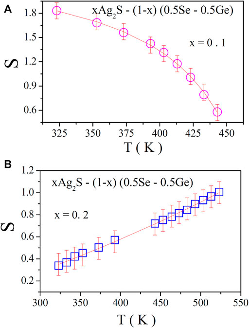
FIGURE 5. S–T plot of the chalcogenide xAg2S–(1–x) (0.5Se–0.5Ge) glassy system for (A) x = 0.1 and (B) x = 0.2. Solid lines (A) indicate the fitting of plots with the CBH model and (B) indicate the modified NSPT Model.
The nature of the temperature-dependent frequency exponent (S) can be used to find the origin of the conduction mechanism. The variation of S with temperature for the present system is found to decrease with the increase in temperature. To find out the major conduction mechanism of the AC conductivity of this system under study, we can propose a suitable model for the conduction mechanism in light of the different theoretical models correlating the conduction mechanism of the AC conductivity with S (T) behaviour. Here, the CBH model is found to be the most acceptable model to explore the feature of the conductivity mechanism in terms of describing the charge carrier hopping between two sites over a barrier separating them as the value of the frequency exponent (S) decreases with the increase in temperature [11, 14, 17–19]. The CBH model [11, 14, 17–19] has been widely applied to chalcogenide glassy semiconducting systems. As per the model, the conduction occurs via a bi-polaron hopping process in which two polarons simultaneously hop over the potential barrier between two charged defect states (D+ and D-), and the barrier height is correlated with the intersite separation via a Coulombic interaction. It is also noteworthy [11, 14, 17–19] that at higher temperatures, thermal excitation may be considered the possible reason for developing D+ and D- states (pair approximation) for single polaron hopping. Here, D+ and D- states are considered to be two localised states between which carriers (polarons) move back and forth with a particular relaxation time. In amorphous semiconductors (the present system), the localised states were considered to be randomly distributed in the space with such pairs of various relaxation times, which causes the present system to produce AC conductivity. On the other hand, the NSPT model [20] is used to interpret the conductivity mechanism when S is found to increase with temperature. Here, the nature of S with T compels us to think of the tunnelling of polarons [20] over the distance.
In search of such a model on a trial basis, the CBH model [11, 14, 17–19] was found appropriate for exploring the mechanism of conduction in this system. The CBH model [11, 14, 17–19] is applicable for systems with negative temperature dependence of S in which conduction takes place due to hopping of charge carriers in pairs between localised sites near the Fermi level. In the CBH model [10, 11], S is expressed as
where τ0 is the relaxation time and Wm is the maximum barrier height. The solid lines of Figure 5 specify the best-fitted curve using Eq. 14. The fitting parameters are given in Table 5.
TABLE 5. Different parameters obtained from the CBH and NSPT (modified) models of the xAg2S–(1–x) (0.5Se–0.5Ge) chalcogenide semiconductor for x = 0.1 and 0.2. Estimated errors are also included here.
In terms of AC conductivity, the CBH model [11, 14, 17–19] can be projected as follows:
where RHω is the hopping distance at frequency ω, N (EF) is the concentration of pair states, and n is the number of polarons involved in the hopping process. In this case, the bipolar hopping process may be expected to be the dominant conduction mechanism [10, 14]. The barrier height may be correlated with the inter-site separation via Coulombic interactions [10, 14]. Recent works by Karmakaretal [39, 40] clearly explained how the bipolar process may be expected to be the dominant conduction mechanism. For a single polaron hopping process [39, 40], the following relationship is considered:
where N is the carrier density of localised states, NP is the carrier hopping density of localised states, NT is the total density of states, and Ueff is the parameter in the dimension of energy.
The diminishing nature of Ueff with respect to frequency may ensure band-correlated polaronic conduction by the process of hopping in the considerable range of frequency and temperature. However, for the bipolar hopping process [39, 40], Ueff is considered to be zero, and consequently,
Here, Ueff is expected to play a significant role in making a correlation between the bipolar hopping process and the inter-site separation.
Attempts were made to investigate the data in Figure 5B, and consequently, the NSPT model [20] was used to fit the experimental data. Owing to the imperfect fitting of the NSPT model, it is slightly modified. This approximation of the NSPT model makes a perfect fit with the experimental data in Figure 5B. The modified NSPT model can be expressed as follows:
where τH is the relaxation time, WH is the activation energy for polaron transfer, and To is the temperature at which S becomes unity. The estimated values of WH, τH, and T (best-fitting parameters) are shown in Table 5. Using the modified NSPT model, the AC conductivity can be expressed as follows:
where e is the charge of an electron, ω is the angular frequency, N (EF) is the density of defect states at the Fermi level, R/Tω indicates the tunnelling distance at frequency ω, and α−1 is the localisation length of the wave function for small polarons. The modified NSPT fitting should suggest an approximation of the conduction process by means of tunnelling of polarons via the grain boundary for x = 0.2.
3.4.2 AC conductivity spectra
For exploring conduction pathways and the hopping frequency of charge carriers in the system, the AC conductivity spectra were analysed at different temperatures. The frequency-dependent AC conductivity σ(ω) in the low- and high-frequency window at diverse temperatures is shown in Figures 6A, B, respectively, for x = 0.2. The thermally activated nature of the conductivity spectra is obvious from Figure 6A. It is also observed that at low frequencies, a plateau region (which is frequency independent) occurs. This plateau region at low frequencies corresponds to DC conductivity, which increases with temperature. This nature suggests the thermally activated hopping of polarons [10, 41, 42]. However, dispersion in AC conductivity was observed at higher frequencies in Figure 6B, which may happen because of the correlated motion of polarons [10, 41, 42]. The spectra for AC conductivity of the system for other values of x showed similar nature. The frequency at which the dispersion in AC conductivity spectra starts is called the hopping or crossover frequency [10, 41–43]. The data on AC conductivity in the restricted zone in Figure 6B were analysed to get an insight into the conducting phenomena.
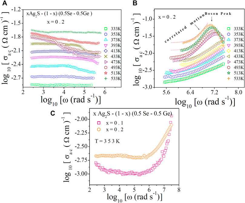
FIGURE 6. Conductivity spectra of the chalcogenidex Ag2S–(1–x) (0.5Se–0.5Ge) chalcogenide semiconductor for x = 0.2 at various temperatures in (A) low-frequency and (B) high-frequency zones, respectively. Position of the boson peak is mentioned by a down arrow head. (C) Conductivity spectra x = 0.1 and 0.2 at a fixed temperature.
In Figure 6B, high-frequency conductivity shows a peak, which apparently seems to be a boson peak (BP) [44]. In general, a boson peak [44] may arise in both ordered crystalline materials and disordered composite systems in the very high frequency (THz range) as an outcome of the competition between elastic mode propagation and diffusive damping. However, in the present system, it does exist in the MHz range. The peak maximum is found to change with temperature (T), but the frequency does not follow such a behaviour with T. Second, the BP peak in many chalcogenide semiconductors [10] always appears at THz frequencies. So, it may be concluded that the present peak in the MHz range may not be BP. The formation of some disorder states (oxygen bonding) in the compositions may be the possible reason for this peak in the MHz frequency range due to mutual interaction between the vibrational density of states and acoustic phonon damping [10]. Beyond the boson peak in Figure 6B, the conductivity spectra are found to fall down because of a loss in energy due to the abovementioned mutual interaction.
In Figure 6C, the conductivity spectra of the system at a particular temperature are shown. The increase in AC conductivity with temperature is observed in Figure 6A. This is in agreement with the plots of DC conductivity in Figure 2. In Figure 7A, the obtained values of ωH are plotted against temperature, from which thermally activated nature is proven. Hopping frequency at a fixed temperature (527 K) is shown in Figure 7B. Hopping frequency (ωH) (which is dependent on temperature) can be expressed with the help of the Arrhenius equation [10]as follows:
where ωα is the pre-exponential factor and EH is the activation energy for hopping frequency. The data in Figure 7A were best fitted using Eq. 20 to acquire the values EH. The obtained values of EH are shown in Table 5. An increase in EH is found with composition, though hopping frequency increases, which shows the similar nature of DC conductivity and the corresponding DC conductivity due to the grain boundary effects as discussed earlier.
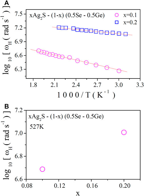
FIGURE 7. (A) Variation in the hopping frequency (ωH) with a reciprocal temperature; (B) variation in the hopping frequency (ωH) with x at a fixed temperature (527 K).
3.4.3 AC conductivity scaling
The electrical relaxation process can be interpreted from the time–temperature superposition principle [10, 43]. In this regard, the dependency of the conduction mechanism of a chalcogenide semiconductor on temperature and compositions can be explored by scaling AC conductivity data on a single master curve [10, 43]. In this consideration [10, 43], the axis of AC conductivity is scaled with respect to DC conductivity σdc, and the axis of frequency is scaled with respect to hopping frequency ωH. This process of scaling can be expressed as [10, 43]follows:
A universal scaling approach to conductivity with respect to composition was established by Ghosh and Pan [43]. According to their approach [43], in chalcogenide semiconductors, in the scaling process of conductivity spectra, the hopping frequency plays a very important role. The change in hopping lengths with composition in terms of the expression of the hopping frequency must instigate the connection between successive hops [43].
In Figure 8A, the AC conductivity scaling of this system with x = 0.2 at various temperatures is shown. From this figure, a perfect overlap of the conductivity spectra at different temperatures on a single master curve can be seen. The temperature-independent relaxation process can be indicated by this feature. For other compositions, an analogous feature was also observed. On the other hand, Figure 8B illustrates the scaling of AC conductivity for all samples of the system at a particular temperature. The non-overlapping of the conductivity spectra on a single master curve can be seen from the figure, which is an indication of the composition-dependent relaxation process. Hence, from the scaling of AC conductivity, it is observed that the relaxation dynamics nature of charge carriers (polarons) is composition dependent but temperature independent.
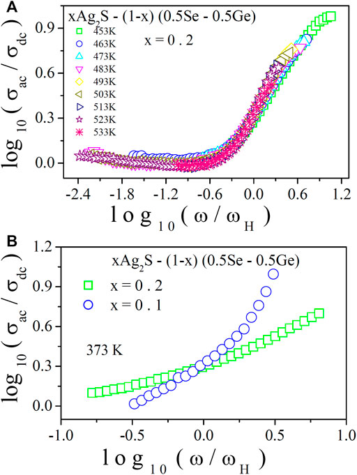
FIGURE 8. (A) Temperature scaling of conductivity spectra for x = 0.2 at various temperatures; (B) composition scaling of conductivity spectra at a fixed temperature (373 K).
The theoretical basis provides information [45] that local relaxation processes dominate at high frequencies and non-local processes at low frequencies. However, some deviations from prefect scaling in low-frequency regions (Figure 8A) are observed in the system under investigation. This observation suggests that some different and additional conductivity mechanisms may appear in the studied system. To explore local and non-local conduction mechanisms, experimental impedance data can be analysed in terms of equivalent circuit models of ideal resistors, capacitors, perhaps inductances, and possibly various distributed circuit elements [45]. Here, resistances in the high-frequency regime represent the bulk conductivity of the material [10, 45]. However, in the low-frequency regime, capacitances are generally associated with space charge polarisation regions and specific processes on an electrode [10, 45]. Non-local processes, such as the conduction of polarons, can be represented by the correlated motion of polarons [10, 45]. To gain further insights into the scaling process, it is observed that at lower temperatures, transport becomes non-local as tunnel effects start to play a role [45]. Polarisation effects and the non-diffusive nature of polaron conduction in low-frequency regimes may control local conduction in the scaling process [10, 45].
3.5 Dielectric properties
3.5.1 Electric modulus spectra and relaxation times
An obscurity in finding various dielectric parameters at low-frequency regions may be caused by the effects of electrode polarisation [10, 14, 20, 46, 47] on the dielectric spectra of the disordered system. To reduce the electrode polarisation effect, many researchers have put forth efforts in the past [10, 14]. To investigate the complex electrical response by invalidating the electrode polarisation effect, the electric modulus formalism [10, 14, 20, 46, 47] can be taken into account, which is equal to the reciprocal of complex permittivity.
The complex electrical modulus can be expressed as follows [10, 14, 20, 46, 47]:
where M* is the complex modulus, ɛ* is the complex dielectric permittivity, and M/ and M// represent the real and imaginary parts, respectively, of the electric modulus.
The assimilation of the electric modulus spectra over a wide frequency and temperature range forced us to explore the complete dielectric properties of the system. Figures 9A, B illustrate M/ and M// spectra, respectively, at various temperatures for x = 0.1. A similar nature was recorded for the other samples under study. It is noted in Figure 9A that at lower frequencies, M/ comes near zero due to the unavailability of the restoring forces of polarons [10, 11, 13, 14]. At higher frequencies, M/ shows dispersion and finally possesses the utmost value because of the electrical relaxation of polarons (charge carriers), which corresponds to (M∞) = (ε∞)−1 [11, 13, 14]. The peaks in the dielectric loss plots in Figure 9B play a very important role in estimating relaxation times. It can be seen from Figure 9A that M// approaches zero at lower frequencies, which indicates the repression of the electrode polarisation effect. In the high frequency region, the impact of the relaxation process makes M// maximum [10, 14, 20, 46, 47]. The decrease in M// is observed with the increase in frequency, which may indicate the short-range mobility of polarons in the system. In addition, the shifting of M// is observed in Figure 9A towards higher frequencies with an increase in temperature. This indicates that the relaxation process of this system is thermally activated. For other samples of the system, an analogous nature of electrical relaxation was observed. In Figure 9A, the M// peak positions correspond to the peak relaxation frequency (ωmax). In this approximation [10, 14, 20, 46, 47], ωmax indicates the limiting frequency up to which the charge carriers (polarons) may hop over long distances. Beyond the ωmax region, charge carriers are supposed to be confined to potential wells, where they are freely accessible [10, 11, 13, 14]. Hence, the transition of mobility of charge carriers from long-range to short-range orders takes place at ωmax.
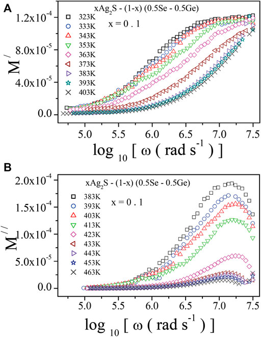
FIGURE 9. Frequency-dependent (A) real part of electric modulus, M/; (B) imaginary part of electric modus, M//, at various temperatures for x = 0.1.
For investigating M// nature, the following expression [10, 14, 20, 46, 47] can be applied:
where 0 < β < 1, M//max is the peak or maximum value of M//, ω max is the angular frequency corresponding to M//max, and β stands for the Kohlrausch–Williams–Watts (KWW) stretched coefficient [48, 49]. The experimental data in Figure 9B were analysed by best-fitted curves using Eq. 22. The values of M//max, ω max, and β were estimated from this fitting.
M// spectra of various as-prepared samples at a fixed temperature are presented in Figure 10A. It is evident from Figure 10A that M// is low for x = 0.2 as a large value of parallel capacitance was developed due to the contribution of the electrode polarisation effect [10, 11, 13, 14]. This result indicates the accumulation of a huge quantity of charge carriers for x = 0.2, which must be supported by higher conductivity data, as shown in Figure 2.
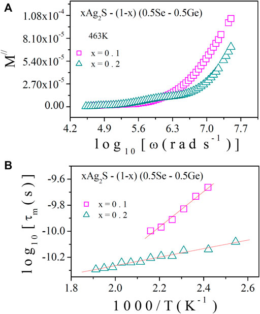
FIGURE 10. (A) M// spectra at a fixed temperature, T = 463 K; (B) relaxation time (τm) with reciprocal temperature.
For analysing the conduction mechanism of the system, it is approximated that the system undergoes relaxation of Debye type [24, 27], which involves the necessary condition: ωmax x τm = 1, where τm is the relaxation time. The calculated values of τm with reciprocal temperature are shown in Figure 10B. The thermally activated nature of τm is exhibited in Figure 10B. The decrease in τm is found with temperature change, which points to the semiconducting nature of the system. The decrease in τm with composition is validated by the nature of AC conductivity and hopping frequency, as shown in Figures 6, 7, respectively.
Figure 9A shows the real part of electric modulus M/, which is the reciprocal of the real part of permittivity ε/. From Figure 9, the increase in M/ values (i.e., decrease in the real part of permittivity) with the increase in frequency can be observed. At low frequencies, the alignment of dipoles is along the direction of the electric field. Therefore, due to electrode polarisation, which arises from space charge accumulation at glass-electrode interface, low values of M/ (i.e., high values of ε/) can occur at low-frequency region.
From Figures 9A, B, the decrease in both M/ and M// (i.e., an increase in ε/ and ε//) can be observed. This effect can be associated with the decrease in bond energies with the increase in temperature. The temperature rise weakens the intermolecular forces and enhances the orientational vibrations.
From Figure 9B, the shifting of peaks towards higher frequencies can be observed with the escalation of temperature. The occurrence of such shift is mainly due to the accumulation of free charges at the interface with the increase in temperature. Thus, relaxation time is decreased by the increase in the mobility of charge carriers. The shifting of peaks to higher frequencies with the increase in temperature is an indication of a thermally activated process in which charge carriers’ hopping mechanisms dominate intrinsically.
For studying thermally activated relaxation time in Figure 10B, the theoretical expression of relaxation time [10, 11, 13, 14] can be used in its form as follows:
where τ0 is the pre-exponential factor. Equation 24 was used to fit linearly the experimental data in Figure 10B. The slopes of the best-fitted straight lines helped in estimating the activation energy corresponding to relaxation time Eτ. The values of Eτ are shown in Table 6. The increase in Eτ is observed, indicating smaller values of relaxation times. The lower values of relaxation times and higher values of corresponding activation energy are signs of higher conductivity due to polaron hopping at a higher rate in the system. The short-term relaxation process may be considered to be insignificantly linked to the motion of the polaron. A thorough understanding of these relaxation processes may be connected to the lowest vibration of dipoles and conducting species at lower frequencies. To attain a relaxed state at higher frequencies, more activation energy is required by the dipoles because of their rapid vibrations. It is vital to state that relaxation times were calculated earlier using FT-IR spectra; the values are provided in Table 2. Those values were found to be much lower than those calculated from the dielectric relaxation process. The reason for such incongruity is that relaxation times calculated from the analysis of FT-IR utterly depend on vibrations due to optical phonon frequency (ν0) only. However, in the dielectric relaxation process, the results are supposed to be more precise because of the contributions of all types of lattice vibrations.
TABLE 6. Structural parameter (β) and activation energy corresponding to relaxation time (Eτ) of the xAg2S–(1–x) (0.5Se–0.5Ge) chalcogenide semiconductor for x = 0.1 and 0.2. Estimated errors are also included here.
Fitting of experimental M// data using Eq. 23 explores the KWW parameter (β) (Table 6), which should indicate the nature of relaxation [48, 49] in the present chalcogenide semiconductor. Extensive studies by Patel and Martin [50] revealed that ideal Debye-type single relaxation requires β→1. Their studies [50] also approximated β→0 for the maximum interaction among ionic systems. This discussion should suggest that moderate interactions may occur between polarons and lattices in the present chalcogenide semiconductor as β values are quite small.
3.5.2 Scaling of electric modulus
Efforts were made to scale electric modulus spectra at various temperatures [10, 11, 13, 14, 48, 49], similar to AC conductivity scaling. To obtain modulus scaling, values of M// (i.e., y-axis) were divided by M//max and ω (i.e., x-axis) values were divided by ωmax. One such scaling spectrum (for x = 0.2) is presented in Figure 11A. The analogous nature of temperature scaling was shown by all other samples of the system. The merging of all the scaled data in Figure 11A indicates that the relaxation process in the system is temperature independent [10, 11, 13, 14, 48, 49]. In Figure 11B, M// scaling spectra of all the samples of the system at 433 K are projected, in which non-merging of data is found. This is a sign of a composition-dependent relaxation process in the system. It is also notable that the nature of electric modulus scaling is similar to the behaviour of AC conductivity scaling. For exploring the conduction process in the system, the two methods (AC conductivity and electric modulus approaches) were used here independently. The results of these two different methods are similar interpretations of the experimental results.
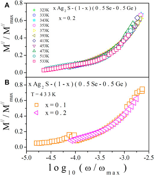
FIGURE 11. (A) Temperature scaling of M// at various temperatures for x = 0.2. (B) Composition scaling spectra of M// at 433 K
The data of conductivity of this complex semiconducting chalcogenide system can be described by considering a schematic model (Figure 12), which takes into consideration i) the free-carrier density in the system, ii) the internal potential barrier related to heterogeneity between crystallites and the surrounding amorphous phase, and iii) the amorphous phase. Based on these facts, a schematic model is proposed that consists of a) a cluster region, which represents a cluster of crystalline grains with the effective band gap (E1eV) of different nanocrystals, and b) a density of states (DOS) region, which consists of a simple DOS picture of an amorphous semiconductor with deep defects and tail states, having a mobility gap of E2eV. Between these two regions, a potential barrier is proposed to exist [51].
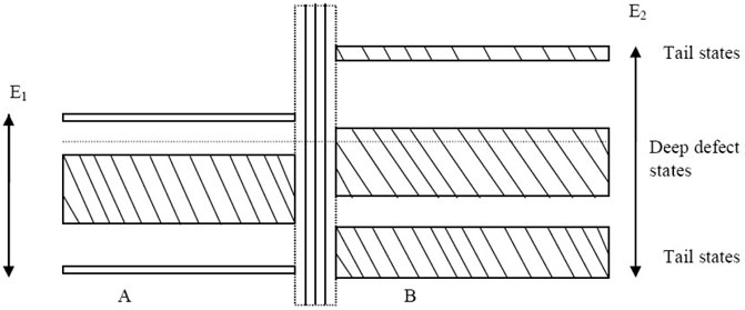
FIGURE 12. Proposed schematic model: (i) cluster region, representing a cluster of crystalline grains with the effective band gap of various nanocrystals (E1 eV); (ii) DOS region, consisting of a simple DOS picture of amorphous semiconductor with tail states and deep defects, having a mobility gap of E2 eV.
The enhancement of polaron density with a decrease in temperature at the boundary of amorphous and microcrystalline regimes has attracted a lot of attention due to its improved stability and transport properties [21]. On this type of material, high performance and stable films can be deposited [38, 41]. There are still a lot of unanswered questions related to the properties of the material at the transition region between the amorphous phases and the microcrystalline phases. The properties of this template material in a region of amorphous to microcrystalline transition are accompanied by a reduction in polaron density with temperature and a significant increase in the roughness of the surface [42].
4 Conclusion
AC conductivity and the dielectric relaxation process of Ag2S-doped new chalcogenide semiconductors were extensively studied over an extended range of frequencies and temperatures. The structural characterisation of the present system was carried out using XRD and FT-IR techniques. The size of the different nano-phases dispersed in the present chalcogenide matrices was estimated from the XRD study. Dislocation density and lattice strain were also computed from this study. FT-IR spectra indicated the presence of O–H and other functional groups in the system. Both the optical phonon frequency (ν0) and Debye temperature (θD) are found to be dependent on composition. For interpreting the AC conduction mechanism in the system, CBH and NSPT are found to be the most appropriate models for x = 0.1 and 0.2, respectively. The activation energy related to hopping frequency (EH) is found to decrease with Ag2S content. Activation energy associated with the relaxation process (Eτ) is found to increase with composition. The study of electric modulus formalism confirms the temperature dependence of the relaxation process. The temperature and composition scaling of both AC conductivity and M// spectra specifies that the relaxation process is contingent on composition but independent of the temperature of this system. A schematic model is proposed to shed some light on the polaron hopping process of this system. The present study deals with the study of frequency and temperature dependency in the electrical transport of xAg2S–(1–x) (0.5Se–0.5Ge), with x = 0.1 and 0.2, chalcogenide semiconductors. However, the identification of some possible solid-state device applications of these semiconducting glass nanocomposites for industry and academic purposes is yet to be determined. In addition, further structural characterisation of these materials using FE-SEM, DSC, etc., is to be carried out. To check the suitability of this material in various optical device applications, the study of optical properties is very significant.
Data availability statement
The original contributions presented in the study are included in the article/Supplementary Material; further inquiries can be directed to the corresponding author.
Author contributions
SB: conceptualization, methodology, writing—reviewing and editing, and supervision. SO: data curation, validation, and grammar check. MR: supervision. AC: software. All authors contributed to the article and approved the submitted version.
Funding
DST-CRG (Department of Science and Technology, Govt. of India) financially assisted this work (Sanction No. CRG/2018/000464).
Acknowledgments
AC is thankful to the Department of Science and Technology, Govt. of India, for providing research fellowship. SB (PI) also acknowledges the “Sophisticated Analytical Instrument Facility (SAIF)”of Gauhati University, Guwahati 781014, for providing XRD facility.
Conflict of interest
The authors declare that the research was conducted in the absence of any commercial or financial relationships that could be construed as a potential conflict of interest.
Publisher’s note
All claims expressed in this article are solely those of the authors and do not necessarily represent those of their affiliated organizations, or those of the publisher, the editors, and the reviewers. Any product that may be evaluated in this article, or claim that may be made by its manufacturer, is not guaranteed or endorsed by the publisher.
References
1. Eggleton BJ, Luther–Davis B, Richardson K. Chalcogenide photonics. Nat Photon (2011) 5:141–8. doi:10.1038/nphoton.2011.309
2. Hlavac J. The Technology of glasses and ceramics. Amsterdam, The Netherlands: Elsevier Scientific publishing company (1983). p. 220.
3. Tammam AK, Kahlifa Z, Elsayed SA. First and second phase transition discovery in amorphous chalcogenide Se60Te30S10 composition. J Non-crystalline Sol (2020) 529:119729. doi:10.1016/j.jnoncrysol.2019.119729
4. Stehlik S, Zima V, Wagner T, Ren J, Frumar M. Conductivity and permittivity study on silver and silver halide doped GeS2–Ga2S3 glassy system. Sol State Ionics (2008) 179:18671875. doi:10.1016/j.ssi.2008.05.001
5. Zalkovskij M, Strikwerda AC, Iwaszczuk K, Popescu A, Savastru D, Malureanu R, et al. Terahertz-induced Kerr effect in amorphous chalcogenide glasses. Appl Phys Lett (2013) 103:221102. doi:10.1063/1.4832825
6. Srivastava A, Chandel N, Mehta N. Novel explanation for thermal analysis of glass transition. Mat Sci Eng B (2019) 247:114378. doi:10.1016/j.mseb.2019.114378
7. Shen W, Baccaro S, Cemmi A, Ren J, Zhang Z, Zhou Y, et al. Gamma-ray irradiation resistance of silver doped GeS2–Ga2S3–AgI chalcohalide glasses. Nucl.Inst Meth.Phys Res B (2014) 329:48–51. doi:10.1016/j.nimb.2014.02.119
8. Seddon AB. Chalcogenide glasses: A review of their preparation, properties and applications. J Non-crystalline Sol (1995) 184:44–50. doi:10.1016/0022-3093(94)00686-5
9. Singh P, Sharma S, Tripathi S, Dwivedi D. Study of dielectric relaxation and thermally activated a.c. conduction in multicomponent Ge10−xSe60Te30Inx (0 ≤ x ≤ 6) chalcogenide glasses using CBH model. Results Phys (2019) 12:223–36. doi:10.1016/j.rinp.2018.11.048
10. Karmakar AB, RademannAndrey K, andStepanov L. Glass nanocomposites, synthesis, properties and applications. Amsterdam, Netherlands: Elsevier Inc (2016).
11. Majeed Khan MA, Kumar S, Husain M, Zulfequar M. Thermal properties of Selenium- Bismuth glassy alloys. Chalcogenide Lett (2007) 4:147.
12. Palui A, Ghosh A. Structure-transport correlation of super-ionic mixed network former glasses. Solid State Ionics (2019) 343:115126. doi:10.1016/j.ssi.2019.115126
13. Bhattacharya S, Ghosh A. Relaxation dynamics in superionic glass nanocomposites. J Am Cer Soc (2008) 91:753–9. doi:10.1111/j.1551-2916.2007.02099.x
14. Mott NF, Davis EA. Electronic processes in non-crystalline materials. Oxford): Clarendon Press (1979).
15. Mott NF. Conduction in non-crystalline materials: III. Localized states in a pseudogap and near extremities of conduction and valence bands. Mag (1969) 19:835–52. doi:10.1080/14786436908216338
16. Greaves GN. Small polaron conduction in V2O5P2O5 glasses. J Non-cryst Sol (1973) 11:427–46. doi:10.1016/0022-3093(73)90089-6
17. Mott NF. Conduction in glasses containing transition metal ions☆. J Non-cryst Sol (1968) 1(1):1–17. doi:10.1016/0022-3093(68)90002-1
18. Murugaraj R. Ac conductivity and its scaling behavior in borate and bismuthate glasses. J Mater Sci (2007) 42:10065–73. doi:10.1007/s10853-007-2052-5
19. Ghosh A. Transport properties of vanadium germanate glassy semiconductors. Phys Rev B (1990) 42:5665–76. doi:10.1103/physrevb.42.5665
20. Karmakar S, Behera D. Non-overlapping small polaron tunneling conduction coupled dielectric relaxation in weak ferromagnetic NiAl2O4. J Phys Condensed Matter (2019) 31:245701. doi:10.1088/1361-648x/ab03f0
21. Khan SA, Zulfequar M, Husain M. On the crystallization kinetics of amorphous Se80In20−xPbx. Solid State Commun (2002) 123:463–8. doi:10.1016/s0038-1098(02)00147-3
22. Suri N, Bindra KS, Kumar P, Thangaraj R. Calorimetric studies of Se80−xTe20Bix bulk samples. J Non Cryst Sol (2007) 353:1264–7. doi:10.1016/j.jnoncrysol.2006.10.056
23. Mathur R, Kumar A. Photoconductivity in amorphous thin films of Ge22Se68Bi 10. Rev Phys Appl (1986) 21:579–84. doi:10.1051/rphysap:019860021010057900
24. Chiba R, Funakoshi N. Crystallization of vacuum deposited TeSe Cu alloy film. J Non Cryst Sol (1988) 105:149–54. doi:10.1016/0022-3093(88)90349-3
25. Laitinen R, Niinistoe L, Steudel R. Structural studies on the sulfur-selenium binary system. Acta Chem Scand Ser.A (1979) 33:737–47. doi:10.3891/acta.chem.scand.33a-0737
26. Wiegers GA. The crystal structure of the low-temperature form of silver selenide. Am Mineral (1971) 56:1882.
27. Weiss JZ. Mitteilung über interchalkogenverbindungen, IV. Röntgenographische untersuchungen an mischkristallen der susammensetzung SenS8-n, Z. Anorg Allg Chem (1977) 435:113. doi:10.1002/zaac.19774350115
28. Nath D, Singh F, Das R. X-ray diffraction analysis by Williamson-Hall, Halder-Wagner and size-strain plot methods of CdSe nanoparticles-a comparative study. Mater.Chem Phys (2020) 239:122021. doi:10.1016/j.matchemphys.2019.122021
29. Mustapha S. Comparative study of crystallite size using Williamson-Hall and Debye-Scherrer plots for ZnO nanoparticles. Adv Nat Sci Nanosci Nanotechno (2019) 10:045013. doi:10.1088/2043-6254/ab52f7
30. Demichelis F, Crovini G, Osenga C, Pirri CF, Tresso E, Boarino L. Crystallinity and optoelectronic properties of μc-SiC:H. Mater.Res.Soc Symp.Proc (1993) 283:477. doi:10.1557/proc-283-477
31. Sheng S, Liao X, Kong G. Gap states of hydrogenated amorphous silicon near and above the threshold of microcrystallinity with subtle boron compensation. Appl Phys Lett (2001) 78:2509–11. doi:10.1063/1.1368185
32. Tsu DV, Chao BS, Ovshinsky SR, Guha S, Yang J. Effect of hydrogen dilution on the structure of amorphous silicon alloys. Appl Phys Lett (1997) 71:1317. doi:10.1063/1.119928
33. Janosi A. La structure du sulfure cuivreux quadratique. ActaCrystallogr (1964) 17:311–2. doi:10.1107/s0365110x64000743
34. Mittemeijer EJ, Fastenau RHJ, Van Ingen RP. Laser ablation deposition of Cu-Ni and Ag-Ni films: Nonconservation of alloy composition and film microstructure. J Appl Phys (1994) 76:1871–83. doi:10.1063/1.357711
35. Kim YY, Walsh D. Metal sulfidenanoparticles synthesized via enzyme treatment of biopolymer stabilized nanosuspensions. Nanoscale (2010) 2:240–7. doi:10.1039/b9nr00194h
36. Wu D, Jiang Y, Yuan Y, Wu J, Jiang K. ZnO–ZnS heterostructures with enhanced optical and photocatalytic properties. J Nanoparticle Res (2011) 13:2875–86. doi:10.1007/s11051-010-0176-z
37. Aly KA, Afify N, Saddeek YB, Abousehly AM. Elastic and optical properties of Ge x Se2Sb1−x (0.0 ≤ x ≤ 1.0) glasses. Bull Mater.Sci (2016) 39:491–8. doi:10.1007/s12034-016-1152-8
39. Karmakar S, Behera D. Band-correlated barrier-hopping conduction in α-NiMoO4 micro-crystals and comparison of its energy storage performance with MWCNT-integrated complex. J Mater Sci Mater Electron (2020) 31:5336–52. doi:10.1007/s10854-020-03094-3
40. Karmakar S, Behera D. High-temperature impedance and alternating current conduction mechanism of Ni0.5Zn0.5WO4 micro-crystal for electrical energy storage application. J Aust Ceram Soc (2020) 56:1253–9. doi:10.1007/s41779-020-00475-z
41. Almond DP, Duncan GK, West AR. The determination of hopping rates and carrier concentrations in ionic conductors by a new analysis of ac conductivity. Solid State Ionics (1983) 8:159–64. doi:10.1016/0167-2738(83)90079-6
42. Roling B, Happe A, Funke F, Ingram MD. Carrier concentrations and relaxation spectroscopy: New information from scaling properties of conductivity spectra in ionically conducting glasses. Phy Rev Lett (1997) 78:2160–3. doi:10.1103/physrevlett.78.2160
43. Ghosh A, Pan A. Scaling of the conductivity spectra in ionic glasses: Dependence on the structure. Phy Rev Lett (2000) 84:2188–90. doi:10.1103/physrevlett.84.2188
44. Baggioli M, Zaccone A. Universal origin of Boson peak vibrational anomalies in ordered crystals and in amorphous materials. Phy Rev Lett (2019) 122:145501. doi:10.1103/physrevlett.122.145501
45. El-Nahass MM, Ali HAM. AC conductivity and dielectric behavior of bulk Furfurylidenemalononitrile. Solid State Commun (2012) 152:1084–8. doi:10.1016/j.ssc.2012.03.002
46. Karmakar S, Parey V, Mistari CD, Thapa R, More MA, Behera D. Electric field emission and anomalies of electrical conductivity above room temperature in heterogeneous NiO-SnO2 nano-ceramic composites. J Appl Phys (2020) 127:034102.
47. Karmakar S, Tyagi H, Mohapatra DP, Behera D. Dielectric relaxation behavior and overlapping large polaron tunneling conduction mechanism in NiO–PbO μ-cauliflower composites. J Alloys Compd (2021) 851:156789. doi:10.1016/j.jallcom.2020.156789
48. Macedo PB, Moynihan CT, Bose R. The role of ionic diffusion in polarisation in vitreous ionic conductors. Phys Chem Glasses (1972) 13:171.
49. Macdonald JR, Kenan WR. Impedance spectroscopy: emphasizing solid materials and systems. New York: Wiley (1987).
50. Patel HK, Martin SW. Fast ionic conduction in Na 2 S+ B 2 S 3 glasses: Compositional contributions to nonexponentiality in conductivity relaxation in the extreme low-alkali-metal limit. Phys Rev B (1991) 45:10292.
Keywords: Ag2S-doped chalcogenide glassy system and microstructure, conductivity spectra and Boson peak, Mott’s and Greave’s models, correlated barrier hopping and non-overlapping small polaron tunnelling models, rrelaxation time and electric modulus
Citation: Ojha S, Chamuah A, Roy M and Bhattacharya S (2023) Comprehensive studies on the electrical transport of some chalcogenide semiconductors: frequency- and temperature-dependent AC conductivity. Front. Phys. 11:1151841. doi: 10.3389/fphy.2023.1151841
Received: 26 January 2023; Accepted: 17 July 2023;
Published: 04 August 2023.
Edited by:
James Avery Sauls, Louisiana State University, United StatesReviewed by:
Hamze Mousavi, Razi University, IranJianbao Zhao, Canadian Light Source, Canada
Masoud Salavati-Niasari, University of Kashan, Iran
Copyright © 2023 Ojha, Chamuah, Roy and Bhattacharya. This is an open-access article distributed under the terms of the Creative Commons Attribution License (CC BY). The use, distribution or reproduction in other forums is permitted, provided the original author(s) and the copyright owner(s) are credited and that the original publication in this journal is cited, in accordance with accepted academic practice. No use, distribution or reproduction is permitted which does not comply with these terms.
*Correspondence: Sanjib Bhattacharya, c2FuamliX3NzcEB5YWhvby5jby5pbg==, ZGRpcmhyZGNAbmJ1LmFjLmlu