
95% of researchers rate our articles as excellent or good
Learn more about the work of our research integrity team to safeguard the quality of each article we publish.
Find out more
ORIGINAL RESEARCH article
Front. Phys. , 30 March 2023
Sec. Condensed Matter Physics
Volume 11 - 2023 | https://doi.org/10.3389/fphy.2023.1149608
This article is part of the Research Topic Usage of Patterned Surfaces Formed Using Low-Energy Ions for Various Applications View all 4 articles
In recent decades, nanostructuring has become one of the most important techniques to design and engineer functional materials. The properties of nanostructured materials are influenced by the interplay of its instrinsic bulk properties and the properties of its surface - the relative importance of the latter being enhanced by the increased surface-to-volume ratio in nanostructures. For instance, nanostructuring of a thermoelectric material can reduce the thermal conductivity while maintaining constant electrical conductivity and the Seebeck coefficient, which would improve the thermoelectric properties. For that reason, this study investigated the possibility of preparing nanowires of iron antimonide (FeSb2), a thermoelectric material, on single-crystalline gallium arsenide GaAs (001) substrates with ion-induced surface nanoscale pre-patterning and characterized the structure of the prepared FeSb2 nanowires. The GaAs (001) substrates were pre-patterned using 1 keV Ar+ ion irradiation. By using an ion source with a broad, unfocused ion beam at normal incidence, the patterned area can be scaled to nearly any size. The self-organized surface morphology is formed by reverse epitaxy and is characterized by almost perfectly parallel-aligned ripples at the nanometer scale. For the fabrication of FeSb2 nanowires, iron and antimony were successively deposited on the pre-patterned GaAs substrates at grazing incidence and then annealed. They were characterized using transmission electron microscopy (TEM), in particular high-resolution TEM imaging for structure analysis and spectrum imaging analysis based on energy-dispersive X-ray spectroscopy for element characterization. With the presented fabrication method, FeSb2 nanowires were produced successfully on GaAs(001) substrates with an ion-induced nanopatterned surface. The nanowires have a polycristalline structure and a cross-sectional area which is scalable up to 22 × 22 nm2. Due to the high order nanostructures on the GaAs substrate, the nanowires have a length of several micrometer. This bottom-up nanofabrication process based on ion-induced patterning can be a viable alternative to top-down procedures regarding to efficiency and costs.
Ion irradiation offers a great possibility to modify the surface morphology of materials. Exposed to a broad ion beam, the surface of a solid is either smoothed or various nanoscale patterns emerge depending on the irradiation conditions and the material properties [1]. Ion irradiation induces erosive, redistributive, and diffusive processes on the material surface. As a result of these concurrent processes, hexagonally ordered dot or pit patterns [2], checkerboard patterns [3–5], as well as periodic ripple [6] or sawtooth patterns [5] are formed spontaneously on the irradiated surface. The surface temperature plays a crucial role in this pattern formation. Below the recrystallization temperature of the material, the surface is quickly amorphized and the formation of periodic patterns results from the interplay of curvature dependent sputtering [7, 8], ballistic mass redistribution [9], smoothing by surface diffusion [10] or viscous flow [11], and altered surface stoichiometry in the case of binary materials [12]. In this case, the patterns follow the symmetry given by the ion beam direction, i.e., hexagonal short-range order at or near normal incidence and two-fold symmetry with the ripple direction oriented perpendicular or parallel to the ion beam direction at off-normal incidence [8]. At temperatures above the recrystallization temperature, ion induced defects are dynamically annealed and amorphization of a crystalline solid is prevented. Like in molecular beam epitaxy, the diffusion of vacancies and ad-atoms on the crystalline surface is now additionally affected by the Ehrlich-Schwoebel barrier, the diffusion barrier at terrace edges and kinks [13, 14]. Ion-induced vacancies and ad-atoms which diffuse on the surface are therefore trapped on terraces and can cluster to form pits or mounds with shaped and orientations which are energetically favorable in the given crystalline material. In this regime, termed “reverse epitaxy”, the resulting pattern symmetry reflects the symmetry of the crystal structure of the irradiated surface [3, 5, 13, 15]. On Ge or Si surfaces, pyramidal structures with specific crystal facets have been observed whereas on GaAs(001) a rippled surface morphology is formed due to the twofold-symmetry of the (100) surface of the zinc-blende crystal [5, 16]. The structured GaAs surface is characterized by an almost perfect alignment of the ripples along the
Nanostructures are important for the development of new technologies. Bottom-up processes for nanostructure fabrication are fast and easily scalable in comparison with to top-down processes. However, bottom-up processes result in less controllable surface patterns with a lower degree of long-range order. The main difference of nanostructures compared to the bulk material is the strong influence of surface effects on the properties, due to their high surface-to-volume ratio. This creates possibilities for enhancing the efficiency or modifying the functionality, for example, of optical [17–21], catalytic [22–24], biological [25, 26], magnetic [27–30], or thermoelectric [31–33] devices. To improve the thermoelectric efficiency, it is necessary to increase the thermoelectric figure of merit (ZT, Eq. 1), which includes the temperature (T) and the important material properties for thermoelectricity: Seebeck coefficient (S), electrical conductivity (σ), and thermal conductivity (κ), which can be divided into the electronic thermal conductivity (κe) and the phononic thermal conductivity (κp). In contrast to S, σ, and κe, which are mostly determined by the material, κp can be influenced by the structure of the material. It is defined by Eq. 2 with the heat capacity cV, the sound velocity ν, and the phonon mean free path l [31].
One approach to reduce κp is the reduction of the phonon mean free path by phonon scattering at the surface or interface. Therefore, the structure size has to be smaller than the phonon mean free path of about 10 nm–100 nm. Boukai et al. [33] showed that for Si nanowires, it is possible to increase ZT by almost two orders of magnitude compared to the bulk material. Another interesting material for thermoelectric nanostructures is FeSb2. Monocrystalline FeSb2 is characterized by its high Seebeck coefficient of −45 mV K−1 [34] and its high power factor (S2σ) of about 8,000 μW K−2 cm−1 [35] at low temperatures (10–100 K). These values are two orders of magnitude higher than those of the state-of-the-art thermoelectric material Bi2Te3 [31]. FeSb2 can be synthesized using physical vapor deposition (PVD). One option is to deposit Fe and Sb in the correct stiochiometric ratio followed by an annealing process above 200 °C [36].
In this paper, we present the bottom-up fabrication of FeSb2 nanowires on GaAs(001) substrates pre-structured via ion-induced nanopatterning. We describe the fabrication process and compare the different outcomes with regard to nanowire morphology, elemental distribution, and lattice structure for different deposition sequences of Fe and Sb.
The bottom-up fabrication of FeSb2 nanowires on pre-patterned single-crystalline GaAs(001) substrates was carried out in three steps, which are schematically shown in Figure 1. First, the GaAs substrates are irradiated with Ar+-ions, resulting in a crystalline, rippled GaAs surface (Figure 1A). On these pre-patterned substrates, Fe and Sb are successively deposited at grazing incidence (Figure 1B). Finally, the nanowires with layered Fe and Sb are annealed to form FeSb2 nanowires (Figure 1C). In the following, the individual steps are described in more detail.
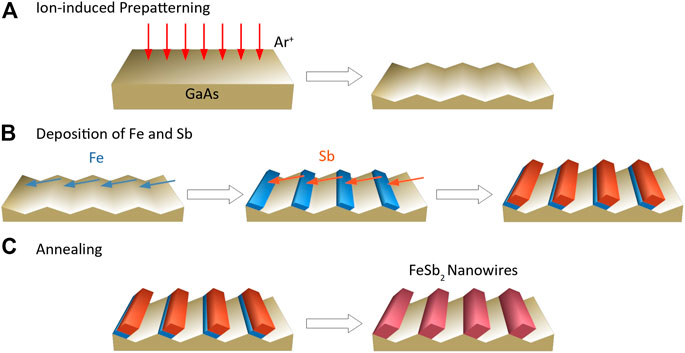
FIGURE 1. Schematic of the bottom-up fabrication of FeSb2 nanowires on crystalline GaAs substrates. (A) Ion-induced pre-patterning of the GaAs substrate with Ar+ ions. (B) Successive deposition of Fe and Sb on the pre-patterned substrate. (C) Annealing of the deposited nanostructures.
For the substrates, we used single-crystalline GaAs(001) (CrysTec GmbH, Germany). The samples had a size of 10 × 10 mm2 and the
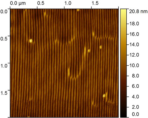
FIGURE 2. Topography image of a GaAs(001) surface after 1 keV Ar+ ion irradiation at normal incidence with an ion fluence of 3 × 1019 cm−2 at 400 °C recorded by atomic force microscopy.
The fabrication of the FeSb2 nanowires was accomplished by successive physical vapor deposition (PVD) of Fe and Sb in the same vacuum system without exposing the nanostructured GaAs(001) surface to air. For the Fe deposition, we used an electron beam evaporator (UHV Evaporator EFM 3, Focus GmbH, Germany). The mounted Fe bar (MaTeck GmbH, Germany) had a diameter of 2 mm and a purity of 99.99%. For the Sb deposition, we used a low-temperature effusion cell (NTEZ 40-10-22-KS-2107228, Dr. Eberl MBE-Komponenten GmbH, Germany) and Sb granules (MaTeck GmbH, Germany) with 0.5–1.0 mm diameter and a purity of 99.9999%. To fabricate nanowires, it was necessary to perform deposition under a glancing angle of >74°, since the rippled structure of GaAs(001) had an inclination angle of 16° [5]. Therefore, we deposited Fe and Sb at an angle of 80°. The deposition was done successively with a desired height ratio of deposited Fe-layer to deposited Sb-layer of about 1:5 to achieve the correct stoichimetric ratio for FeSb2. This was estimated by the density of Fe and Sb. The deposition rates were 0.14 nm min−1 for Fe and 0.35 nm min−1 for Sb, respectively. These rates were determined on a flat GaAs surface with removed native oxide layer at normal incidence. After deposition, the samples were annealed in vacuum at 250 °C in the same vacuum system.
To characterize the microstructure of the as-prepared and annealed samples, transmission electron microscopy (TEM) was performed. To this end, classical TEM cross-sections of the samples glued together in face-to-face geometry using G2 epoxy glue (Gatan Inc., United States) were prepared by sawing (Wire Saw WS 22, IBS GmbH, Germany), grinding (MetaServ 250, Bühler, Germany), polishing (Minimet 1,000, Bühler, Germany), dimpling (Dimple Grinder 656, Gatan Inc., United States), and final Ar ion milling (Precision Ion Polishing System PIPS 691, Gatan Inc., United States). Bright-field and high-resolution TEM (HR-TEM) imaging were done using an image-Cs-corrected Titan 80–300 microscope (FEI, United States) operated at an accelerating voltage of 300 kV. High-angle annular dark-field scanning transmission electron microscopy (HAADF-STEM) imaging and spectrum imaging analysis based on energy-dispersive X-ray spectroscopy (EDXS) were performed at 200 kV using a Talos F200X microscope equipped with a Super-X EDXS detector system (FEI, United States). Prior to (S)TEM analysis, each specimen mounted in a high-visibility low-background holder was placed for 8 s into a Model 1,020 Plasma Cleaner (Fischione Inc., United States) to remove potential contaminations. Determination of the formed crystalline Fe-Sb phases was done by fast Fourier transform (FFT) analysis of selected cross-sectional nanowire regions. In particular, potential zone axis diffractograms were calculated from the recorded HR-TEM images and compared with simulated diffraction patterns of hexagonal FeSb [37] and orthorhombic FeSb2 [38] using the JEMS software package. Additionally, quantitative element analysis was performed on sum spectra obtained from selected nanowire cross-sections. In particular, spectrum quantification including bremsstrahlung background correction based on the physical TEM model, series fit peak deconvolution, and application of tabulated theoretical Cliff-Lorimer factors was done for the elements Fe (K line series) and Sb (L line series) using the ESPRIT software version 1.9 (Bruker, United States).
We prepared four samples with different deposition order and heat treatment. The parameters for the sample preparation are summarized in Table 1. To prepare the samples, we first ion-irradiated the GaAs(001) substrate to create a template for the nanowires. The ion-induced nanostructure of the GaAs(001) surface is characterized by almost perfectly parallel-aligned ripples besides some defects in the surface structure like bifurcation points, where two ripples are merged together. Such defects can be seen in Figure 2 in the upper right area, where a row of bifurcation points is visible. These bifurcation points are caused by the dynamics of the self-organized surface structuring process. Since we used a broad ion beam, the entire surface of the sample was irradiated and the growth of small ripples starts simultaneously in a random distribution. During this process, bifurcation points are created between phase-shifted ripple regions, which can move along the ripples while irradiating. With increasing irradiation time, oppositely orientated bifurcation points annihilate each other until isolated defects are formed. Thus, the bifurcation point density decreases with increasing irradiation time [39]. After preparing the template for the nanowires, we successively deposited Fe and Sb under glancing incidence. Samples 1 and 2 were not annealed after deposition to investigate the as-deposited structure of the nanowires. To prepare FeSb2 nanowires, in the samples 3 and 4, we annealed them after the successive deposition of Fe and Sb. As described in Table 1, we changed the deposition order of Fe and Sb for the samples with and without annealing. For each sample, a representative cross-sectional overview bright-field TEM image, a HR-TEM image of one individual ripple with a deposited nanowire, and the corresponding EDXS-based element distribution are shown in Figures 3–6.
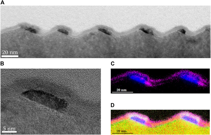
FIGURE 3. Sample 1 cross-sectional overview bright-field TEM image in (A) and HR-TEM image of an individual nanowire in (B) with corresponding EDXS-based element distributions of Fe and Sb in (C), and of Fe, Sb, Ga, As, and O in (D). Fe was deposited before Sb, and the sample was not annealed. EDXS coloring: Fe - blue, Sb - magenta, Ga - red, As - green, oxygen - white (yellow due to additive color mixing of green and red).
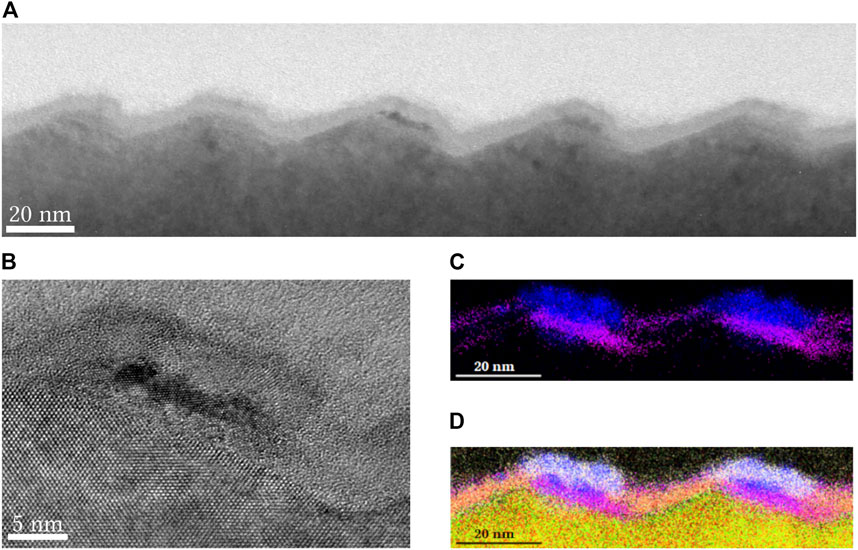
FIGURE 4. Sample 2 cross-sectional overview bright-field TEM image in (A) and HR-TEM image of an individual nanowire in (B) with corresponding EDXS-based element distributions of Fe and Sb in (C), and of Fe, Sb, Ga, As, and O in (D). Sb was deposited before Fe, and the sample was not annealed. EDXS coloring: Fe - blue, Sb - magenta, Ga - red, As - green, oxygen - white (yellow due to additive color mixing of green and red).
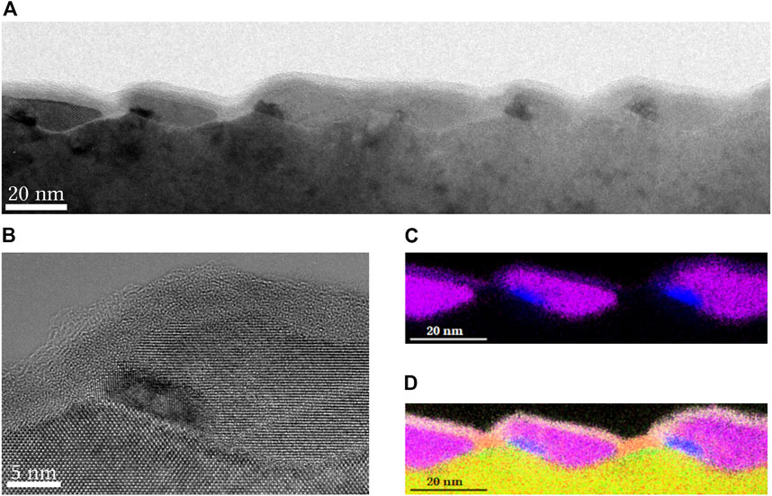
FIGURE 5. Sample 3 cross-sectional overview bright-field TEM image in (A) and HR-TEM image of an individual nanowire in (B) with corresponding EDXS-based element distributions of Fe and Sb in (C), and of Fe, Sb, Ga, As, and O in (D). Fe was deposited before Sb, and the sample was annealed for 75 min at 250 °C. EDXS coloring: Fe - blue, Sb - magenta, Ga - red, As - green, oxygen - white (yellow due to additive color mixing of green and red).
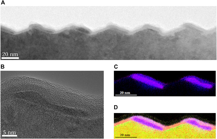
FIGURE 6. Sample 4 cross-sectional overview bright-field TEM image in (A) and HR-TEM image of an individual nanowire in (B) with corresponding EDXS-based element distributions of Fe and Sb in (C), and of Fe, Sb, Ga, As, and O in (D). Sb was deposited before Fe, and the sample was annealed for 30 min at 250 °C. EDXS coloring: Fe - blue, Sb - magenta, Ga - red, As - green, oxygen - white (yellow due to additive color mixing of green and red).
The cross-sectional overview bright-field TEM images in Figure 3A, Figure 4A, Figure 5A, Figure 6A confirm the rippled GaAs surface. Furthermore, they indicate the presence of nanowire-like structures, which—except for sample 3—are quite uniform and mainly located on the right ripple side (see Supplementary Figure S1, Supplementary Material for an SEM image of sample 2, confirming the uniformity of the nanowires over a length of more than 1 μm). All samples seem to be covered by a cap layer. On top of it, there is the glue used during TEM specimen preparation, which, for samples 3 and 4, ruptured from the cap layer during TEM analysis. The HR-TEM images (Figure 3B; Figure 4B; Figure 5B; Figure 6B) confirm the single-crystalline nature of the GaAs substrate. The internal structure of the nanowires will be discussed for each sample below. According to the EDXS-based element distributions in Figure 3D, Figure 4D, Figure 5D, Figure 6D, all samples are covered by an oxide cap layer. While the nanowire determines the type of the oxide on the right ripple sides, an amorphous Ga oxide forms on the left ripple sides.
For the as-deposited samples 1 and 2, the different setup of the Fe and Sb layers is clearly observable. In sample 2, as expected, Sb is detected underneath the Fe layer which gets oxidized on top. In addition, small amounts of Sb are present on top of the Ga oxide on the opposite ripple side and Fe is located within the Sb part. Since Fe is not soluble in Sb [40], the detected Fe is more likely caused by a non-continuous Sb layer. In sample 1, however, Fe is detected near the top ridges of the ripples and Sb near the ripple troughs. Instead of the expected double-layer formation, like in sample 2, Fe and Sb are located beside each other. On the other hand, Sb is detected again on top of the Ga oxide as well as on the Fe oxide and also in small amounts between Fe and its oxide. The enclosed Sb between Fe and its oxide suggests a non-continuous Sb layer, while the detected Sb on top of the oxides in samples 1 and 2 points to a high diffusivity, especially if Sb is not covered by Fe.
Despite the high diffusivity of Sb, the annealed samples 3 and 4 formed individual nanowires with a mostly parallelogram-shaped cross-section. The height (respective to the deposited surface) is determined by the deposition time and is (10.0 ± 1.7) nm for sample 3 and (6.6 ± 0.8) nm for sample 4, respectively. The height is not completely homogeneous, which leads to occasionally connected nanowires for sample 3. While the nanowires of sample 4 show complete Fe-Sb phase formation, there is a remaining Fe-rich core for each of the nanowires in sample 3. For both samples, a Fe-Sb oxide forms on top of the nanowires.
In samples 1 and 3, the Fe component and the GaAs substrate have the same orientation. In particular, corresponding FFTs from the cross-sectional HR-TEM images can be described with the body-centered cubic structure of Fe and the zincblende structure of GaAs in [
To identify the crystalline Fe-Sb phases in the samples 3 and 4, quantitative EDXS analysis was performed on 10 different nanowire cross-sections for each sample. Additionally, FFT analysis was carried out on appropriate cross-sectional nanowire regions, as described in the experimental section. In particular, we found one region for sample 3 and three regions for sample 4 suitable for FFT analysis (see Supplementary Figures S2–S5, Supplementary Material). Regarding sample 3, EDXS analysis shows a Fe content of (33.9 ± 2.0) at.–% and a Sb content of (66.1 ± 2.0) at.–%. This agrees well with the result of the FFT analysis, where the diffractogram could be described with the orthorhombic FeSb2 structure in [001] zone axis orientation (Fig. S2). Thus, both EDXS and FFT analysis reveal FeSb2 formation for sample 3. Regarding sample 4, EDXS analysis of 9 nanowires shows a Fe content of (32.5 ± 3.1) at.–% and a Sb content of (67.5 ± 3.1) at.–%. The two corresponding diffractograms match with the orthorhombic FeSb2 structure in [211] (Supplementary Figure S3) and [120] zone axis orientation (Supplementary Figure S4), respectively. The third diffractogram can be described with the hexagonal FeSb structure in [100] zone axis orientation (Supplementary Figure S5), and EDXS analysis of the same area shows a Fe:Sb ratio of 43:57. Thus, in the case of sample 4, EDXS and FFT analysis reveal predominant FeSb2 formation besides the presence of small amounts of FeSb.
Although a stoichiometric ratio for FeSb2 was aspired for samples 3 and 4, the deposited ratio was wrong. In sample 3, the Fe phase is present in every observed nanowire, while in sample 4, the Fe-richer FeSb phase was detected besides FeSb2. This indicates a total Fe:Sb ratio shifted to a higher Fe content, probably caused by a lower deposition rate of Sb on a structured surface under glancing incidence than on a flat surface under normal incidence, as it was used to determine the deposition rate in advance. As described earlier, Sb seems to form a non-continuous layer on GaAs(001) and Fe. During the determination of the deposition rate, Sb island formation was observed. This points to a quite weak Sb-surface interaction, leading to low adhesion of Sb and a lower deposition rate on a structured surface under glancing incidence. However, it seems to be more favorable to prepare FeSb2 nanowires on GaAs(001) by annealing Sb on top of epitaxially grown Fe. With this deposition order, excess Fe remains present, indicating that it is energetically more favorable for the system than forming the undesired FeSb phase like in sample 4. However, FeSb2 nanowires with a Sb deficiency could be favorable for thermoelectric applications. Sanchela et al. [42] and Li et al. [43] reported the improvement of the thermoelectric properties for polycrystalline FeSb2 with a Sb deficiency. This is based on the reduction of the phononic thermal conductivity as well as the increase of the Seebeck coefficient. Additionally, Li et al. [43] described a two orders of magnitude higher electrical conductivity for thin films of FeSb2-x (x = 0, 0.1, 0.2, 0.3). In view of these results, it would be interesting to advance our approach for nanostructuring FeSb2 with an improved control of the deposited Fe:Sb ratio.
We successfully prepared FeSb2 nanowires in a bottom-up process. To this end, we used low-energy ion irradiation of GaAs(001) at normal incidence to create a template with an ordered parallel-aligned rippled surface structure. The nanowire preparation was done with PVD of Fe and Sb under glancing angle and annealing in vacuum. This enables to prepare nanowires with a variable cross-sectional size up to 22 × 22 nm2, which is the maximum size for separated nanowires on GaAs(001) with an ion-induced nanopatterned surface, before interconnection of the individual nanowires occurs. We showed that it is possible to prepare single-phase nanowires as well as nanowires with a layered structure, which are almost perfectly parallel-aligned, like the template. This is particularly advantageous for electrical contacting. The HR-TEM images we used for the characterization showed that Fe growth is epitaxial on nanostructured GaAs(001). These epitaxially grown Fe nanowires could be an approach for the further development of single-crystalline FeSb2 nanowires with an optimized deposition and annealing regime. In the case of FeSb2, single-crystalline nanowires as well as polycrysatlline nanowires with a defined Sb deficiency could lead to a possible improvement of thermoelctric devices for cryogenic applications.
This bottum-up fabrication method for nanowires is, due to the used PVD process, quite independent of the material, and therefore, it is suitable for several application possibilities, e.g., thermoelectric, catalytic, magnetic, optical, or biological devices. For an even wider range of possible applications, it is necessary to find a solution to remove the nanowires from the substrate. In summary, the presented bottom-up nanofabrication offers a simple and robust method to create parallel-ordered nanowires.
The raw data supporting the conclusion of this article will be made available by the authors, without undue reservation.
TW prepared the samples and conducted the AFM measurements. RH performed the TEM-based investigations. DE conceptualized the study, designed it with TW, and supervised the experimental work. SF lead the project. All authors contributed to data interpretation and jointly wrote the manuscript.
We carried out all experimental parts of this research at the Ion Beam Center of the Helmholtz-Zentrum Dresden-Rossendorf e.V.—a member of the Helmholtz Association. The authors thank Romy Aniol for TEM specimen preparation. Furthermore, the funding of TEM Talos by the German Federal Ministry of Education and Research (BMBF; grant No. 03SF0451) in the framework of HEMCP is acknowledged.
The authors declare that the research was conducted in the absence of any commercial or financial relationships that could be construed as a potential conflict of interest.
All claims expressed in this article are solely those of the authors and do not necessarily represent those of their affiliated organizations, or those of the publisher, the editors and the reviewers. Any product that may be evaluated in this article, or claim that may be made by its manufacturer, is not guaranteed or endorsed by the publisher.
The Supplementary Material for this article can be found online at: https://www.frontiersin.org/articles/10.3389/fphy.2023.1149608/full#supplementary-material
1. Cuerno R, Kim JS. A perspective on nanoscale pattern formation at surfaces by ion-beam irradiation. J Appl Phys (2020) 128:180902. doi:10.1063/5.0021308
2. Facsko S, Dekorsy T, Koerdt C, Trappe C, Kurz H, Vogt A, et al. formation of ordered nanoscale semiconductor dots by ion sputtering. Science (1999) 285:1551–3. Cited References Count:16. doi:10.1126/science.285.5433.1551
3. Ou X, Keller A, Helm M, Fassbender J, Facsko S. Reverse epitaxy of ge: Ordered and faceted surface patterns. Phys Rev Lett (2013) 111:016101. doi:10.1103/physrevlett.111.016101
4. Chowdhury D, Ghose D, Mollick SA. Homoepitaxy of germanium by hyperthermal ion irradiation. Vaccum (2014) 107:23–7. doi:10.1016/j.vacuum.2014.03.022
5. Ou X, Heinig KH, Hübner R, Grenzer J, Wang X, Helm M, et al. Faceted nanostructure arrays with extreme regularity by self-assembly of vacancies. Nanoscale (2015) 7:18928–35. doi:10.1039/c5nr04297f
6. Ziberi B, Cornejo M, Frost F, Rauschenbach B. Highly ordered nanopatterns on Ge and Si surfaces by ion beam sputtering. J Phys Condensed Matter (2009) 21:224003. Cited References Count:63. doi:10.1088/0953-8984/21/22/224003
7. Sigmund P. Theory of sputtering. i. sputtering yield of amorphous and polycrystalline targets. Phys Rev (1969) 184:768–416. doi:10.1103/physrev.187.768
8. Bradley RM, Harper JME. Theory of ripple topography induced by ion bombardment. J Vacuum Sci Tech A: Vacuum, Surf Films (1988) 6:2390–5. doi:10.1116/1.575561
9. Carter G, Vishnyakov V. Roughening and ripple instabilities on ion-bombarded si. Phys Rev B (1996) 54:17647–53. doi:10.1103/physrevb.54.17647
10. Mullins WW. Flattening of a nearly plane solid surface due to capillarity. J Appl Phys (1959) 30:77–83. doi:10.1063/1.1734979
11. Umbach CC, Headrick RL, Chang KC. Spontaneous nanoscale corrugation of ion-eroded SiO2: The role of ion-irradiation-enhanced viscous flow. Phys Rev Lett (2001) 87:246104. 500TD Times Cited: 32 Cited Reference Count: 25 246104. doi:10.1103/PhysRevLett.87.246104
12. Shipman PD, Bradley RM. Theory of nanoscale pattern formation induced by normal-incidence ion bombardment of binary compounds. Phys Rev B (2011) 84:085420. doi:10.1103/physrevb.84.085420
13. Valbusa U, Boragno C, de Mongeot FB. Nanostructuring surfaces by ion sputtering. J Phys Condensed Matter (2002) 14:8153–75. doi:10.1088/0953-8984/14/35/301
14. Schwoebel RL, Shipsey EJ. Step motion on crystal surfaces. J Appl Phys (1966) 37:3682–6. doi:10.1063/1.1707904
15. Chan WL, Chason E. Making waves: Kinetic processes controlling surface evolution during low energy ion sputtering. J Appl Phys (2007) 101:121301. doi:10.1063/1.2749198
16. Chowdhury D, Ghose D. Highly-ordered ripple structure induced by normal incidence sputtering on monocrystalline GaAs (001): Ion energy and flux dependence. Vaccum (2016) 129:122–5. doi:10.1016/j.vacuum.2016.04.019
17. Toma A, Chiappe D, Massabò D, Boragno C, de Mongeot FB. Self-organized metal nanowire arrays with tunable optical anisotropy. Appl Phys Lett (2008) 93:163104. doi:10.1063/1.3002319
18. Ranjan M, Facsko S. Anisotropic surface enhanced Raman scattering in nanoparticle and nanowire arrays. Nanotechnology (2012) 23:485307. doi:10.1088/0957-4484/23/48/485307
19. Ranjan M, Facsko S, Fritzsche M, Mukherjee S. Plasmon resonance tuning in ag nanoparticles arrays grown on ripple patterned templates. Microelectronic Eng (2013) 102:44–7. doi:10.1016/j.mee.2012.02.018
20. D’Andrea C, Fazio B, Gucciardi PG, Giordano MC, Martella C, Chiappe D, et al. SERS enhancement and field confinement in nanosensors based on self-organized gold nanowires produced by ion-beam sputtering. The J Phys Chem C (2014) 118:8571–80. doi:10.1021/jp5007236
21. Gkogkou D, Schreiber B, Shaykhutdinov T, Ly HK, Kuhlmann U, Gernert U, et al. Polarization- and wavelength-dependent surface-enhanced Raman spectroscopy using optically anisotropic rippled substrates for sensing. ACS Sensors (2016) 1:318–23. doi:10.1021/acssensors.5b00176
22. Li Y, Cui F, Ross MB, Kim D, Sun Y, Yang P. Structure-sensitive co2 electroreduction to hydrocarbons on ultrathin 5-fold twinned copper nanowires. Nano Lett (2017) 17:1312–7. doi:10.1021/acs.nanolett.6b05287
23. Kim D, Xie C, Becknell N, Yu Y, Karamad M, Chan K, et al. Electrochemical activation of CO2 through atomic ordering transformations of AuCu nanoparticles. J Am Chem Soc (2017) 139:8329–36. doi:10.1021/jacs.7b03516
24. Schreier M, Héroguel F, Steier L, Ahmad S, Luterbacher JS, Mayer MT, et al. Solar conversion of CO2 to CO using earth-abundant electrocatalysts prepared by atomic layer modification of CuO. Nat Energ (2017) 2:17087. doi:10.1038/nenergy.2017.87
25. Teschome B, Facsko S, Gothelf KV, Keller A. Alignment of gold nanoparticle-decorated DNA origami nanotubes: Substrate prepatterning versus molecular combing. Langmuir (2015) 31:12823–9. doi:10.1021/acs.langmuir.5b02569
26. Wittenbrink I, Hausmann A, Schickle K, Lauria I, Davtalab R, Foss M, et al. Low-aspect ratio nanopatterns on bioinert alumina influence the response and morphology of osteoblast-like cells. Biomaterials (2015) 62:58–65. doi:10.1016/j.biomaterials.2015.05.026
27. Liedke MO, Körner M, Lenz K, Grossmann F, Facsko S, Fassbender J. Magnetic anisotropy engineering: Single-crystalline fe films on ion eroded ripple surfaces. Appl Phys Lett (2012) 100:242405. doi:10.1063/1.4729151
28. Körner M, Röder F, Lenz K, Fritzsche M, Lindner J, Lichte H, et al. Quantitative imaging of the magnetic configuration of modulated nanostructures by electron holography. Small (2014) 10:5161. doi:10.1002/smll.201400377
29. Arranz MA, Colino JM, Palomares FJ. On the limits of uniaxial magnetic anisotropy tuning by a ripple surface pattern. J Appl Phys (2014) 115:183906. doi:10.1063/1.4876232
30. Ki S, Dho J. Strong uniaxial magnetic anisotropy in triangular wave-like ferromagnetic NiFe thin films. Appl Phys Lett (2015) 106:212404. doi:10.1063/1.4921784
31. Chen ZG, Han G, Yang L, Cheng L, Zou J. Nanostructured thermoelectric materials: Current research and future challenge. Prog Nat Sci Mater Int (2012) 22:535–49. doi:10.1016/j.pnsc.2012.11.011
32. Vineis CJ, Shakouri A, Majumdar A, Kanatzidis MG. Nanostructured thermoelectrics: Big efficiency gains from small features. Adv Mater (2010) 22:3970–80. doi:10.1002/adma.201000839
33. Boukai AI, Bunimovich Y, Tahir-Kheli J, Yu JK, Goddard WA, Heath JR. Silicon nanowires as efficient thermoelectric materials. Nature (2008) 451:168–71. doi:10.1038/nature06458
34. Bentien A, Johnsen S, Madsen GKH, Iversen BB, Steglich F. Colossal seebeck coefficient in strongly correlated semiconductor FeSb 2. Europhysics Lett (Epl) (2007) 80:17008. doi:10.1209/0295-5075/80/17008
35. Jie Q, Hu R, Bozin E, Llobet A, Zaliznyak I, Petrovic C, et al. Electronic thermoelectric power factor and metal-insulator transition in fesb2. Phys Rev B (2012) 86:115121. doi:10.1103/physrevb.86.115121
36. Williams JR, Johnson M, Johnson DC. Composition dependence of the nucleation energy of iron antimonides from modulated elemental reactants. J Am Chem Soc (2001) 123:1645–9. doi:10.1021/ja003791d
37. Kjekshus A, Walseth KP, Rasmussen SE, Heinegård D, Balaban AT, Craig JC. On the properties of the cr(1+x)sb, fe(1+x)sb, co(1+x)sb, ni(1+x)sb, pd(1+x)sb, and pt(1+x)sb phases. Acta Chemica Scand (1969) 23:2621–30. doi:10.3891/acta.chem.scand.23-2621
38. Holseth H, Kjekshus A, Harnung SE, Lundström H, Borch G, Craig JC. Compounds with the marcasite type crystal structure. IV. the crystal structure of FeSb2. Acta Chemica Scand (1969) 23:3043–50. doi:10.3891/acta.chem.scand.23-3043
39. Malsch G. Untersuchung der topologischen Defekte in Oberflächenstrukturen auf GaAs und InAs unter niedrig energetischem Ionenbeschuss. Dresden: Technische Universität Dresden (2017). Master thesis.
40. Richter KW, Ipser H. Reinvestigation of the binary fe-sb phase diagram. J Alloys Comp (1997) 247:247–9. doi:10.1016/s0925-8388(96)02597-2
41. Waldrop JR, Grant RW. Interface chemistry of metal-GaAs Schottky-barrier contacts. Appl Phys Lett (1979) 34:630–2. doi:10.1063/1.90642
42. Sanchela AV, Thakur AD, Tomy C. Enhancement in thermoelectric properties of FeSb2 by sb site deficiency. J Materiomics (2015) 1:205–12. doi:10.1016/j.jmat.2015.04.005
Keywords: bottom-up nanofabrication, ion-induced nanopatterning, physical vapor deposition, transmission electron microscopy, energy-dispersive X-ray spectroscopy
Citation: Weinert T, Hübner R, Facsko S and Erb DJ (2023) Bottom-up fabrication of FeSb2 nanowires on crystalline GaAs substrates with ion-induced pre-patterning. Front. Phys. 11:1149608. doi: 10.3389/fphy.2023.1149608
Received: 22 January 2023; Accepted: 10 March 2023;
Published: 30 March 2023.
Edited by:
Indra Sulania, Inter-University Accelerator Centre (IUAC), IndiaReviewed by:
Mukesh Ranjan, Institute for Plasma Research (IPR), IndiaCopyright © 2023 Weinert, Hübner, Facsko and Erb. This is an open-access article distributed under the terms of the Creative Commons Attribution License (CC BY). The use, distribution or reproduction in other forums is permitted, provided the original author(s) and the copyright owner(s) are credited and that the original publication in this journal is cited, in accordance with accepted academic practice. No use, distribution or reproduction is permitted which does not comply with these terms.
*Correspondence: Tom Weinert, dC53ZWluZXJ0QGh6ZHIuZGU=; Denise J. Erb, ZC5lcmJAaHpkci5kZQ==
†ORCID: Tom Weinert, orcid.org/0009-0003-8687-6096; René Hübner, orcid.org/0000-0002-5200-6928; Stefan Facsko, orcid.org/0000-0003-3698-3793; Denise J. Erb, orcid.org/0000-0002-5831-7284
Disclaimer: All claims expressed in this article are solely those of the authors and do not necessarily represent those of their affiliated organizations, or those of the publisher, the editors and the reviewers. Any product that may be evaluated in this article or claim that may be made by its manufacturer is not guaranteed or endorsed by the publisher.
Research integrity at Frontiers

Learn more about the work of our research integrity team to safeguard the quality of each article we publish.